Note: Descriptions are shown in the official language in which they were submitted.
CA 02365956 2001-10-03
WO 00/77529 PCT/US00/14189
-1-
Description
METHOD AND APPARATUS FOR TESTING A
VIDEO DISPLAY CHIP
TECHNICAL FIELD OF THE INVENTION
The present relates generally to video display
chips and more specifically to a method and apparatus for
testing video display chips.
BACKGROUND ART
A video chip typically comprises a matrix of
pixels consisting of a storage capacitor and a pass
transistor. Data stored in the various capacitors
collectively comprise a video image. The stored image is
"read" out by shining a light on the chip and visually
scanning the image.
This mode of outputting the stored contents
poses a problem in the manufacture of such chips.
Testing a video chip is not possible until the chip is
packaged so that it is functional as an imaging device.
This permits a test image to be loaded into the device
and then visually inspected for defects. Defective
devices can then be identified, removed from the lot and
discarded. Thus, a defect is not detected until the chip
is fully packaged. This is a costly process because the
manufacturing cost has already been invested in producing
the packaged part, which has now been determined to be
defective.
It is therefore desirable to have the
capability of screening out defective video chips prior
to their being packaged in a final form. What is needed
is a scheme for providing a suite of tests to the chip to
CA 02365956 2001-10-03
WO 00/77529 PCT/US00/14189
-2-
fully verify the operability of the device before final
packaging of the device.
SUMMARY OF THE INVENTION
A method for testing a video chip comprising a
plurality of signal lines arranged in matrix form in
accordance with the invention includes applying a voltage
potential to one end of the signal lines, driving the
gates of a series-connected chain of transistor with the
other end of the signal lines, applying a voltage at one
end of the transistor chain, and detecting a potential at
the other end of the transistor chain. The method
further includes loading an input bit pattern at one end
of the signal lines and detecting the pattern which forms
at the other end of the signal lines. By comparing the
input pattern against the detected pattern various
defects in the signal lines can be detected.
A video chip in accordance with the present
invention includes a matrix of video storage elements, a
column selector for loading a row of a video image into a
selected row in the matrix, a row selector for selecting
a row in the matrix. The video chip further includes a
column test register disposed opposite the column
selector so that the column lines are connected
therebetween. Similarly, a row test register is disposed
opposite the row selector so that the row lines are
connected therebetween.
The column selector includes register for
receiving an input test pattern and means for driving the
test pattern onto the column lines. The column test
registers receive a pattern at the other end of the
column lines whereby defects in the column lines can be
determined by comparing the input test pattern against
the pattern stored in the column test register.
CA 02365956 2001-10-03
WO 00/77529 PCT/US00/14189
-3-
The row selector includes registers for
receiving an input test pattern and means for driving the
test pattern onto the row lines. The row test registers
receive a pattern at the other end of the row lines
whereby defects in the row lines can be determined by
comparing the input test pattern against the pattern
stored in the row test registers.
BRIEF DESCRIPTION OF THE DRAWINGS
Fig. 1 is a block diagram of a video chip of
the present invention.
Fig. 2 is a block diagram of the test registers
shown in Fig. 1.
Fig. 3 is a block diagram of the shift
registers shown in Fig. 2.
Figs. 4 and 5 are block diagrams of the column
and row registers shown in Fig. 1.
Fig. 6 shows a typical storage cell.
Fig. 7 shows a detection of a fault in
accordance with the present invention.
BEST MODE FOR CARRYING OUT THE INVENTION
Referring to Fig. l, a video chip 100 comprises
a matrix 10 of storage elements 12 arranged in row and
column order. A typical storage element is shown in Fig.
6, comprising a pass transistor 14 coupled to deliver a
charge to a capacitor 16. Each storage element 12 has an
associated column (data) line 114 and a row (word) select
line 112. Typically, a scan line of a video signal is
received by a column register 104 which then drives the
signal onto each of column lines 114. A primary row
select register 102 drives a control signal onto a
selected one of row lines 112 so that the video signal
carried by column lines 114 is transferred through pass
CA 02365956 2001-10-03
WO 00/77529 PCT/L1S00/14189
-4-
transistors 14 into capacitors 16 comprising the storage
elements of the selected row.
The column register 104 of the present
invention includes a test input 136 for receiving a
column test signal YTST. Column test signal YTST
comprises a bit pattern that is serially shifted in via
clock signal CCLK. Similarly, row register 102 includes
a test input 138 for receiving a row test signal XTST
(also a pattern of bits), which clocked in via clock
signal RCLK.
Turn for a moment to the block diagrams for
column and row registers 104 and 102 shown in Figs. 4 and
5. As shown in Fig. 4, column register 104 comprises a
register bank 402, the outputs of which constitute column
lines 114. Signal CCLK serially clocks data from a mux
404 into register bank 402. Mux 404 is coupled to
receive as input video scan line VIDEO and test data
YTST. Depending on column enable signal CEN, either the
video signal or the test signal will be serially shifted
into register bank 402. As shown in Fig. 4, asserting
column enable signal CEN puts column register 104 in
video output mode, while test mode is entered by
de-asserting CEN.
Fig. 5 shows that row register 102 consists of
a decoder 502 and a register bank 504, each of whose
outputs are OR'd together by OR gates 506. The outputs
of the OR gates constitute row lines 112. Decoder 502
includes an active-hi enable input while register bank
504 includes an active-to enable input. Thus, either the
decoder or the register bank is enabled at any one time
by row enable signal REN so that row lines 112 carry only
one set of signals. Video mode is selected by asserting
enable signal REN, while test mode is selected by
de-asserting REN. In video mode, decoder 502 receives
CA 02365956 2001-10-03
WO 00/77529 PCT/US00/14189
_5_
select signal RSEL to energize the row line associated
with the current scan line. In test mode, as will be
explained below, the row lines 112 each is driven with a
logic one or a logic zero. This is achieved by serially
clocking in a test pattern into register bank 504 from
XTST under the control of clock signal RCLK and
de-asserting enable signal REN.
Returning to Fig. 1, it can be seen that the
far ends of each of column lines 114 and row lines 112
respectively feed into a column test register 124 and a
row test register 122. Both test registers 122 and 124
have an input for receiving a voltage potential Vdd.
Column test register 124 receives a clock signal T CCLK
and a register clear signal T CLR. Likewise, row test
register 122 receives a clock signal T RCLK and the same
register clear signal T CLR. It is noted that the row
test register can be cleared by its own register clear
signal. However, it is typical that both test registers
will be cleared at the same time and so a single clear
signal is sufficient.
Each test register 122 and 124 is provided with
two outputs. A continuity output RC CONT from each test
register is coupled to a single test node 130. Column
test register 124 includes a serial output 134, while row
test register 122 is provided with serial output 132.
Although the preferred embodiment shows that the
continuity outputs of the test registers are tied to node
130, this is not necessary. The single node 130 is
preferred since it is contemplated that row and column
continuity tests (explained below) will be performed
separately. Also, a single output node is preferred
since it minimizes the pin-count of the device.
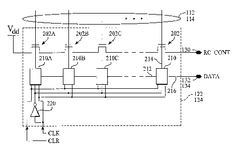
Referring to Fig. 2, it can be seen that each
of the test registers 122 and 124 includes a
CA 02365956 2001-10-03
WO 00/77529 PCT/US00/14189
-6-
series-connected chain of transistors 202. A first end
of the transistor chain is coupled to Vdd and a second
end is coupled to node 130. Fig. 2 shows the use of
N-channel transistors, although P-channel devices can be
used. The source terminal of a previous transistor 202B
is coupled to the drain terminal of a subsequent
transistor 202C. The gate of each transistor 202 is
coupled to the far end of a column (data) line 114 in the
case of column test register 124 or a row (word) line 112
in the case of row test register 122.
It is also clear from Fig. 2 that the column
and word lines 114 and 112 in each test register 124 and
122 additionally feed into a bank of series-connected
flip-flop circuits 210. These flip-flop circuits
together constitute the register portion of test
registers 122 and 124. Each flip-flop circuit 210 is
provided with two inputs: a first input 214 for receiving
either a column or a row line 124 and 122; and a second
input 212 being coupled to the output 216 of a previous
flip-flop circuit. Each flip-flop circuit also receives
a clocking signal CLK; T CCLK in the case of column test
register 124 and T RCLK for row test register 122. In
addition, a complement of the clock signal is provided
via inverter 220. Finally, an input is provided for a
CLR signal to reset each flip-flop circuit. The output
216 of the last flip-flop circuit in the register bank is
coupled to node 132 in the case of row test register 122
and to node 134 in the case of column test register 124.
Referring now to Fig. 3, the flip-flop circuits
of the present invention each consists of a pair of NOR
gates 302 and 304. The NOR gates are cross-coupled, the
output of gate 302 being coupled to an inverted input of
gate 304 and the output of gate 304 being coupled to a
non-inverted input of gate 302 through pass transistor
CA 02365956 2001-10-03
WO 00/77529 PCT/US00/14189
326. An inverted input of gate 302 receives first input
214, which will either be a column line or a row line,
while its non-inverted input is coupled to second input
212 through pass transistor 322. A non-inverted input of
gate 304 receives the CLR signal to reset the flip-flop
circuit.
The output of gate 302 is coupled to a latch
circuit through pass transistor 324. The latch circuit
is comprised of inverters 312 and 314 coupled in a
feedback configuration through pass transistor 328. The
output of inverter 312 is coupled to output 216 of the
flip-flop circuit. Pass transistors 326 and 324 are
turned on by positive edges of the clock signal, while
pass transistor 322 and 328 are turned on by negative
going edges of the clock.
The discussion will now turn to the method of
testing the column and row lines in accordance with the
invention. Consider a continuity test of column lines
114. With reference to Fig. 1, a pattern of bits is
serially shifted into column register 104 via test input
136, one bit for each column line. In the case of a
continuity test, the bit pattern is simply all ones.
Next, the pattern is output onto column lines 114, thus
transferring the bit pattern into column test register
124. The potential at node 130 is monitored. Referring
to Fig. 2, it can be seen that initially the transistors
202 comprising the transistor chain in column test
register 124 are all turned off. The potential at node
130 therefore is said to be tri-stated, i.e. in a high
impedance state, floating, disconnected. When the input
pattern is driven onto the column lines, some or all of
the transistors will be turned on. In the case where all
of column lines 114 are intact, each transistor 202 will
be turned on. Consequently, the potential appearing at
CA 02365956 2001-10-03
WO 00/77529 PCT/US00/14189
_g-
node 130 will be (Vdd - Vth), where Vth is the threshold
voltage of the transistors and assuming that a logic one
is Vdd. On the other hand, where one or more of column
lines 114 is an open; then the corresponding transistor
202 will be non-conductive, and thus node 130 will remain
tri-stated. Thus, by monitoring node 130 for a change
from its initial tri-state condition to a non-tri-stated
condition, an indication is given that there is
continuity among all of the column lines.
A continuity test of row lines 112 is
accomplished in the same way as for column line 114.
First, a pattern of ones is serially shifted into row
register 102 via test input 138. Each of the bits in the
pattern are simultaneously driven onto the row lines 112,
thus transferring the pattern into row test register 122.
If all the row lines are intact, then node 130 will
change from a tri-sated condition to having a potential
of (Vdd - Vth), again assuming logic ones are at a
potential of Vdd. If any of the row lines has an open,
node 130 will remain in its initial tri-stated condition.
Although a continuity test is adequate for
determining whether any column or row line is
compromised, the test provides no information as to which
of the lines are open. Moreover, the test does not
detect the presence of shorted lines. A more
comprehensive test is provided by the register portion
(flip-flop circuits 210) of test registers 122 and 124.
First, the column (row) register 104 (102) is
serially loaded via test input 136 (138) with a bit
pattern of alternating ones and zeroes. Next, the
pattern is driven onto the column (row) lines and clocked
into the flip-flop circuits of the column (row) test
register 124 (122). The bit pattern stored in the
flip-flop circuits is then clocked out onto node 134
CA 02365956 2001-10-03
WO 00/77529 PCT/US00/14189
-9-
(132) one bit at a time. Faults in the column (row)
lines can be determined by comparing the pattern that is
read out of the registers against the input bit pattern.
For example, since the input pattern is an alternation of
ones and zeroes, a pair of shorted lines would produce
two consecutive ones in the readout pattern.
More specific fault identification is possible
by using an appropriate test pattern of bits. For
example, each line (column or row) can be individually
tested for an open or a short condition. Beginning with
the line in the most significant bit position, the test
pattern would consist of a one in the MSB position and
zeroes in the other bit positions. The pattern is driven
on the lines and received at the far end in the register
bank of the test register (122 or 124). The pattern is
shifted out of the register bank and examined. If the
MSB of the readout pattern is zero, then an open exists.
If the readout pattern contains a one in other bit
positions, then shorts exist. The next line is tested by
shifting the bit to the next position in the test pattern
and repeating the above steps.
As can be seen the above examples, various
fault conditions can be deduced by applying the
appropriate bit pattern, clocking it into the test
register, and reading out the pattern from the test
register. As a final example, consider Fig. 7 which
shows a set of column or row lines 124 or 122. One of
the lines exhibits an open 702, while an adjacent line
shows a short 704 to the open line, the short being
downstream of the open. Applying input test pattern IN1
to the column or row register 104 or 102 will produce
output pattern OUT1 at the corresponding test register.
Notice that the open prevents the logic one in test
pattern IN1 from appearing in output pattern OUT1. Next,
CA 02365956 2001-10-03
WO 00/77529 PCT/~JS00/14189
-10-
a second test pattern IN2 is applied. The output is
output pattern OUT2. As can be seen, the output shows
two ones and by comparing OUT1 with OUT2, a conclusion
can be made as to the nature of the fault. This example
therefore shows that the application of multiple input
patterns and the analysis of the output patterns may be
required in order to detect certain faults.