Note: Descriptions are shown in the official language in which they were submitted.
CA 02366039 2001-12-20 FPO1-0204-00
TITLE OF THE INVENTION
Optical Amplifier, Optical Communication System
Including the Same, and Optical Fiber Module Included in
the Same
BACKGROUND OF THE INVENTION
Field of the Invention
The present invention relates to an optical amplifier
applicable to wavelength division multiplexing (WDM)
transmission systems, an optical communication system
including the optical amplifier, and an optical fiber module
constituting a part of the optical amplifier.
Related Background Art
In WDM transmission systems including optical
amplifiers as optical communication systems OADM (Optical
Add/Drop Multiplexes) and OXC (Optical Cross Connect) have
recently been incorporated as structures for separating a
part of multiplexed signals by signal channel units or sending
out a predetermined wavelength of signals or multiplexed
signals to transmission lines by signal channel units in
order to improve the reliability and operating efficiency
of each system as a whole. In such a WDM system, attention
is paid to transitional output signal power fluctuations
in optical amplifiers occurring due to changes in the number
of channels of inputted signals. Therefore, it is required
for optical amplifiers to be controlled such that the output
signal power (output signal level) per channel becomes
1
CA 02366039 2001-12-20 FPO1-0204-~~
constant even if the input power changes.
As means for suppressing the transitional output signal
powerfluctuations caused byinputsignalpowerfluctuations
occurring due to changes in the number of signal channels,
high-speed automatic gain control (AGC) has been proposed.
Here, the response speed of AGC is required to become
faster as the speed at which the number of signal channels
changes is faster, and as the number of the added or dropped
signal increases.
As a technique for speeding up AGC, Seo Yeon Park, et
al., "Dynamic Gain and Output Power Control in a
Gain-Flattened Erbium-Doped Fiber Amplifier," IEEE
PHOTONICS TECHNOLOGY LETTERS, Vol. 10, No. 6, JUNE 1998,
for example, proposes feed-forward controlby detecting only
the power of input signal (input signal level) , and a pumping
light power corresponding to the power of input signal is
calculated by use of a linear expression, so as to maintain
a constant gain. This AGC technique can achieve higher speed
more easily as compared with conventional feedback control,
whereby a response time of 650 ns is realized in actually
developed control circuits.
SUMMARY OF THE INVENTION
The inventor has studied the prior art and, as a result,
has found a problem as follows . Namely, even if feed-forward
control is carried out in a conventional optical amplifier
by detecting power fluctuations in input signals, the control
2
CA 02366039 2001-12-20 FPOl-0204-00
starting time will be delayed due to a delay in a control
circuit, whereby overshoot may occur by the amount of delay
in the control circuit.
If the response time of the control circuit controlling
a pumping light source is substantially zero, the power of
pumping light outputted from the pumping light source can
be regulated at substantially the same time when a power
fluctuation in input signals is detected in the vicinity
of an input end of an optical amplifier (the fluctuation
is detected before amplification), whereby transient power
fluctuations in output signals will hardly occur. However,
actual control circuits have a response time to a certain
extent. Therefore, even if a power fluctuation in input
signals is detected in the vicinity of an input end of an
optical amplifier (at the point of time indicated by arrow
A in Fig. 1), a transient power fluctuation (dynamic gain
fluctuation PD) in output signals will occur in an optical
amplifier for the duration of response time t1 of the control
circuit after the actual power fluctuation in input signals
is generated as shown in Fig. 1 (see A.K. Srivastava, et
al., "EDFA Transient Response to Channel Loss in WDM
Transmission System," IEEE PHOTONICS TECHNOLOGY LETTERS,
Vol. 9, No. 3, MARCH 1997) . Also, Y. Sun et al., "Fast power
transients in WDM optical networks with cascaded EDFAs,"
ELECTRONIC LETTERS, 13th Feb. 1997, Vol. 3, No. 4 indicate
that transient gain fluctuations accumulate in a system in
3
CA 02366039 2001-12-20 FPO1-0204-~0
which optical amplifiers (EDFAs) are connected in a
multistage fashion.
However, the change delay time of the pumping light
power evaluated in the above-mentioned Srivastava reference
with respect to the power fluctuation in input signals is
7 us or more, whereby it is unknown whether the transient
power fluctuation in output signals can fully be suppressed
or not if the delay time further approaches zero. Also, it
does not mention any difference in response of the optical
amplifier depending on the wavelength of pumping light.
In order to overcome the above-mentioned problem, it
is an object of the present invention to provide an optical
amplifier comprising a structure which can effectively
suppress transient output signal power fluctuations (gain
fluctuations) occurring due to delays in control, an optical
fiber module included in the same, and an optical
communication system comprising a structure for effectively
restraining the power fluctuations from accumulating.
The optical amplifier according to the present
invention is an optical device, employed in a WDM transmission
system for transmitting a plurality of channels of signals
included in a predetermined signal wavelength band, for
amplifying the signals propagating through an optical
transmission line included in the WDM transmission system.
In order to overcome the above-mentioned problem, the
optical amplifier according to the present invention
4
CA 02366039 2001-12-20 FPO1-0204-00
comprises, at least, a branching device, a light-receiving
device, an amplification optical device (amplification
optical fiber) , a pumping light source, a delay medium, and
a control system. The branching device taps part of light
including the signals propagating through the optical
transmission line. The light-receiving device detects a
power fluctuation (level fluctuation) of the part of light
tapped by the branching device. The amplification optical
fiber is an optical fiber doped with a rare-earth element
or the like for amplifying the signals. The pumping light
source launches pumping light of a predetermined wavelength.
into the amplification optical fiber. The delay medium is
an optical device, arranged between the branching device
and the amplification optical fiber, for delaying the light
reaching the input end of the amplification optical fiber
from the branching device. The control system monitors, by
way of the light-receiving device, the power of the part
of light tapped by the branching device, and controls the
pumping light source.
Transient power fluctuations in output signals can
fully be suppressed if the pumping light power can
intentionallybe changed at the same time when the fluctuation
in input signal level occurring in the vicinity of the input
end of the optical amplifier is detected (the amount of change
in pumping light power being adjusted according to the amount
of fluctuation in input signal power). However, it is
5
CA 02366039 2001-12-20 FPO1-0204-00
unrealistic for the response time from the detection of
fluctuation to the power control of pumping light to become
zero. Therefore, the present invention utilizes the delay
medium, so as to delay the signal input to the amplification
optical fiber, thus making it possible to detect the input
signal power before amplification.
Preferably, in the optical amplifier according to the
present invention, the delay medium has an insertion loss
of 3 dB or less. This is because of the fact that it can
effectively restrain transient or dynamic power fluctuations
from occurring due to changes in the number of signal channels
while suppressing an excess degradation of noise figure.
Specifically, it is preferred that the signal delay
time given by the delay medium be at least 1 us but not longer
than 50 us. Preferably, the delay medium includes a
single-mode optical fiber having a length of at least 0.2
km but not longer than 10 km. Since the transmission loss
of a single-mode optical fiber is usually about 0.2 dB/km,
it can minimize the degradation of noise figure in the optical
amplifier, and can delay input signals to the amplification
optical fiber by a time within the range of 1 us to 50 us.
As the optical fiber employed in the delay medium, a pure
silica core fiber having a low loss and a low bending loss
is preferable for allowing the optical amplifier to realize
a smaller size.
In the case where the delay medium is longer, the delay
6
CA 02366039 2001-12-20 FPO1-0204-00
medium preferably includes a dispersion-shifted optical
fiber in order to restrain the dispersion of the delay medium
itself from increasing. The delay medium may also include
a dispersion-compensating optical fiber arranged between
the single-mode optical fiber and the amplification optical
fiber. This is because of the fact that, when a high-speed
operation is required in L band ( 1565 nm to 1620 nm) in the
optical amplifier, it will be preferable if the dispersion
of the amplification optical fiber is compensated for in
order to improve the dispersion tolerance of the optical
amplifier.
The inventor has also found that the response
characteristic of the optical amplifier depends on the
pumping light wavelength. In the case of an optical amplifier
employing 0. 98 um as its pumping light wavelength, the signal
delay time given by the delay medium must be longer than
the response time of the control system from when the signal
power fluctuation is detected until when the control of the
pumping light source is started. This is because of the fact
that transient power fluctuations of an output signal cannot
fully be suppressed in the optical amplifier pumped with
the pumping light having a wavelength of 0.98 ~.un even when
the pumping light power is changed at substantially the same
time when the power of an input signal fluctuates. In the
case of the optical amplifier employing 0. 98 um as its pumping
light wavelength, the signal delay time given by the delay
7
CA 02366039 2001-12-20 FPO1-0204-00
medium is preferably adjusted such that, in terms of the
transient fluctuation of the gain in the optical amplifier
caused by a power fluctuation in the input signal with respect
to a target gain, the gain yields an overshoot amount and
an undershoot amount which are substantially identical to
each other.
In the case of an optical amplifier employing 1.98 pm
as its pumping light wavelength, it is preferred that the
signal delay time given by the delay medium be substantially
identical to the response time of the control system from
when the signal power fluctuation is detected until when
the control of the pumping light source is started. This
is because of the fact that transient power fluctuations
of the output signal can fully be suppressed in this case
unlike the above-mentioned case where the pumping light
wavelength is 0.98 ~.im.
Preferably, the signal delay time given by the delay
medium is adjusted so as to become longer than the sampling
time of the control system for monitoring the light tapped
by.the branching device. This aims at making it possible
to adjust the pumping light power in conformity to power
fluctuations in input signals.
The control system carries out AGC by ut i1 i zing a 1 inear
expression Pp -a~P~ +b (where a and b are constants) which
provides a relationship between the power PIN of the part
of light tapped by the branching device and the power Pp of
8
CA 02366039 2001-12-20 FPO1-0204-00
the pumping light outputted from the pumping light source.
This aims at enabling high-speed control by use of
feed-forward control. However, even when transient power
fluctuations in the output signal are suppressed during the
control time t2 as shown in Fig. l, there is a possibility
of a static gain fluctuation PQ occurring if AGC is carried
out in a state where the average value (time average) of
saturation power of output signals varies between before
and after the fluctuation.
Therefore, it is preferred that the optical amplifier
according to the present invention further comprise a
spectrum analyzer for monitoring a signal distribution within
a signal wavelength band at the output end of the amplification
optical fiber. Here, the control system detects the signal
distribution within the signal wavelength band at the output
end of the amplification optical fiber, and updates the
constants a and b in the above-mentioned linear expression
utilized for AGC.
For effectively suppressing the static gain
fluctuation PQ, the control system may update the constants
a and b in the above-mentioned linear expression utilized
for AGC by using an amplification factor (P~,T/PIN) given by
the ratio between the amplified optical power Pour at the
output end of the amplification optical fiber and the power
PIN of the part of light tapped by the branching device.
Preferably, the optical amplifier according to the
9
CA 02366039 2001-12-20 FPO1-0204-00
present invention further comprises a branching device for
tapping part of amplified light transmitted through the
amplification optical fiber, and a light-receiving device
for detecting a power of the light tapped by the branching
device. In this case,the controlsystem monitors respective
powers of parts of light tapped by the two branching devices
disposed upstream and downstream the amplification optical
fiber by way of their correspondinglight-receiving devices,
and controls the pumping light source so as to adjust the
pumping light power according to results of detection
obtained by these light-receiving devices.
The optical communication system according to the
presentinvention includesa plurality of optical amplifiers
at least one of which has a structure identical to that of
the optical amplifier comprising the structure mentioned
above. Preferably, this optical communication system
comprises a structure for enabling at least one of a branching
function of tapping part of multiplexed signals propagating
through a transmission line by a signal channel unit, and
an inserting function of sending out a predetermined
wavelength of signals or multiplexed signals to a
transmission line by a signal channel unit, e.g., OADM or
OXC.
The optical amplifier according to the present
invention preferably includes an optical fiber module having
respective terminals to be connected to the light-receiving
CA 02366039 2001-12-20 FPO1-0204-~~
device, pumping light source, and optical transmission line
so as to reduce the insertion loss of the optical amplifier.
The optical fiber module comprises a single-mode optical
fiber to be fusion-spliced to the optical transmission line,
a delay fiber acting as the delay medium to be fusion-spliced
to the single-mode optical fiber, an amplification optical
fiber to be fusion-spliced to the delay fiber, a first fiber
coupler for tapping part of light including a signal having
reached the optical amplifier before being fed to the delay
fiber, and a second fiber coupler for supplying the pumping
light from at least one of the input and output ends of the
amplification optical fiber.
Specifically, the single-mode optical fiber has a first
end to be fusion-spliced to the output end of the optical
transmission line through which a plurality of channels of
signals included in a predetermined signal wavelength band
propagate, and a second end opposing the first ends and
constitutes a part of the optical transmission line. The
delay fiber has a first end fusion-spliced to the second
end of single-mode optical fiber, and a second end opposing
the first end. The amplification optical fiber has a first
end fusion-spliced to the second end of delay fiber, and
a second end opposing the first end. The first fiber coupler
is arranged near a fused part between the second end of
single-mode optical fiber and the first end of delay fiber.
Preferably, the second fiber coupler is arranged near a fused
11
CA 02366039 2001-12-20 FPO1-0204-~~
part between the second end of delay fiber and the first
end of amplification optical fiber, or near the second end
of amplification optical fiber.
The present invention will be more fully understood
from the detailed description given hereinbelow and the
accompanying drawings, which are given by way of illustration
only and are not to be considered as limiting the present
invention.
Further scope of applicability of the present invention
will become apparent from the detailed description given
hereinafter. However, it should be understood that the
detailed description and specific examples, while indicating
preferred embodiments of the invention, are given by way
of illustration only, since various changesandmodifications
within the spirit and scope of the invention will be apparent
to those skilled in the art from this detailed description.
BRIEF DESCRIPTION OF THE DRAWINGS
Fig. 1 is a graph for explaining a problem of AGC in
a conventional optical amplifier:
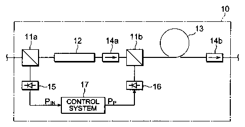
Fig. 2 is a diagram showing the configuration of a first
embodiment of the optical amplifier according to the present
invention
Fig. 3 is a diagram showing a specific configuration
of the optical fiber module according to the present
invention
Fig. 4 is a diagram showing the configuration of a second
12
CA 02366039 2001-12-20 FPO1-0204-00
embodiment of the optical amplifier according to the present
invention;
Fig. 5 is a diagram showing the configuration of a third
embodiment of the optical amplifier according to the present
invention;
Fig. 6 is a diagram showing the configuration of a fourth
embodiment of the optical amplifier according to the present
invention;
Fig. 7 is a diagram showing the configuration of a fifth
embodiment of the optical amplifier according to the present
invention;
Fig. 8 is a diagram showing the structure of an
experimental system for evaluating the amount of transient
power fluctuation in output signals caused by the delay in
pumping light power change with respect to changes in the
number of signal channels;
Fig. 9A is a diagram showing the structure of an optical
amplifier utilizing pumping light having a wavelength of
0.98 um as an optical amplifier (EDFA) employed in the
experimental system shown in Fig. 8, whereas Fig. 9B is a
diagram showing the structure of an optical amplifier
utilizing pumping light having a wavelength of 1.48 um;
Fig. 10A is a graph showing the time response of total
input power in the experimental system shown in Fig. 8, whereas
Fig. lOB is a graph showing the time response of pumping
light power;
13
CA 02366039 2001-12-20 FPO1-0204-00
Fig. 11A is a graph showing the transient response
characteristic with respect to a residual signal having a
wavelength of 1551.7 nm concerning the optical amplifier
having a pumping light wavelength of 0.98 um shown in Fig.
9A, whereas Fig. 11B is a graph showing the transient response
characteristic with respect to a residual signal having a
wavelength of 1551.7 nm concerning the optical amplifier
having a pumping light wavelength of 1.48 um shown in Fig.
9B~
Fig. 121 is a graph showing the dependence of transient
response characteristic upon delay time concerning the
optical amplifier having a pumping light wavelength of 0.98
~.un shown in Fig. 9A with respect to each of residual signals
having a wavelength ranging from 1531.7 nm to 1561.4 nm,
whereas Fig. 12B is a graph showing the dependence of transient
response characteristic upon delay time concerning the
optical amplifier having a pumping light wavelength of 1 .48
dun shown in Fig. 9B with respect to each of residual signals
having a wavelength ranging from 1531.7 nm to 1561.4 nm~
and
Fig. 13A is a graph showing the transient response
characteristic with respect to a residual signal having a
wavelength of 1551. 7 nm in the case where a single-mode optical
fiber having a length of 400 nm is not employed as the delay
medium in the optical amplifier shown in Fig. 5, whereas
Fig. 13B is a graph showing the transient response
14
CA 02366039 2001-12-20 FPO1-0204-00
characteristic with respect to a residual signal having a
wavelength of 1551 . 7 nm in the case where a single-mode optical
fiber having a length of 400 nm is employed as the delay
medium in the optical amplifier shown in Fig. 5.
DESCRIPTION OF THE PREFERRED EMBODIMENTS
In the following, embodiments of the optical amplifier
according to the present invention and the optical fiber
module included therein will be explained with reference
to Figs. 2 to 8 and 9A to 13B. In the explanation of drawings,
constituents identical to each other will be referred to
with numerals identical to each other without repeating their
overlapping descriptions. The proportions of dimensions in
the drawings do not always match those explained.
Fig. 2 is a diagram showing the configuration of a first
embodiment of the optical fiber amplifier according to the
present invention. In Fig. 2, the optical amplifier 10
according to the first embodiment comprises, successively
in the advancing direction of signal light, a branching device
11a, a delay medium 12, an optical isolator 14a, amultiplexer
11b, an amplification optical fiber 13, and an optical
isolator 14b, which constitute a part of an optical
transmission line. The branching device lla taps part of
light including a plurality of channels of signals having
reached there from an optical transmission line. The delay
medium 12 functions such that signals transmitted through
the branching device lla delay reaching the input end of
CA 02366039 2001-12-20 FPO1-0204-00
the amplification optical fiber 13. The multiplexer llb
combines pumping light and the signal transmitted through
the delay medium 12, and launches thus combined light into
the amplification optical fiber 13 from the input end side
thereof.
The optical amplifier 10 further comprises a
light-receiving device 15 (PD) for monitoring the power of
the part of light tapped by the branching device l la, a pumping
light source 16 (LD) , and a control system 17 which controls
the pumping light source 16 in conformity to power
fluctuations of the tapped part of light tin a feed-forward
control fashion) while monitoring the power of tapped part
of light by way of the light-receiving device 15.
In general, the gain coefficient ys in an optical
amplifier having an amplification optical fiber doped with
erbium or the like is approximately represented by the
following expression (1):
Ys ~ ~ (1)
1 + PP - 1's
PP P~
where
g is the unsaturated gain;
PPth is the threshold power of pumping light
Pe is the pumping light power;
PS is the signal power; and
Psat is the saturation power.
16
CA 02366039 2001-12-20 FPO1-0204-00
According to the above-mentioned expression (1), for
making the gain coefficient yS constant, i.e., for making
the gain of optical amplifier constant, it will be sufficient
i f ( Ppth ~ PS ) / ( PPth , Psat ) i s made cons tant . I f the power o f
input signal is determined, then the pumping light power
necessary for AGC is calculated by the above-mentioned
expression (1). Therefore, utilizing this expression (1)
enables AGC based on feed-forward control (regulating the
pumping light power while monitoring only the input signal
power) . Here, the pumping light power Pe necessary for the
above-mentioned AGC can be represented by the following
linear expression (2):
Pp=a~PQ"+b (2)
where
Pp is the pumping light power
PIN is the input signal powers and
a and b are constants.
Feed-forward control can realize higher-speed AGC as
compared with feedback control in which input and output
are detected. However, if the signal power is detected at
the input end of the optical amplifier, and the pumping light
power is controlled according to the result of detection,
then the power of input signals will fluctuate by the response
time of the control system, whereby a transient power
fluctuation may occur in output signals.
A.K. Srivastava, "EDFA Transient Response to Channel
17
CA 02366039 2001-12-20 FPO1-0204-00
Loss in WDM Transmission System," IEEE PHOTONICS TECHNOLOGY
LETTERS, Vol. 9, No. 3, MARCH 1997 reports transient output
signal power fluctuations caused by delays in regulation
of pumping light power with respect to power fluctuations
in input signals. From this report, it can be seen that the
transient power fluctuations in output signals can be
suppressed more as delays in regulation of pumping light
power with respect to power fluctuations in input signals
are smaller. Ideally, the transient power fluctuations in
output signals can substantially be suppressed to zero if
the pumping light power can be changed by an appropriate
amount at the same time when a power fluctuation is generated
in input signals. Though the response time in the control
system may be made sufficiently short in order to address
the above-mentioned problem, there is a limit to shortening
the response time of the control system.
Therefore, the optical amplifier according to the
present invention is provided with a structure for delaying
signals to a certain extent (at least by the response time
of the control system) during the period of time from when
a change in power of input signals is detected until when
a fluctuation in signal power occurs at the input end of
the amplification optical fiber. This structure can make
the power fluctuation timing of input signals at the input
end of amplification optical fiber and the fluctuation timing
of pumping light power coincide with each other, whereby
18
CA 02366039 2001-12-20 FP01-0204-00
the transient power fluctuations in output signals can be
suppressed effectively. Also, since the input signals are
delayed by an appropriate amount, the response speed required
for the control system is alleviated, which makes it easier
to design the control system.
Operations of the optical amplifier 10 according to
the first embodiment will now be explained with reference
to Fig. 2. In the optical amplifier 10, part of light
including a plurality of channels of signals propagated
through an optical transmission line is tapped by the
branching device 11a, and power fluctuations of thus tapped
part of light are detected by the light-receiving device
15. On the other hand, the remaining part of light
transmitted through the branching device 11a passes through
the delay medium 12, optical isolator 14a, and multiplexer
llb in succession, so as to reach the amplification optical
fiber 13. While the light transmitted through the branching
device lla is propagating through the delay medium 12, the
control system 17 detects the power fluctuation of input
signals by way of the light-receiving device 15, and controls
the pumping light source 16 so as to change the pumping light
power.
At the input end of amplification optical fiber 13,
due to the foregoing configuration, the input signals and
pumping light attain a state where their respective power
fluctuations aresubstantiallysynchronized with each other.
19
CA 02366039 2001-12-20 FPOl-0204-00
As a result, signals amplified by the optimized gain are
outputted from the amplification optical fiber 13, and thus
amplified signals are sent out to an optical transmission
line by way of the optical isolator 14b.
For improving the noise figure of the optical amplifier
10, it is necessary that at least the loss at the input end
of amplification optical fiber 13 be made as low as possible.
Therefore, it is preferred that the insertion loss of the
delay medium 12 inserted into the input end side of the
amplification optical fiber 13 be as small as possible. In
this regard, a single-mode optical fiber having an insertion
loss of 3 dB or less is suitable, and can yield a delay of
about 5 us per km.
In the case where an optical fiber having a large
chromatic dispersion is employed as an optical fiber acting
as the delay medium 12 (hereinafter referred to as delay
fiber), a separate dispersion-compensating optical fiber
is necessary. Preferably, the delay fiber has a chromatic
dispersion which is as small as possible, since it eliminates
the need for inserting a separate optical fiber which
compensates for the dispersion. In the case where the delay
fiber is longer, the delay fiber preferably includes a
dispersion-shifted optical fiber in order to restrain the
dispersion of the delay fiber itself from increasing. The
delay fiber may include a dispersion-compensating optical
fiber disposed between the single-mode optical fiber and
CA 02366039 2001-12-20 FPO1-0204-00
the amplification optical fiber. This is because of the fact
that, when a high-speed operation is required in L band (1565
nm to 1620 nm) in the optical amplifier, it is preferred
that the dispersion of the amplification optical fiber 13
be compensated for in order to improve the dispersion
tolerance of the optical amplifier 10.
In general, a WDM transmission system having a
transmission capacity per signal channel of 10 Gbit/s can
permit a cumulative dispersion up to (1000 ps/nm. From this
fact, a dispersion of ~200 ps/nm or less caused by the delay
fiber is considered to be a permissible range in a WDM
transmission system in which five stages of repeaters are
inserted. It is needless to say that the cumulative
dispersion should be further lowered as the transmission
capacity per signal channel increases from now on.
As mentioned above, the optical amplifier according
to the present invention preferably includes an optical fiber
module having respective terminals to be connected to the
above-mentioned light-receiving device, pumping light
source, and optical transmission line in order to reduce
the insertion loss of the optical amplifier as shown in Fig.
3. The optical fiber module shown in Fig. 3 comprises a
single-mode optical fiber 100 to be fusion-spliced to the
optical transmission line, a delay fiber 110 (corresponding
to the delay medium l2 in Fig. 2) to be fusion-spliced to
the single-mode optical fiber 100, an amplification optical
21
CA 02366039 2001-12-20 FPO1-0204-00
fiber 120 (corresponding to the amplification optical fiber
13 in Fig. 2) to be fusion-spliced to the delay fiber 110,
a first fiber coupler 150 (corresponding to the branching
device lla in Fig. 2) for tapping part of light including
signals having reached the optical amplifier before being
fed into the delay fiber 110, and a second fiber coupler
160 (corresponding to the multiplexer llb in Fig. 2) for
supplying pumping light from at least one of the input and
output ends of the amplification optical fiber 120. Thus,
the input ends of the fiber couplers 150, 160 to which the
light-receiving device and pumping light source are to be
connected are open in the optical fiber module shown in Fig.
3, whereby users can select the light-receiving device and
pumping light source in conformity to the design
specification of the whole WDM transmission system.
Specifically, the single-mode optical fiber 100 in Fig.
3 has a first end to be fusion-spliced to the output end
of the optical transmission line through which a plurality
of channels of signals included in a predetermined signal
wavelength band propagate, and a second end opposing the
first end, thereby constituting a part of the optical
transmission line. The delay fiber 110 has a first end
fusion-spliced to the second end of single-mode optical fiber
100, and a second end opposing the first end. The
amplification optical fiber 120 has a first end
fusion-spliced to the second end of delay fiber 110, and
22
CA 02366039 2001-12-20 FPO1-0204-0~
a second end opposing the first end. The first fiber coupler
150 is disposed near the fused part between the second end
of single-mode optical fiber 100 and the first end of delay
fiber 110. The second fiber coupler 160 is disposed near
the fused part between the second end of delay fiber 110
and the first end of amplification optical fiber 120. For
suppressing the deterioration of noise figure to the minimum,
as mentioned above, the delay fiber 110 preferably includes
an optical fiber having an insertion loss of 3 dB or less .
In the case where the delay fiber 110 is longer, it preferably
includes a dispersion-shifted optical fiber. For
compensating for the dispersion of amplification optical
fiber 120, the delay fiber 110 may include a
dispersion-compensating optical fiber.
Ideally, since it is necessary to regulate (change)
the pumping light power at the same time when the power of
input signals fluctuates, the delay time applied by the delay
medium 12 to signals is required to be substantially on a
par with the response time of the control system 17 ( including
an arithmetic processing circuit)for controlling the pumping
light source 16. In particular, it is necessary that the
sampling time for detecting the input signal power be set
sufficiently shorter than the signal delay time given by
the delay medium 12. If the sampling time is longer than
the signal delay time, then the timing for detecting the
power fluctuation itself delays, whereby the delay applied
23
CA 02366039 2001-12-20 FP,O1-0204-0~
to signals becomes meaningless . The sampling time is also
determined by the speed at which the subject input signal
power fluctuates.
In the case where the pumping light source 16 changes
substantially stepwise, it will be sufficient if the signal
delay time given by the delay medium 12 and the response
time of the control system 17 (the period of time from when
the fluctuation is detected until when the pumping light
source 16 is controlled) are made identical to each other.
In practice, however, waveforms are somewhat broad.
Therefore, if the signal delay time is set slightly longer
than the response time of control system 17, then the transient
power fluctuations in output signals can effectively be
suppressed.
In the feed-forward control (AGC) based on the
above-mentioned expressions ( 1 ) and ( 2 ) , AGC can be carried
out by use of the above-mentioned expression (2) when the
average value of saturation power of multiplexed signals
is the same between before and after the power of input signals
fluctuates. However, the saturation power is dependent on
wavelength, so that the average value of saturation power
is not always constant between before and after the
fluctuation when the power of input signals fluctuates due
to changes in the number of signal channels (see Fig. 1).
In the case where the average value of saturation power varies,
a static gain fluctuation PQ will occur if AGC is carried
24
CA 02366039 2001-12-20 FPO1-0204-00
out with the constants a ( gradient ) and b ( intercept ) being
fixed.
For suppressing such a static gain fluctuation PQ, it
is preferred that the position of signal wavelength within
a signal wavelength band be monitored, and that the constants
a, b in the above-mentioned expression (2) be regulated
according to thus detected signal distribution.
Fig. 4 is a diagram showing the configuration of a second
embodiment of the optical amplifier according to the present
invention accomplished based on the consideration mentioned
above.
As shown in Fig. 4, the,optical amplifier 20 according
to the second embodiment has the same configuration as that
of the first embodiment in that it comprises a branching
device 21a, a delay medium 22, an optical isolator 24a, a
multiplexer 21b, an amplification optical fiber 23, an
optical isolator 24b, a light-receiving device 25, a pumping
light source 26, and a control system 27. However, in order
to suppress the above-mentioned static gain fluctuation,
the optical amplifier 20 according to the second embodiment
further comprises a branching device 21c for tapping part
of light including output signals from the amplification
optical fiber 23, and a spectrum analyzer 28 for monitoring
the signal distribution within the signal wavelength band
concerning the part of light tapped by the branching device
21c.
CA 02366039 2001-12-20 FPO1-0204-00
' The control system 27 carries out AGC by utilizing the
above-mentioned linear expression of PP ~ a ~P~, +b (where a
and b are constants) defining the relationship between the
power PIN of the part of light tapped by the branching device
21a and the power PP of pumping light outputted from the pumping
light source . It aims at enabling higher-speed control based
on feed-forward control. However, even when the
above-mentioned transient output signal level fluctuations
are suppressed during the control time t2, there is a
possibility of the static gain variation PQ occurring if AGC
is carried out in a state where the average value ( time average )
of saturation power of output signals varies between before
and after a fluctuation as shown in Fig. 1. Therefore, in
the optical amplifier 20 according to the second embodiment,
the control system 27 detects the signal distribution within
the signal wavelength band at the output end of amplification
optical fiber 23 by way of the spectrum analyzer 28, so as
to update the constants a and b in the above-mentioned linear
expression (2) utilized for AGC, thereby effectively
suppressing the static gain fluctuation PQ.
Fig. 5 is a diagram showing the configuration of a third
embodiment of the optical amplifier according to the present
invention, which is characterized in that it comprises a
configuration for lowering the static gain fluctuation PQ
(see Fig. 1) as in the second embodiment.
Namely, as shown in Fig. 5, the optical amplifier 30
26
CA 02366039 2001-12-20 FP01-0204-~~
according to the third embodiment has the same configuration
as that of the first and second embodiments in that it comprises
a branching device 31a, a delay medium 32, an optical isolator
34a, a multiplexes 31b, an amplification optical fiber 33,
an optical isolator 34b, a light-receiving device 35, a
pumping light source 36, and a control system 37. However,
in order to suppress the above-mentioned static gain
fluctuation, the optical amplifier 30 according to the third
embodiment further comprises a branching device 31c for
tapping part of light including output signals from the
amplification opticalfiber33, and alight-receiving device
38 for detecting the power of the part of light tapped by
the branching device 31c.
The control system 37 updates the constants a and b
in the above-mentioned linear expression (2) utilized for
AGC by using an amplification factor (PouT/PIN) given by the
ratio of the amplified optical power Pour at the output end
of the amplification optical fiber 33 to the power PIN of
the part of light tapped by the branching device 31a.
Further, the optical amplifier according to the present
invention can be modified in various manners . For example,
there are many optical amplifiers each comprising a plurality
of stages of amplifying sections. In such a configuration,
if a delay medium is inserted immediately upstream the
amplifying section at each stage, then the transmission loss
within the optical amplifier increases, thereby
27
CA 02366039 2001-12-20 FPOl-0204-00
deteriorating noise characteristics, which is unfavorable.
Therefore, the optical amplifier according to a fourth
embodiment comprises a structure in which a delay medium
is inserted immediately upstream only the amplifying section
at the first stage, the power of signals before reaching
the delay medium is detected, and the pumping light power
is regulated for the amplifying section at each stage
according to the result of detection.
Fig. 6 is a diagram showing the configuration of the
fourth embodiment of the optical amplifier according to the
present invention. In Fig. 6, the optical amplifier 40
according to the fourth embodiment comprises, successively
in the advancing direction of signals propagated through
the optical transmission line, a branching device 41 for
tapping part of light including the signals, a delay medium
42, a plurality of stages of amplifying sections 43a to 43c
(each comprising an amplification optical fiber and a pumping
light source), a light-receiving device 44, and a control
system 45 for feed-forward control (AGC) of each of the
plurality of stages of amplifying sections 43a to 43c.
Since the optical amplifier 40 according to the fourth
embodiment is configured such that the branching device 41
is provided upstream the plurality of stages of amplifying
sections 43a to 43c, whereas part of light (including the
signals) tapped by the branching device 41 is monitored,
power fluctuations in input signals can be detected more
28
CA 02366039 2001-12-20 FPO1-0204-00
rapidly than in a configuration in which power fluctuations
in input signals are detected immediately upstream each
amplifying section, thus enablingAGCwhich favorably follows
the power fluctuations in input signals . Also, in the optical
amplifier 40 according to the fourth embodiment, the delay
medium 42 is disposed between the branching device 41 and
the amplifying section 43a at the first stage in order for
the respective timings for detecting the power fluctuation
in input signals at the plurality of stages of amplifying
sections 43a to 43c and regulating the pumping light power
(outputting control signals PPl to PP3 from the control system
45 to respective pumping light sources included in the
individual amplifying sections 43a to 43c) to apparently
coincide with each other.
The optical amplifier 40 according to the fourth
embodiment comprising the plurality of stages of amplifying
sections 43a to 43c downstream the delay medium 42 as such
is suitable for WDM transmission systems in which OADM
(OpticalAdd/Drop Multiplexer),OXC(OpticalCross Connect),
and the like are inserted.
In a WDM transmission system incorporated with OADM
or OXC, there are often cases where the power fluctuation
in input signals to the optical amplifier abruptly changes
due to changes in the number of signal channels. In such
a case, the applied optical amplifier is required to rapidly
control the gain so as to keep it constant. The optical
29
CA 02366039 2001-12-20 FPO1-0204-00
amplifier 40 according to the fourth embodiment can detect
the power fluctuation in input signals to each of the plurality
of amplifying sections 43a to 43c before amplification, and
can effectively suppress transient output signal power
fluctuations.
The optical amplifier according to the present
invention may further comprise a configuration in which
signals to be fed into the delay medium are amplified
beforehand.
Fig. 7 is a diagram showing the configuration of a fifth
embodiment of the optical amplifier according to the present
invention.
Basically as in the first embodiment, the optical
amplifier 50 according to the fifth embodiment comprises,
successively in the advancing direction of signals, a
branching device 51a, a delay medium 52, an optical isolator
54a, a multiplexes 51b, an amplification optical fiber 53,
and an optical isolator 54b, which constitute a part of an
optical transmission line. It further comprises a
light-receiving device 55 for monitoring power fluctuations
of the part of light tapped by the branching device 51a,
and a pumping light source 56 for supplying pumping light
to the amplification optical fiber by way of the multiplexes
51b~ and is configured such that a control system 57 detects
power fluctuations in input signals by way of the
light-receiving device 55 and controls (in AGG fashion) the
CA 02366039 2001-12-20 FPO1-0204-00
pumping light source 56.
In particular, the optical amplifier 50 according to
the fifth embodiment is characterized in that an amplifying
section 58 (including an amplification optical fiber 58a)
for amplifying input signals before detection is disposed
upstream the branching device 51a. Disposed between the
amplifying section 58 and the branching device 51a is an
optical device 59 comprising one of a variable attenuator
and a band-pass filter. Hence, in the optical amplifier 50
according to the fifth embodiment, a part of the optical
transmission line is constituted by at least the delay medium
52 and two amplification optical fibers 53, 58a disposed
so as to sandwich the delay medium 52 therebetween.
Thus configured optical amplifier 50 according to the
fifth embodiment can also detect power fluctuations in input
signals before amplification, and can effectively suppress
transient output signal power fluctuations.
Further, the inventor evaluated transient power
fluctuations of output signals caused by delays in pumping
light power changes with respect to changes in the number
of signal channels for each of different pumping light
wavelengths. Fig. 8 is a diagram showing the structure of
its experimental system.
The experimental system of Fig. 8 comprises light
sources 62a for outputting 8 channels of signals as a
fluctuation signal, respectively; a variable-wavelength
31
CA 02366039 2001-12-20 FPO1-0204-00
light source 62b for outputting a single channel of signal
as a residual signal; a multiplexes 61a for multiplexing
the 8 channels of signals from the light sources 62a; an
AOM (acousto-Optic Modulator) 63 for transmitting
therethrough or blocking the multiplexed signal from the
multiplexes 61a; a variable attenuator 64a for attenuating
the fluctuation signal from the light sources 62a; a variable
attenuator 64b for attenuating the residual signal from the
variable-length light source 62b; a fiber coupler 65 for
multiplexing the fluctuation signal and residual signal
together; an EDFA 66 as an optical amplifier for amplifying
the light transmitted through the fiber coupler 65; a
demultiplexer 61b for separating the signal amplified by
the EDFA 66 into individual wavelengths; a light-receiving
device 67b for receiving the signal before being inputted
to the EDFA 66; a light-receiving device 61a for receiving
the residual signal isolated by the demultiplexer 61b; an
oscilloscope 68 for monitoring the respective signals of
the light-receiving devices 67a, 67b; and a control system
69.
The modulation frequency of the AOM 63 controlled by
the control system 69 is 1 kHz. For investigating the
transient response characteristic of the residual signal
power in the case where an input level fluctuation of 15
dB is caused by a change in the number of signal channels
(e.g., the case where the number of signal channels changes
32
CA 02366039 2001-12-20 FPO1-0204-00
from 32 to 1), the input level of fluctuation signal and
input level of residual signal per channel of the 8 channels
are set to -10.17 dBm/ch and -16 dBm/ch, respectively. The
individual wavelengths of fluctuation signal are 1533.4 nm,
15 3 6 . 6 nm, 15 3 9 . 7 nm, 15 4 2 . 9 nm, 15 5 0 . 1 nm, 15 5 3 . 3 nm, 15
5 6 . 5
nm, and 1559.7 nm. In this experiment, the wavelength of
residual signal is changed from 1531.8 nm to 1561.4 nm.
Prepared as the optical amplifier 66 are a copropagating
pumping type EDFA having a pumping light wavelength of 0. 98
um and a copropagating pumping type EDFA having a pumping
light wavelength of 1.48 um.
As shown in Fig. 9A, the copropagating pumping type
EDFA having a pumping light wavelength of 0.98 um comprises
a coupler 661 (demultiplexer) for tapping part of light
including a signals a light-receiving device 662 for
receiving the signal before amplification; an optical
isolator 663; a pumping light source 665 for supplying pumping
light having a wavelength of 0.98 dun; a multiplexer 664 for
multiplexing the signal and the pumping light having a
wavelength of 0.98 ~.un together an amplification optical
fiber 666 (EDF) doped with Er; an optical isolator 667; a
gain equalizer (GEQ) 668; a coupler 669 for tapping part
of light including the amplified signals and a
light-receiving device 670 for receiving the part of light
tapped by the coupler 669. Here, the copropagating pumping
type EDFA having a pumping light wavelength of 0.98 ~zm is
33
CA 02366039 2001-12-20 FPO1-0204-00
adjusted so as to yield a gain with a power level of +12.5
dBm with respect to an input signal having a power level
of -1 dBm.
On the other hand, as shown in Fig. 9B, the copropagating
pumping type EDFA having a pumping light wavelength of 1 .48
um comprises a coupler 661 (demultiplexer) for tapping part
of light including a signals a light-receiving device 662
for receiving the signal before amplifications an optical
isolator 663; a pumping light source 665 for supplying pumping
light having a wavelength of 1.48 um; a multiplexer 664 for
multiplexing the signal and the pumping light having a
wavelength of 1.48 um together an amplification optical
fiber 666 (EDF) doped with Er; a demultiplexer 671 ~ an optical
isolator 667; a gain equalizer (GEQ) 668 a coupler 669 for
tapping part of light including the amplified signals and
a light-receiving device 670 for receiving the part of light
tapped by the coupler 669. Here, the copropagating pumping
type EDFA having a pumping light wavelength of 1.48 pm is
adjusted so as to yield a gain with a power level of +11.4
dBm with respect to an input signal having a power level
of -1 dBm.
In the EDFA 66 of each of Figs . 9A and 9B, the control
system 69 drives the pumping light source 665 in
synchronization with the AOM 63. The delay time ~t of the
pumping light power change with respect to the change in
the number of signal channels is changed when the control
34
CA 02366039 2001-12-20 FPO1-0204-00
system 69 regulates the phase of the control signal to the
AOM 63 and the phase of the control signal to the pumping
light source 665 as shown in Figs. 10A and 10B. Here, Fig.
10A is a graph showing the time response of the input light
power, whereas Fig. lOB is a graph showing the time response
delayed by the time ~t of the pumping light power.
Fig. 11A shows the transient response characteristic
concerning the copropagating pumping type EDFA having a
pumping light wavelength of 0.98 ~.un shown in Fig. 9A with
respect to the residual signal having a wavelength of 1551.7
nm. Fig. 11B shows the transient response characteristic
concerning the copropagating pumping type EDFA having a
pumping light wavelength of 1.48 um shown in Fig. 9B with
respect to the residual signal having a wavelength of 1551.7
nm. Here, the delay time of pumping light power change with
respect to the fluctuation in the number of signal channels
is zero (the case where the pumping light power is changed
at the same time when the number of signal channels
fluctuates).
As can be seen from these measurement results, while
an overshoot of 0.2 dB is generated in the copropagating
pumping type EDFA having a pumping light wavelength of 0. 98
um (see Fig. 11A), substantially no overshoot is generated
in the copropagating pumping type EDFA having a pumping light
wavelength of 1.48 dun (see Fig. 11B).
Fig. 12A shows the dependence of transient power
CA 02366039 2001-12-20 FPOl-0204-00
fluctuation upon the delay time concerning the optical
amplifier having a pumping light wavelength of 0.98 ~m shown
in Fig. 9A with respect to each of residual signals having
a wavelength ranging from 1531.7 nm to 1561.4 nm, whereas
Fig. 12B shows the dependence of transient power fluctuation
upon the delay time concerning the optical amplifier having
a pumping light wavelength of 1.48 um shown in Fig. 9B with
respect to each of residual signals having a wavelength
ranging from 1531. 7 nm to 1561. 4 nm. In each of Figs . 12A
and 12B, the delay time in the abscissa indicates that the
fluctuation in pumping light power occurs earlier than the
fluctuation in the number of signal channels when expressed
with the minus sign, and that the fluctuation in the number
of signal channels occurs earlier than the fluctuation in
pumping light power when expressed with the plus sign. In
Fig. 12A, curves 61010, 61020, 61030, and 61040 indicate
the power fluctuations with respect to residual signals
having wavelengths of 1531.7 nm, 1541.3 nm, 1551.7 nm, and
1561.4 nm, respectively. In Fig. 12B, curves 62010, 62020,
62030, and 62040 indicate the power fluctuations with respect
to residual signals having wavelengths of 1531.7 nm, 1541 . 3
nm, 1551.7 nm, and 1561.4 nm, respectively.
From the results of Figs . 12A and 12B, it can be seen
that (a) the increase in power fluctuation caused by the
increase in delay time becomes greater as the wavelength
of residual signal is shorter, whereas such a phenomenon
36
CA 02366039 2001-12-20 FPO1-0204-00
does not depend on the wavelength of pumping light; (b) the
transient power fluctuation can fully be suppressed in the
copropagating pumping type EDFA having a pumping light
wavelength of 1 . 48 dun when the pumping light power is changed
by a required amount simultaneously with the fluctuation
in the number of signal channels; (c) the transient power
fluctuation cannot fully be suppressed in the copropagating
pumping type EDFA having a pumping light wavelength of 0. 98
pm even when the pumping light power is changed by a required
amount simultaneously with the fluctuation in the number
of signal channels; (d) there is a possibility that the
transient power fluctuation can be suppressed when the
fluctuation starting time of the pumping light power is set
so as to occur earlier by about 2 dun than the time when a
signal reaches the input end of the amplification optical
fiber by way of the delay'medium after a change in the number
of signal channels is detected; and so forth.
The above-mentioned point (a) results from~the fact
that the transient response becomes faster as the signal
wavelength is shorter in EDFAs. From the result of the
above-mentioned point (b), it is seen that the transient
power fluctuation can be suppressed when the control circuit
is accelerated by AGC in the copropagating pumping type EDFA
having a pumping wavelength of 1.48 um if the response time
is ideally set to zero (causing the response time of the
control circuit to become zero being unrealistic, though).
37
CA 02366039 2001-12-20 FP01-0204-00
From the results of the above-mentioned points (c) and (d) ,
it is seen that, while the transient power fluctuation cannot
be suppressed in the copropagating pumping type EDFA having
a pumping wavelength of 0.98 um even when the response time
of EDFA is set to zero by AGC, there is a possibility of
the transient power fluctuation being suppressed if the power
fluctuation of input signal is forecast and then the pumping
light power is controlled earlier by about 2 us than the
fluctuation in signal channels occurring at the input end
of the amplification optical fiber.
The foregoing difference in response time of EDFA
depending on the pumping light wavelength is assumed to be
because of the fact that, while the copropagating pumping
type EDFA having a pumping wavelength of 0.98 ~.un is of a
two-level type, the copropagating pumping type EDFA having
a pumping wavelength of 1.48 um is of a three-level type
and its 4Illi2 level has a relaxation time of about several
us.
From the results of the foregoing Figs. 11A to 12B,
it is necessary for the copropagatingpumping type EDFAhaving
a pumping wavelength of 0.98 Eun to forecast the fluctuation
in the number of signal channels before a signal reaches
the input end of the amplification optical fiber and then
control the pumping light power.
Therefore, utilizing the delay medium, the optical
amplifier according to the present invention adjusts the
38
CA 02366039 2001-12-20 FPOl-0204-00
time from when the fluctuation in the number of signal channels
is detected until when the signal reaches the input end of
the amplification optical fiber. Fig. 13A shows the
transient response characteristic of an EDFA as a comparative
example obtained when the delay medium 32 is removed from
the optical amplifier (EDFA) shown in Fig. 5, whereas Fig.
13B shows the transient response characteristic of an EDFA
employing a single-mode optical fiber having a length of
400 m as the delay medium 32 with respect to a residual signal
having a wavelength of 1551.7 nm. Here, the single-mode
optical fiber having a length of 400 nm employed as the delay
medium 32 imparts a delay of about 2 us to the signal
propagation time.
As can be seen from Fig. 13A, an overshoot of about
0.2 dB occurs in the power fluctuation of output signal in
the EDFA having no delay medium. In the EDFA including a
single-mode optical fiber having a length of 400 m, on the
other hand, an undershoot of about 0.1 dB occurs whereas
the overshoot is suppressed to about 0.1 dB as can be seen
from Fig. 13B. As a consequence, though the transient power
fluctuation width does not change, the maximum power
fluctuation value is lowered in the EDFA employing a
single-mode opticalfiber asthe delay medium32. Therefore,
in view of the fact that transient power fluctuations
accumulate in an optical communication system in which a
plurality of optical amplifiers are connected in a multistage
39
CA 02366039 2001-12-20 FPO1-0204-00
fashion (see the Sun reference), it can be seen that the
optical amplifier that can suppress the maximum power
fluctuation value to a low value though not changing the
power fluctuation width is more suitably employed in the
optical communication system in which a plurality of optical
amplifiers are connected in a multistage fashion.
Preferably, the optical fiber employed as the delay
medium has a lower loss per length. This is because of the
fact that the deterioration in the noise characteristic of
the optical amplifier can be suppressed to the minimum thereby.
Also, optical fibers in which the increase in loss caused
by the bending loss is small are suitable for the delay medium.
This is because of the fact that the optical amplifier itself
can be made smaller when the optical f fiber having a low bending
loss is employed as the delay medium. In particular, an
optical amplifier having a low loss and-a small size can
be realized when a pure silica core fiber is employed as
the delay medium.
In the EDFA having a pumping wavelength of 1.48 um,
though the transient power fluctuation can be suppressed
when the response time of so-called control circuit is set
to zero if the pumping light power is changed simultaneously
with the fluctuation in the number of signal channels, it
is very difficult for the control circuit to shorten the
response time to 1 us or less in practice. When a considerable
delay time is imparted to the signal by the delay medium,
CA 02366039 2001-12-20 FPO1-0204-00
the power fluctuation of output signals can efficiently be
suppressed, and the response time of the control circuit
can be alleviated even in such an EDFA having a pumping
wavelength of 1.48 um.
Since fluctuations of signal power accumulates in an
optical communication system in which a plurality of optical
amplifiers are connected in a multistage fashion, the
fluctuation of signal power per stage can be made smaller
when the optical amplifier employing the delay medium in
the front stage of the amplification optical fiber is used
in such an optical communication system in which a plurality
of optical amplifiers are connected in a multistage fashion
or an optical communication system having a light
multiplexing/demultiplexing structure such as OADM, OXC,
or the like.
As in the foregoing, since a delay medium having an
insertion loss of 3 dB or less is disposed upstream the
amplification optical fiber so as to enable feed-forward
control which reduces the difference between the timing for
detecting power fluctuations in input signals and the timing
for starting the pumping light power control, the present
invention can effectively restrain transient power
fluctuations in amplified signals outputted from the
amplification optical fiber from occurring due to the
above-mentioned difference. Since theinsertionloss of the
delay medium is 3 dB or less, it is also effective in improving
41
CA 02366039 2001-12-20 FPOl-0204-~~
the noise figure of the optical amplifier.
Further, the optical amplifier is effective in
efficiently suppressing transient power fluctuations of
output signals outputted from the optical amplifier by
appropriately adjusting the delay time caused by the delay
medium in response to the pumping light wavelength.
From the invention thus described, it will be obvious
that the embodiments of the invention may be varied in many
ways . Such variations are not to be regarded as a departure
from the spirit and scope of the invention, and all such
modifications as would be obvious to one skilled in the art
are intended for inclusion within the scope of the following
claims.
42