Note: Descriptions are shown in the official language in which they were submitted.
CA 02366145 2001-12-24
HARD FILM FOR CUTTING TOOLS, CUTTING TOOL COATED WITH HARD
FILM, PROCESS FOR FORMING HARD FILM, AND TARGET USED TO
FORM HARD FILM
1. Field of the Invention:
The present invention relates to a hard film to im-
prove the wear resistance of cutting tools such as tips,
drills, and end mills, a cutting tool coated with said hard
film which exhibits excellent wear resistance, a process
for forming said hard film, and a target used as a vapor
source to form said hard film.
2. Description of the Related Arts:
It has been common practice to coat cutting tools made
of cemented carbide, cermet, or high speed tool steel with
hard film of TiN, TiCN, TiAlN, or the like for the purpose
of improving their wear resistance.
Because of its excellent wear resistance as disclosed
in Japanese Patent No. 2644710, the film of compound ni-
tride of Ti and A1 (referred to as TiAlN hereinafter) has
superseded the film of titanium nitride, titanium carbide,
or titanium carbonitride to be applied to cutting tools for
high speed cutting or for high hardness materials such as
quenched steel.
There is an increasing demand for hard film with im-
proved wear resistance as the work material becomes harder
and the cutting speed increases.
1
CA 02366145 2001-12-24
It is known that the above-mentioned TiAlN film in-
creases in hardness and improves in wear resistance upon
incorporation with A1. Jaganese Patent No. 2644710 indi-
Gates that TiAlN precipitates soft A1N of ZnS structure
when the A1 content therein is such that the compositional
ratio x of A1 exceeds 0.7 in the formula (AlxTi1_x)N repre-
senting TiAlN. The foregoing patent also mentions that "if
the A1 content (x) exceeds 0.75, the hard film has a compo-
sition similar to that of A1N and hence becomes soft, per-
mitting the flank to wear easily". In addition, the fore-
going patent shows in Fig. 3 the relation between the com-
positional ratio of A1 and the hardness of film. It is
noted that the hardness begins to decrease as the composi-
tional ratio of A1 exceeds about 0.6. This suggests that
A1N of ZnS structure begins to separate out when the compo-
sitional ratio of A1 is in the range of 0.6-0.7 and A1N of
ZnS structure separates out more as the compositional ratio
of A1 increases further, with the result that the hardness
of film decreases accordingly. Moreover, the foregoing
patent mentions that the TiAlN film begins to oxidize at
800°C or above when the compositional ratio x of A1 is 0.56
or higher, and this temperature rises according as the
value x increases. The temperature which the TiAlN film
withstands without oxidation is about 850°C when the compo-
sitional ratio of Al is 0.75 (which is the upper limit for
the TiAlN film to have adequate hardness).
In other words, the conventional TiAlN film cannot
2
CA 02366145 2001-12-24
have both high hardness and good oxidation resistance be-
cause there is a limit to increasing hardness by increasing
the compositional ratio of A1. Consequently, it is limited
also in improvement in wear resistance.
At present, cutting tools are required to be used at
higher speeds for higher efficiency. Cutting tools meeting
such requirements need hard coating film which has better
wear resistance than before.
~~TF~m ND SUHLMnRY OF THE INVENTION
The present invention was completed in view of the
foregoing. It is an object of the present invention to
provide a hard film for cutting tools which is superior in
wear resistance to TiAlN film and germits high-speed effi-
cient cutting, a process for forming said hard film, and a
target used to efficiently form a hard film for cutting
tools by said process.
The present invention is directed to a hard film for
cutting tools composed of
( T11_a_b_~~, Ala, Crb, $ ~..~, Bd ) ( C1-aNo )
0.5 s a s 0.8, 0.06 s b, 0 s c s 0.1, 0 s d s 0.1,
0 s c+d s 0.1, a+b+c+d < 1, 0.5 s a s 1
(where a, b, c, and d denote respectively the atomic ratios
of A1, Cr, Si, and B, and a denotes the atomic ratio of N.
This is to be repeated in the following.)
The present invention includes preferred embodiments
in which the value of a is 1, or the values of a and b are
in the range of
3
CA 02366145 2001-12-24
0.02 s 1-a-b s 0.30, 0.55 s a s 0.765, 0.06 s b, or
0.02 s 1-a-b s 0.175, 0.765 s a, 4(a-0.75) s b.
According to the present invention, the hard film for
cutting tools should preferably be one which has the crys-
tal structure mainly of sodium chloride structure. The
sodium chloride structure should preferably be one which
has the (111) plane, (200) plane, and (220) plane such that
the intensity of diffracted rays from them measured by
X-ray diffraction (9-28 method), which is denoted by I(111),
I(200), and I(220), respectively, satisfies expression (1)
and/or expression (2) and expression (3) given below.
I(220) s I(111) ... (1)
I(220) s I(200) ... (2)
I(200)/I(111) a 0.1 ... (3)
In addition, the sodium chloride structure should
preferably be one which, when measured by X-ray diffraction
(8-2A method) with Cu Ka line, gives the diffracted ray
from the (111) plane whose angle of diffraction is in the
range of 36.5°-38.0°. Moreover, the diffracted ray from
the (111) plane should preferably have a half width not
larger than 1 ° .
The above-mentioned hard film for cutting tools can be
used to obtain coated cutting tools with outstanding wear
resistance.
The present invention is directed also to a process
for forming the above-mentioned hard film for cutting tools.
This grocess consists of vaporizing and ionizing a metal in
4
CA 02366145 2001-12-24
a film-forming gas atmosphere and converting said metal and
film-forming gas into a plasma, thereby forming a film.
The process is an improved arc ion plating (AIP) method
which consists of vaporizing and ionizing a metal consti-
tuting a target by arc discharge, thereby forming the hard
film of the present invention on a substrate, wherein said
improvement comprises forming the magnetic lines of force
which:
a) are parallel to the normal at the target's evapo-
rating surface, and
b) run toward the substrate in the direction parallel
to or slightly divergent from the normal to the target's
evaporating surface, thereby accelerating the conversion of
film-forming gas into a plasma by the magnetic lines of
force.
In this case, the bias voltage to be applied to the sub-
strate should preferably be -50V to -400V with respect to
earth potential. In addition, the substrate should prefer-
ably be kept at 300-800°C while film is being formed
thereon. The reactant gas for film forming should prefera-
bly have a partial pressure or total pressure in the range
of 0.5-7 Pa.
Incidentally, the reactant gas used in the present
invention denotes any one or more of gaseous nitrogen,
methane, ethylene, acetylene, ammonia, and hydrogen, which
contain elements necessary for coating film. The reactant
gas may be used in combination with a rare gas such as
CA 021366145 2004-11-22
argon, which is referred to as an assist gas. The reactant
gas and the assist gas may be collectively referred to as a
film-forming gas.
The present invention is directed also to a target used
to form hard film which is composed of Ti, Al, Cr, Si, and B
and has a relative density higher than 95%. The target
should preferably contain no pores or pores with a radius
smaller than 0.3 mm.
The target should have a composition defined by
(Til-x-y-z~w Alx, Cry, Siz , B~ni)
0.5 <- x -< 0.8, 0.06 ~ y, 0 <- z <- 0.1, 0 -<< w <- 0.1,
0 ~ z+w < 0.1, x+y+z+w < 1
(where x, y, z, and w denote respectively the atomic ratios
of Al, Cr, Si, and B. This is to be repeated in the
following.) In addition, if the value of (z+w) is 0, the
values of x and y should preferably be in the ranged defined
below.
0.02 -< 1-x-y <- 0.30, 0.55 ~ x <- 0.765, 0.06 ~ y, or
0.02 ~ 1-x-y ~ 0.175, 0.765 ~ x, 4(x-0.75) ~ y.
Moreover, the target should preferably contain no more
than 0.3 mass% oxygen, no more than 0.05 mass% hydrogen, no
more than 0.2 masso chlorine, no more than 0.05 masso
copper, and no more than 0.03 masso magnesium.
In one aspect, the present invention resides in a hard
film for cutting tools which is composed of (Til-a b, Ala,
6
CA 02366145 2004-11-22
Cry (Cl- eN e) 0.55 <- a S 0.8, 0.06 S b <- 0.20, a+b < 1,
0 <- a <1 (wherein a and b denote respectively the atomic
ratios of A1, and Cr, and a denotes the atomic ratio N.)
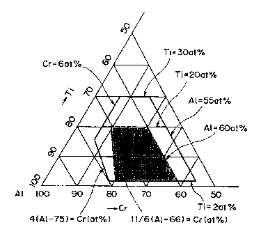
BRIEF DESCRIPTION OF THE DRAWINGS
Fig. 1 is a triangular diagram showing the amount of
metal components Ti, A1, and Cr in the (Ti, Al, Cr)N film.
Fig. 2 is a schematic diagram showing an example of
6a
CA 02366145 2001-12-24
the arc ion plating (AIP) apparatus used to practice the
present invention.
Fig. 3 is an enlarged schematic sectional diagram
showing the important part of the arc evaporating source
used to practice the present invention.
Fig. 4 is an enlarged schematic sectional diagram
showing the important part of another arc evaporating sour-
ce used to practice the present invention.
Fig. 5 is an enlarged schematic sectional diagram
showing the important part of a conventional arc evaporat-
ing source.
Fig. 6 is an X-ray diffraction pattern of a film hav-
ing a composition of (Tia,lAlo,,Cro,~)N. Part (1) is that of
the film formed by using the evaporating source of the
present invention. Part (2) is that of the film formed by
using the conventional evaporating source.
Fig. 7 is a graph showing the relation between the
substrate temperature and the residual stress in the film
having a composition of (Tio,lAlo,,Cro,2)N.
Fig. 8 is a diagram showing the range of the composi-
tion of metallic components Ti, A1, and Cr of (Ti,Al,Cr)N
film in Examples of the present invention.
Under the above-mentioned circumstances, the present
inventors conducted extensive studies to realize a hard
film for cutting tools which exhibits better wear resistan-
ce than before. As the result, it was found that the ob-
7
l~-
CA 02366145 2001-12-24
ject is achieved if the film has both improved hardness and
improved oxidation resistance. The present inventors con-
tinued their studies with their attention paid to TiAlN
film. It was found that the TiAlN film is greatly improved
in hardness and oxidation resistance and hence in wear
resistance if it is incorporated with Cr. It was also
found that, the TiAlN film is improved further in oxidation
resistance if it is incorporated with Si or B. Their quan-
titative investigations into the effect of these additives
led to the present invention.
The gist of the present invention resides in a hard
film composed of (T11_a-b-c-di Ala. Crb. Sia, Bd) (C1_aN,)
0.5 s a s 0.8, 0.06 s b, 0 s c s 0.1, 0 s d s 0.1,
0 s c+d s 0.1, a+b+c+d < 1, 0.5 s a s 1
(where a, b, c, and d denote respectively the atomic ratios
of A1, Cr, Si, and B, and a denotes the atomic ratio of N.)
A detailed description is given below of the composition of
the hard film.
TiAlN is a crystal of sodium chloride structure, or it
is a compound nitride of sodium chloride structure composed
of TiN in which the Ti site is replaced by A1. The fact
that A1N of sodium chloride structure is in an equilibrium
state at a high temperature under a high pressure suggests
that it has a high hardness. Therefore, it would be pos-
sible to increase the hardness of TiAlN film if the ratio
of A1 in TiAlN is increased, with its sodium chloride
structure maintained. However, A1N of sodium chloride
8
CA 02366145 2001-12-24
structure is in a nonequilibrium state at normal tempera-
ture under normal pressure or at a high temperature under a
low pressure. Consequently, ordinary gas-phase coating
merely forms A1N of ZnS structure (which is soft) and never
forms A1N of sodium chloride structure as a simple sub-
stance.
Nevertheless, it is possible to form TiAlN of sodium
chloride structure at normal temperature under normal pres-
sure ar at a high temperature under a low pressure, if
nitride film is formed by incorporation of A1 into Ti,
because TiN is of sodium chloride structure and has a lat-
tice constant close to that of A1N of sodium chloride
structure and hence A1N is assimilated into the structure
of TiN. However, as mentioned above, if the amount of A1
in TiAlN exceeds a certain limit which is defined by the
compos itional ratio ( x ) of 0 . 6-0 . 7 in ( AlX, Til_x ) N repre-
senting TiAlN, A1N of ZnS structure precipitates out be-
cause the effect of assimilation by TiN is weak.
Incidentally, it would be possible to increase the
ratio of A1N of sodium chloride structure further if Ti in
TiAlN is partly replaced by Cr, because CrN has a lattice
constant which is closer to that of A1N of sodium chloride
structure than that of TiN. If it is possible to increase
the ratio of A1N of sodium chloride structure in the film
by incorporation with Cr as mentioned above, it seems pos-
sible to make it harder than TiAlN film.
On the other hand, Japanese Patent Laid-open No.
9
i"'~.
CA 02366145 2001-12-24
310174/1995 discloses a method of increasing the hardness
and oxidation resistance of TiAlN by incorporation with Si.
The disclosed method requires that the amount of A1 be no
more than 0.75 (in atomic ratio) and the amount of Si be no
more than 0.1 (in atomic ratio). If the amounts of A1 and
Si exceed the above-specified limits, the resulting film
takes on the hexagonal crystal structure (which is soft).
Therefore, further improvement in oxidation resistance is
limited. By contrast, the present inventors found that it
is possible to increase both oxidation resistance and hard-
ness while maintaining the sodium chloride structure if the
TiAlN film is incorporated with not only Cr but also Si.
The behavior of Si is not yet elucidated; presumably, it
occupies the position of Ti. in the TiN lattice just as in
the case of A1 in TiAlN.
Incidentally, because A1N, CrN, and SiN excels TiN in
oxidation resistance, it is desirable to add A1, Cr, and Si
more rather than Ti from the view point of improving oxida-
tion resistance.
A detailed explanation is given below of the reason
why the atomic ratios a, b, c, d, and a have been estab-
lished for Ti, A1, Cr, Si, B, and C constituting the film
Of (Tll_,_b_~_d, A1,, Crb, 51~, Ba) (C1-vNo)
First, A1 should be added such that the lower limit
and the upper limit of its atomic ratio (a) is 0.5 and 0.8,
respectively, because a minimum amount of A1 is necessary
to secure oxidation resistance and hardness and an excess
CA 02366145 2001-12-24
amount of A1 precipitates soft hexagonal crystals, thereby
lowering the hardness of film.
Cr permits the A1 content to be increased while keep-
ing the sodium chloride structure as mentioned above. For
this effect, Cr should be added such that the lower limit
of its atomic ratio (b) is 0.06.
The atomic ratio (a) of A1 should be 0.55 or above,
preferably 0.60 or above. The lower limit of the atomic
ratio (b) of Cr should preferably be 0.08. In the case
where the atomic ratio (a) of A1 exceeds 0.765, the atomic
ratio (b) of Cr should preferably be within the range men-
tioned below. In addition, since CrN is less hard than TiN,
Cr will reduce hardness if added excessively. Thus, the
upper limit of the atomic ratio (b) of Cr should be 0.35,
preferably 0.3.
Fig. 1 is a triangular diagram showing the amount of
metal components Ti, Al, and Cr in the (Ti,Al,Cr)N film.
On the left-hand side of line b = 4(a - 0.75) or in the
area where b < 4(a - 0.75), the film hardness steeply de-
creases because A1N in the film contains crystals of ZnS
structure (which is soft) in higher ratio even though Cr is
added. Therefore, in the case where the atomic ratio (a)
of A1 exceeds 0.765, the ratio of Cr should preferably be
b Z 4(a - 0.75).
Si produces the effect of improving oxidation resis-
tance, as mentioned above. B also produces a similar ef-
fect. Therefore, Si andlor B should be added such that
11
CA 02366145 2001-12-24
their atomic ratio (c+d) is 0.01 or above, preferably 0.02
or above. On the other hand, excess Si and/or B separate
out in the form of soft hexagonal crystals, thereby impair-
ing wear resistance. Si and/or B should be added such that
the upper limit of their atomic ratios (c) and (d) or (c+d)
is 0.1, preferably 0.07 or less, more preferably 0.05 or
less.
Incidentally, silicon nitride forms a compact protec-
tive film of silicon oxide in an oxidizing atmosphere at
high temperatures, thereby protecting the coating film from
oxidation. On the other hand, boron nitride is inherently
superior in oxidation resistance (with its oxidation start-
ing at about 1000°C); however, its oxide is poor in pro-
tecting power once oxidation has started. That is to say,
boron is slightly inferior to silicon in oxidation resis-
tance. Therefore, it is desirable to add silicon alone
instead of adding silicon and boron in combination.
The amount of Ti is determined by the amount of Al, Cr,
Si, and B. TiN is harder than CrN, and the film will have
a low hardness if Ti is not added at all. Consequently, Ti
should be added such that the lower limit of its atomic
ratio (1-a-b-c-d) is 0.02, preferably 0.03. In the case
where the atomic ratio of A1 is 0.6 or above, the preferred
amount of Ti is such that its atomic ratio is 0.35 or less,
preferably 0.3 or less, because an excess amount of Ti
relatively decreases the amount of Cr, thereby reducing the
above-mentioned effect of assimilation.
12
CA 02366145 2001-12-24
Incidentally, in the case where Si and B are not con-
tained or the value of (c+d) is 0, the amount of Ti, A1,
and Cr should be such that the values of (a) and (b) are
within the range specified below.
0.02 s 1-a-b s 0.30, 0.55 s a s 0.765, 0.06 s b, or
0.02 s 1-a-b s 0.175, 0.765 s a, 4(a-0.75) s b.
If the atomic ratio of Ti is less than 0.20, the re-
sulting film has much improved oxidation resistance, with
the result that the temperature at which the film begins to
oxidize increases. Therefore, the values of (a) and (b) in
the range defined below is desirable.
0.02 s 1-a-b < 0.20, 0.55 s a s 0.765, 0.06 s b, or
0.02 s 1-a-b < 0.20, 0.765 s a, 4(a-0.75) s b.
If the atomic ratio (b) of A1 is 0.6 or above and the
upper limit of the atomic ratio (b) of A1 is such that the
resulting film is composed solely of crystals of sodium
chloride structure, the result is not only good oxidation
resistance but also higher hardness than Tio.,Alfl,6N would
have. ( It is to be noted that Tio,4Alo.6N has the highest
hardness among those compounds represented by TiAlN in
which 0.56 s A1 s 0.75).
Therefore, the most desirable range of (a) and (b) is
as follows.
0.02 s 1-a-b < 0.20, 0.60 s a s 0.709, or
0.02 s 1-a-b < 0.20, 0.709 s a, 11/6 x (a-0.66) s b.
The above-mentioned preferred range is recommended particu-
larly when the value of (c+d) is 0.
13
CA 02366145 2001-12-24
As in the case mentioned above, the upper limit of the
atomic ratio (b) of Cr should preferably be 0.35, prefera-
bly 0.3, because CrN is less hard than TiN and excessive Cr
lowers hardness.
Incorporation of C into the film causes hard carbides
(such as TiC, SiC, and BaC) to separate out, thereby making
the film harder. The amount (1 - e) of C should preferably
equal the total amount (1 - a - b) of Ti, Si, and B. Ex-
cessive C causes chemically unstable A1,C, and Cr,C, to
separate out, thereby deteriorating oxidation resistance.
Therefore, C should be added such that the value of (e) in
(Til_,_b_~~, Ala, Crb, Si~, Bd) (C1_oN,) is 0.5 or above, prefera-
bly 0.7 or above, more preferably 0.8 or above, and most
desirably 1.
Incidentally, the hard film of the present invention
should preferably be composed mainly of crystals of sodium
chloride structure, because it loses high strength if it
contains crystals of ZnS structure.
The crystal in which the sodium chloride structure
dominates is one which has the peak intensity of X-ray
diffraction (8-28 method) defined by expression (4) below,
whose value is 0.5 or above, preferably 0.8 or above.
[IB(111)+IB(200)+IB(220)+IB(311)+IB(222)+IB(400)]/
[IB(111)+IB(200)+IB(220)+IH(311)+IB(222)+IB(400)+
IH(100)+IH(102)+IH(110)] ... (4)
(where IB(111), IB(200), IB(220), IH(311), IB(222), and
IB(400) represent respectively the peak intensity due to
14
CA 02366145 2001-12-24
(111) plane, (200) plane, (220) plane, (311) plane, (222)
plane, and (400) plane of sodium chloride structure, and
IH(100), IH(102), and IH(110) represent respectively the
peak intensity due to (100) plane, (102) plane, and (110)
plane of ZnS structure.)
If the value of expression (4) is less than 0.5, the re-
sulting film has a hardness lower than that which is re-
garded as desirable in the present invention.
The peak intensity of ZnS structure is measured by
using an X-ray diffractometer which emits Cu Ka line. The
peak intensity is one which appears at 28 = 32-33° for
(100) plane, at 28 = 48-50° for (102) plane, or at 28 =
57-58° for (110) plane. Incidentally, although the crystal
of ZnS structure is composed mainly of A1N, its peak posi-
tion actually measured is slightly different from that
shown in JCPDS cards because it contains Ti, Cr, Si, and B.
The film of the present invention should preferably
have the sodium chloride structure such that the peak in-
tensity measured by X-ray diffraction satisfies the follow-
ing. I(220) s I(111) and/or I(220) s I(200) The reason
for this is that the film has good wear resistance when the
(111) plane or (200) plane (which is the closely packed
plane of sodium chloride structure) is parallel to the film
surface.
The ratio of I(200)/I(111) should preferably be 0.1 or
above (where I(200) denotes the peak intensity due to (200)
plane and I(111) denotes the peak intensity due to (111)
CA 02366145 2001-12-24
plane). This ratio varies in the range of about 0.1 to 5
depending on film-forming conditions, such as bias voltage
applied to the substrate, gas pressure, and film-forming
temperature. It was found in this invention that the film
exhibits good cutting characteristics when the ratio is 0.1
or above. A probable reason for this is as follows. It is
considered. that in the crystal of sodium chloride structure,
metal elements basically combine with nitrogen or carbon
and there are very few metal-metal bonds, nitrogen-nitrogen
bonds, and carbon-carbon bonds. Thus, metal atoms adjoin
metal atoms, nitrogen atoms adjoin nitrogen atoms, and car-
bon atoms adjoin carbon atoms in the (111) plane, whereas
metal atoms adjoin nitrogen atoms or carbon atoms in the
(200) plane. There is a high possibility that metal atoms
combine with nitrogen atoms or carbon atoms in the (200)
plane, and this leads to a good stability. Thus, it is
expected that if the stabler (200) plane is oriented at a
certain ratio with respect to the (111) plane, the result-
ing film has increased hardness and exhibits improved cut-
ting characteristics. The value of I(200)/I(111) should be
0.3 or above, preferably 0.5 or above.
The angle of diffraction due to (111) plane varies
depending on the film composition, the state of residual
stress, and the kind of substrate. The results of X-ray
diffraction (A-2A method) with Cu Ka line indicate that the
hard film of the present invention varies in the angle of
diffraction in the range of about 36.5-38.0° and that the
16
CA 02366145 2001-12-24
angle of diffraction tends to decrease as the amount of Ti
increases in the film. A probable reason why the angle of
diffraction due to (111) plane decreases (or the distance
between (111) planes increases) with the increasing amount
of Ti in the film is that the lattice constant (4.24A) of
TiN is larger than the lattice constant (4.12A) of A1N and
the lattice constant (4.14A) of CrN of sodium chloride
structure, as mentioned above. Incidentally, when the hard
film of the present invention, which has the composition of
(Tia.l2Alo_,oCro,lSSio.o3)N. was formed on a cemented carbide
substrate, the angle of diffraction due to (111) plane
varies in the range of 36.6-37.1° depending on the film-
forming conditions.
The angle of diffraction due to (111) plane of sodium
chloride structure can be calculated from the following
Bragg's formula (5).
2 x (spacing of lattice planes, A) x sin (angle of diffrac-
tion 28/2) = wavelength of X-rays used (A) ... (5)
The wavelength of X-rays is 1.54056A for Cu Ka line.
Incidentally, the spacing of (111) planes in expression (5)
can be calculated from the following expression (6) which
is obtained by using the law of mixture from the standard
lattice constants (4.24A, 4.12A, and 4.14A) and the compo-
sitional ratio of TiN, A1N, and CrN of sodium chloride
structure.
Spacing of (111) planes (A) - [2.4492 x Ti (at%) + 2.379 x
A1 (at%) + 2.394 x Cr (at%)]/100 ... (6)
17
CA 02366145 2001-12-24
(The amount of each element is expressed in terms of 100%
metallic element.)
In the case where the hard film of the present inven-
tion, which has the composition of (Tio,lAla,,2Cro.lB)N, is
formed on a cemented carbide substrate, the angle of dif-
fraction obtained from the above-mentioned expression (5)
is 37.6°. ,In actual, however, the angle of diffraction
varies in the range of 37.2-37.7° depending on the film-
forming conditions and residual stress. The hard film of
the present invention in its as-formed state receives com-
pressive stress and hence the spacing of lattice planes
parallel to the substrate is larger (due to Poisson effect)
than that in the normal state or that calculated form the
above-mentioned expression (6). Therefore, the angle of
diffraction due to (111) plane measured by X-ray diffrac-
tion (A-28 method) was smaller than that in the normal
state or that calculated from the above-mentioned expres-
sion (5) by substituting the spacing of lattice plane in
the normal state obtained from the above-mentioned expres-
sion (6).
It is desirable that the angle of diffraction'due to
(111) plane obtained by X-ray diffraction (A-28 method)
with Cu Ka line should~be within ~0.3° of the standard
angle of diffraction which is calculated from the above-
mentioned expressions (5) and (6) on the basis of the com-
position of metallic elements in the film.
The diffraction peak due to (111) plane has the prop-
18
CA 02366145 2001-12-24
erty that its half width varies depending on crystal size
in the film and non-uniform residual stress in the film and
crystals in the film tend to become small as the half width
increases. [Half width usually denotes FWHM (Full Width
Half Maximum) which is the width of that part of diffrac-
tion peak at which the intensity is half the maximum inten-
sity of the diffraction peak.] This half width is about
from 0.2° to 1° in the case of the hard film which satisfi-
es the requirements of the present invention. In the case
of hard f ilm represented by ( Tio, lAlo. "Cro.le ) N ( mentioned
above), the half width ranges from 0.3° to 0.8° depending
on the film-forming conditions.
The hard film of the present invention may be used in
the form of single-layer film which meets the above-men-
tioned requirements. It may also be used in the form of
mufti-layer film, each layer being mutually different and
satisfying the above-mentioned requirements. The
(Ti,Cr,Al,Si,B)(CN) film specified in the present invention,
which is in the form of single layer or multiple layers,
may have on its one side or both sides at least one layer
composed of crystals in which the sodium chloride structure
dominates, which is selected from the group consisting of a
layer of metal nitride, a layer of metal carbide, and a
layer of metal carbonitride (which differ from the above-
mentioned hard film in composition).
Incidentally, the ~~crystal in which the sodium chlo-
ride structure dominates" denotes the same one as defined
19
CA 02366145 2001-12-24
above, which has the peak intensity of X-ray diffraction
(8-2A method) defined by expression (4) given above, whose
value is 0.8 or above. (with IB(111), IB(200), IB(220),
IB(311), IB(222), and IB(400) representing respectively the
peak intensity due to (111) plane, (200) plane, (220) plane,
(311) plane, (222) plane, and (400) plane of sodium chlo-
ride structure, and IH(100), IH(102), and IH(110) repre-
senting respectively the peak intensity due to (100) plane,
(102) plane, and (110) plane of ZnS structure.) The layers
of metal nitride, metal carbide, and metal carbonitride
(which are of sodium chloride structure and differ from the
above-mentioned hard film in composition) include, for
example, those films of TiN, TiAlN, TiVAIN, TiCN, TiAICN,
TiNbAICN, and TiC.
The hard film for cutting tools according to the pre-
sent invention may have on its one side or both sides, in
addition to the above-mentioned one or more layers, one or
more layers of metal or alloy containing at least one metal
selected from the group consisting of 4A Group elements, SA
Group elements, 6A Group elements, A1, and Si. The metals
belonging to 4A Group, 5A Group, and 6A .Group include Cr,
Ti, and Nb. The alloy includes Ti-A1. Such laminated film
structure is effective for substrates made of ferrous mate-
rial (such as HSS and SKD) which are inferior to those of
cemented carbide in adhesion to the hard film. The hard
film with good adhesion to the substrate is obtained by
sequentially forming on the above-mentioned ferrous sub-
CA 02366145 2001-12-24
strate the above-mentioned film of Cr, TiN, or TiAlN (which
is less hard than the hard film specified in the present
invention), an intermediate metal layer of Cr, Ti, or Ti-A1,
and the hard film of the present invention. The intermedi-
ate layer which is relatively softer than the hard film of
the present invention reduces residual stress, thereby
improving adhesion (peel resistance).
In the case where the hard film of the present inven-
tion consists of more than one layer, each layer may have a
thickness in the range of 0.005-2 ~,m; however, the hard
film of the present invention should preferably have a
total thickness of from 0.5 N,m to 20 ~,m regardless of
whether it is of single-layer structure or composed of more
than one layer. The multiple-layer structure may be formed
from (i) mutually different films each satisfying the re-
quirements of the present invention, (ii) layers of metal
nitride, metal carbide, or metal carbonitride which are of
sodium chloride structure and different from the above-
mentioned hard film in composition, and (iii) layers of
metal or alloy containing at least one metal selected from
the group consisting of 4A Group elements, 5A Group ele-
ments, 6A Group elements, A1, and Si. With a total thick-
ness less than 0.5 Vim, the resulting hard film is too thin
to have sufficient wear resistance. With a total thickness
more than 20 ~.i,m, the resulting hard film is liable to break
or peel during cutting. Therefore, a more preferable
thickness is 1 ~m or more and 15 N,m or less.
21
CA 02366145 2001-12-24
Incidentally, the cutting tools to be coated with the
hard film of the present invention include end mills,
drills, hobs, and throw-away inserts which are made of
cemented carbide, high speed steel (HSS), cermet, or CBN
sintered body. Recently, cutting tools are used under
severer conditions than before as the work becomes harder
and the cutting speed increases, and hence the coating film
for them is required to have higher hardness and better
oxidation resistance. The hard film of the present inven-
tion satisfies both of these requirements. It is most
suitable for those cutting tools which are used under dry
or semi-dry cutting conditions. The conventional typical
film of TiAlN does not exhibit sufficient oxidation resis-
tance and hardness under dry cutting conditions (in which
the temperature is considerably high). This drawback is
overcome by the film of the present invention which has
both high hardness and good oxidation resistance.
The film of the present invention, whose crystal
structure is dominated substantially by sodium chloride
structure despite its high A1 content, may be formed effec-
tively by the process specified in the present invention.
This process consists of vaporizing and ionizing a metal
constituting a target by arc discharge in a film-forming
gas atmosphere and converting said metal and film-forming
gas into a plasma, thereby forming a film. The process
should preferably be carried out in such a way as to accel-
22
CA 02366145 2001-12-24
erate the conversion of film-forming gas into a plasma by
the magnetic lines of force which:
a) are parallel to the normal at the target's evapo-
rating surface, and
b) run toward the substrate in the direction parallel
to or slightly divergent from the normal to the target's
evaporating surface.
The arc ion plating (AIP) apparatus used in the proc-
ess of the present invention differs from the conventional
one, in which the source of magnetic field is placed behind
the target and the component of magnetic field perpendicu-
lar to the target film is small. The apparatus used to
form the hard film of the present invention is constructed
such that the magnet is placed beside or in front of the
target so that magnetic lines of force diverge approxi-
mately perpendicularly to or extend parallel to the evapo-
rating surface of the target. The magnetic lines of force
accelerate the conversion of the film-forming gas into a
plasma. This is very effective in forming the hard film of
the present invention.
An example of the AIP apparatus used to practice the
present invention is shown in Fig. 2. A brief description
of the AIP apparatus is given below.
The AIP apparatus consists of a vacuum chamber 1
(which has an evacuating port 11 connected to a vacuum pump
and a supply port 12 to feed a film-forming gas), an arc-
vaporizing source 2 which vaporizes and ionizes by arc
23
CA 02366145 2001-12-24
discharge a target constituting a cathode, a holder 3 to
hold a substrate W (cutting tool) to be coated, and a bias
power source 4 to apply through the holder 3 a negative
bias voltage to the substrate W across the holder 3 and the
vacuum chamber 1.
The arc-vaporizing source 2 is provided with a target
6 constituting a~cathode, an arc power source 7 connected
to the target 6 and the vacuum chamber 1 constituting an
anode, and a permanent magnet 8 to generate a magnetic
field forming magnetic lines of force which diverge ap-
proximately perpendicularly to or extend parallel to the
evaporating surface of the target and reach the vicinity of
the substrate W. The magnetic field should be such that
its magnetic flux density is higher than 10 G (Gauss),
preferably higher than 30 G, at the center of the substrate.
Incidentally, the term "approximately perpendicularly to
the evaporating surface" means an angle of from 0° to about
30° with respect to the normal to the evaporating surface.
Fig. 3 is an enlarged sectional schematic diagram
showing the important part of the arc evaporating source
used to practice the present invention. The above-men-
tioned magnet 8 to generate a magnetic field is so arranged
as to surround the evaporating surface S of the target 6.
The magnet is not a sole means to generate a magnetic
field; it may be replaced by an electromagnet consisting of
a coil and an electric source. Alternatively, the magnet
may be so placed as to surround the front (facing the sub-
24
CA 02366145 2001-12-24
strate) of the evaporating surface S of the target 6, as
shown in Fig. 4. Incidentally, although the vacuum chamber
in Fig. 1 functions as an anode, it is also possible to
provide a special cylindrical anode which surrounds the
side front of the target.
Incidentally, Fig. 5 shows a conventional AIP appara-
tus, in which the arc evaporating source 102 is provided
with an electromagnet 109 to concentrate the arc discharge
onto the target 106. However, since the electromagnet 109
is placed behind the target 106, the magnetic lines of
force become parallel to the target surface in the vicinity
of the target evaporating surface and hence do not reach
the vicinity of the substrate W.
The arc evaporating source of the AIP apparatus used
in the present invention differs from the conventional one
in the structure of magnetic field and hence in the way the
plasma of film-forming gas expands.
The evaporating source shown in Fig. 4 converts the
film-forming gas into plasma as the result of arc-induced
electrons (e) partly winding around the magnetic line of
force and colliding with nitrogen molecules constituting
the film-forming gas. By contrast, the conventional evapo-
rating source 102 shown in Fig. 5 works differently. That
is, the magnetic lines of force are confined near the tar-
get and hence the plasma of film-forming gas generated as
mentioned above has the highest density near the target and
a low density near the substrate W. However, in the case
CA 02366145 2001-12-24
of the evaporating source shown in Figs. 3 and 4, which is
used in the present invention, the magnetic line of force
reach the substrate W, so that the plasma of film-forming
gas has a much higher density near the substrate W than
that in the case of conventional evaporating source. It is
considered that the different in plasma density affects the
crystal structure of the film formed.
An example of such effects actually observed is shown
in Fig. 6, which is an X-ray diffraction pattern of a Ti-
CrAlN film (having a composition of (Tia,lCra_ZAlo.,)N) which
was prepared by using the conventional evaporating source
and the improved evaporating source of the present inven-
tion. In Fig. 6 "B1" represents the sodium chloride struc-
ture and "Hex" represents the Zns structure and "( )" rep-
resents the crystal plane. In addition, unmarked peaks in
Fig. 6 are ascribed to the substrate (cemented carbide).
Both of the evaporating sources were operated to form film
samples under the following conditions. Arc current: 100A,
pressure of nitrogen gas: 2.66 Pa, substrate temperature:
400°C, and bias voltage for substrate: varied from 50V to
300V. Incidentally, the bias voltage is negative with
respect to earth potential. Thus, a bias voltage of 100V,
for example, means a bias voltage which is -100V with re-
spect to earth potential.
The evaporating source of the conventional AIP appara-
tus, in which the magnet is placed behind the target,
yields a film which is composed of mixed phases of cubic
26
CA 02366145 2004-11-22
system (sodium chloride structure) and hexagonal system
(ZnS structure) even when the bias voltage is increased to
300V, as shown in Fig. 6(B). By contrast, the evaporating
source of the AIP apparatus of the present invention, in
which the magnet is placed beside the target, yields a film
which is composed of single phase of sodium chloride struc-
ture when the bias voltage is 70V or higher with respect to
earth potential, as shown in Fig. 6(A).
A1N of sodium chloride structure is inherently in a
non-equilibrium state at normal temperature under normal
pressure, and hence it is a substance which does not form
readily. Nevertheless, it is considered that the evaporat-
ing source of the present invention actively converts ni-
trogen into plasma and the resulting high-energy nitrogen
particles help to form the A1N of sodium chloride structure
in a non-equilibrium state.
The higher is the bias voltage, the higher becomes the
energy of film-forming gas and metal ions which have been
converted into plasma, and the crystals of the film take on
sodium chloride structure more readily. Consequently, the
bias voltage should be 50V or higher, preferably 70V or
higher, and more preferably 100V or higher. However, an
excessively high bias voltage is not practical because the
film is etched by the film-forming gas which has been con-
verted into plasma and hence the film-forming rate is ex-
tremely small. Consequently, the bias voltage should be
400V or lower, preferably 300V or lower, more preferably
27
CA 02366145 2001-12-24
260V or lower, and most desirably 200V or lower. Inciden-
tally, the bias voltage is negative with respect to earth
potential. Thus, a bias voltage of 100V, for example,
means a bias voltage which is -100V with respect to earth
potential. The object of applying a bias voltage is to
impart energy to the incident film-forming gas and metal
ions from the target, thereby allowing the film to take on
the sodium chloride structure. The preferred range of the
bias voltage varies depending on the composition of the
film to be formed. In the case of film with a compara-
tively low A1 content or a comparatively high Cr content, a
comparatively low bias voltage will work owing to the
above-mentioned assimilating effect which contribute to
sodium chloride structure. If the A1 content is less than
about 65 atom% or the Cr content is more than about 25
atom%, it is possible to obtain a single-layer film of
sodium chloride structure even when the bias voltage is 70V
or lower.
According to the present invention, the substrate tem-
perature should be in the range of 300-800°C at the time of
film forming. This is related with the stress of the re-
sulting film.
Fig. 7 is a graph showing the relation between the
substrate temperature and the residual stress of the re-
sulting film having a composition of (Tio.lAlo_,Cro,2)N. The
film was formed under the following conditions. Arc cur-
rent: 100A, bias voltage for the substrate: 150V, and pres-
28
CA 02366145 2001-12-24
sure of nitrogen gas: 2.66 Pa.
It is noted from Fig. 7 that the residual stress in
the resulting hard film decreases according as the sub-
strate temperature increases. The resulting film with
excessive residual stress is poor in adhesion and liable to
peeling. Consequently, the substrate temperature should be
300°C or higher, preferably 400°C or higher. On the other
hand, the higher the substrate temperature, the less the
residual stress. However, the film with excessively small
residual stress is poor in compressive strength and hence
less effective in increasing the resistance of the sub-
strate to bending. It also causes thermal change to the
substrate due to high temperature. Consequently, the sub-
strate temperature should be 800°C or lower, preferably
700°C or lower.
In the case where the substrate is cemented carbide,
the above-mentioned substrate temperature is not specifi-
cally restricted. However, in the case where the substrate
is high speed tool steel (such as JIS-HSS and JIS-SKH51)
and hot work tool steel (such as JIS-SKD11 and JIS-SKD61),
the substrate temperature at the time of film forming
should be lower than the tempering temperature so that the
substrate retains its mechanical properties. The tempering
temperature varies depending on the substrate material; it
is about 550-570°C for JIS-SKH51, 550-680°C for JIS-SKD61,
and 500-530°C for JIS-SKD11. The substrate temperature
should be lower than the tempering temperature, preferably
29
CA 02366145 2001-12-24
lower than the tempering temperature by about 50°C.
According to the present invention, the film should
preferably be formed such that the reactant gas has a par-
tial pressure or total pressure in the range of from 0.5 Pa
to 7 Pa. The pressure of the reactant gas is expressed in
terms of "partial pressure or total pressure" because the
reactant gas may or may not contain an assist gas. The
reactant gas without assist gas is nitrogen or methane
which contains elements essential for the film. The assist
gas is a rare gas such as argon. In the case where the
film is formed from the reactant gas without assist gas, it
is necessary to control the total pressure of the reactant
gas. In the case where the film is formed from the reac-
tant gas with an assist gas, it is necessary to control the
partial pressures of both the reactant gas and the assist
gas. If the partial pressure or total pressure of the
reactant gas is lower than 0.5 Pa, evaporation by arc gives
rise to a large amount of macroparticles (resulting from
molten target), making the film surface rough, which is
undesirable for some applications. On the other hand, if
the partial pressure or total pressure of the reactant gas
is higher than 7 Pa, the reactant gas scatters evaporated
particles due to frequent collision, thereby lowering the
film-forming rate. Therefore, the partial or total pres-
sure of the reactant gas should be from 1 Pa to 5 Pa, pref-
erably from 1.5 Pa to 4 Pa.
In the present invention, the AIP method is used for
CA 02366145 2001-12-24
film forming, and it has been explained above. The film-
forming method is not restricted to AIP; any method can be
used so long as it efficiently converts the metallic ele-
ments and the reactant gas into plasma. Such additional
methods include pulse sputtering and nitrogen ion beam
assisted deposition.
The hard film of the present invention may be effec-
tively produced by vapor-phase coating such as ion-plating
and sputtering in which a target is vaporized or ionized so
as to form a film on the substrate, as mentioned above.
Any target lacking desirable properties does not permit
stable discharging at the time of film forming; therefore,
the resulting film is poor in the uniformity of composition.
The present inventors' investigation on the target proper-
ties necessary for the hard film with good wear resistance
revealed the following.
First, the target should have a relative density not
lower than 95%. This condition is necessary to provide
stable discharging at the time of film forming and to effi-
ciently yield the hard film of the present invention. With
a relative density lower than 95%, the target has a coarse
portion such as micropores in the alloy component. A tar-
get with such an alloy component does not evaporate uni-
formly, and hence the resulting film varies in composition
and thickness. In addition, porous portions consume local-
ly and rapidly, thereby reducing the target life. A target
with a large number of voids not only rapidly consumes but
31
CA 02366145 2001-12-24
also cracks due to loss of strength. The relative density
of the target should preferably be 96% or higher, more
preferably 98% or higher.
Even though a target has a relative density not lower
than 95%, it may not yield a good film (due to unstable
discharging) if it has large voids. It is known that a
target with voids larger than 0.5 mm in radius does not
permit continuous film forming because arc discharging is
interrupted by the alloy component evaporating or ionizing.
The present inventors' investigation revealed that dis-
charging is unstable, although not interrupted, if there
are voids not smaller than 0.3 mm in radius. Therefore,
for stable discharging and efficient satisfactory film
forming, it is desirable that voids in a target should be
smaller than 0.3 mm in radius, preferably 0.2 mm or smaller
in radius.
In vapor phase coating by the AIP method, the composi-
tion of the target used determines the composition of the
film formed. Therefore, it is desirable that the composi-
tion of the target should be identical with the composition
of the intended film. In order to obtain the hard film of
the present invention which is superior in wear resistance,
it is necessary to employ a target having the composition
Of (Tli_x_Y_$-.,, Alx, Cry, $7.a, Bv)
0.5 s x s 0.8, 0.06 s y, 0 s z s 0.1, 0 s w s 0.1,
0 s z+w s 0.1, x+y+z+w < 1
(where x, y, z, and w denote respectively the atomic ratios
32
CA 02366145 2001-12-24
of A1, Cr, Si, and B. This is to be repeated in the fol-
lowing.)
In the case where the hard film of the present inven-
tion does not contain Si and B, the values of x, y, z; and
w should preferably be in the range defined below.
0.02 s 1-x-y s 0.30, 0.55 s x s 0.765, 0.06 s y, z+w = 0,
or 0.02 s 1-x-y s 0.175, 0.765 s x, 4(x-0.75) s y, z+w = 0.
In addition to meeting the above-mentioned require-
ments for composition, the target should have a uniform
distribution of composition. Otherwise, the resulting hard
film lacks uniformity in the distribution of composition
and hence varies in wear resistance from one part to an-
other. In.addition, a target with varied distribution of
composition suffers local variation in electrical conduc-
tivity and melting point. This leads to unstable discharg-
ing and hence to a poor film. Consequently, the target of
the present invention should have a uniform distribution of
composition whose variation is within 0.5 atom%.
The present inventors also investigated how the dis-
charging state at the time of film forming varies depending
on the amount of inevitable impurities (such as oxygen,
hydrogen, chlorine, copper, and magnesium) entering the
target from the raw material or the atmosphere in which the
target is produced.
As the result it was found that a target containing
oxygen, hydrogen, and chlorine in large amounts explosively
releases these gases, resulting in unstable discharging and,
33
CA 02366145 2001-12-24
in the worst case, breaking itself, making film forming
impossible. Therefore, it is desirable that the target
contain oxygen, hydrogen, and chlorine in a limited amount
not more than 0.3 mass%, 0.05 mass%, and 0.2 mass%, respec-
tively. The preferred content of oxygen, hydrogen, and
chlorine should be not more than 0.2 mass%, 0.02 mass%, and
0.15 mass%, respectively.
Copper and magnesium are also detrimental impurities
because they are more volatile (with a higher vapor pres-
sure) than Ti, A1, Cr, Si, and B constituting the target of
the present invention. When contained in large amounts,
they form voids in the target at the time of film forming,
and such voids make discharging unstable during film form-
ing. Therefore, the content of copper in a target should
be 0.05 mass% or less, preferably 0.02 mass% or less. The
content of magnesium in a target should be 0.03 mass% or
less, preferably 0.02 mass% or less.
One way to reduce the content of impurities as speci-
fied above is by vacuum melting of raw material powder or
by mixing of raw material powder in a clean atmosphere.
In the meantime, the present invention does not speci-
fy the method of preparing the target. However, there is a
preferred method which consists of uniformly mixing raw
material powers in an adequate ratio by using a V-blender
or the like and then subjecting the resulting mixture to
CIP (cold isostatic pressing) or HIP (hot isostatic press-
ing). The raw material powder is composed of Ti powder, Cr
34
CA 02366145 2001-12-24
powder, A1 powder, Si powder, and B powder which have an
adequately controlled particle size. Other methods include
hot extrusion and super-high pressure hot pressing.
Although it is possible to produce a target from the
mixed powder by hot pressing (HP), the resulting target
does not have a sufficiently high relative density because
Cr is a high-melting metal. Instead of producing a target
from a mixed powder as mentioned above, it is also possible
to produce a target from a previously alloyed powder, by
means of CIP or HIP, or through melting and solidifying.
The CIP or HIP with an alloy powder offers the advantage
that the resulting target has a uniform composition; how-
ever, it also suffers the disadvantage that the resulting
target tends to have a low relative density because the
alloy powder is poor in sinterability. The method involv-
ing the melting and solidifying of an alloyed powder offers
the advantage that the resulting target has a comparatively
uniform composition but has the disadvantage that the re-
sulting target is subject to cracking and shrinkage cavity
at the time of solidification. It does not easily yield
the target of the present invention.
The invention will be described in more detail with
reference to the following examples, which are not intended
to restrict the scope thereof. Various changes and modifi-
cations may be made to the examples without departing from
the spirit and scope of the invention.
,,~...
CA 02366145 2001-12-24
Example 1
A target of alloy composed of Ti, Cr, and A1 was
mounted on the cathode of the AIP apparatus shown in Fig. 2.
A substrate was mounted on the holder. The substrate is a
chip of cemented carbide, a square end mill of cemented
carbide (10 mm in diameter, with two edges), or a piece of
platinum foil (0.1 mm thick). The chamber was evacuated to
a degree of vacuum lower than 3 x 10-' Pa while the sub-
strate was being heated to 400°C by means of a heater
placed in the chamber. The substrate was given a bias
voltage of 700V in an argon atmosphere at 0.66 Pa, so that
the substrate was cleaned with argon ions for 10 minutes.
Subsequently, nitrogen gas was introduced into the chamber.
With the chamber pressure kept at 2.66 Pa, an arc current
of 100A was applied for film forming. A 4-~.im thick film
was formed on the surface of the substrate. Incidentally,
a bias voltage of 150V was applied to the substrate so that
the substrate was kept negative with respect to earth po-
tential during film forming.
After the film-forming step was complete, the result-
ing film was examined for composition of metal components,
crystal structure, Vickers hardness, and oxidation starting
temperature. Vickers hardness was measured by using a
microvickers tester under a load of 0.25N for 15 seconds.
The composition of Ti, Cr, and A1 in the film was deter-
mined by EPMA. The content of metal elements and impurity
elements (such as O and C, excluding N) in the film was
36
CA 02366145 2001-12-24
also determined by EPMA. It was found that the content of
oxygen is less than 1 atom% and the content of carbon is
less than 2 atom%. The crystal structure of the film was
identified by X-ray diffraction. The oxidation starting
temperature was measured as follows by using the platinum
sample. The platinum sample was heated in a dry air from
room temperature at a rate of 5°C/min by using a thermobal-
ance. The temperature at which the weight changes is meas-
ured and it is regarded as the oxidation starting tempera-
ture. The value in the foregoing expression (4) was ob-
tained by measuring the intensity of peaks due to respec-
tive crystal planes by using an X-ray diffractometer with
Cu Ra line. Table 1 shows the thus obtained results (in-
cluding composition of film, crystal structure, Vickers
hardness, oxidation starting temperature, and the value of
expression (4)).
37
CA 02366145 2001-12-24
Table 1
Exper-Metals Vickers ~idation Crystal Value
in of
film
(atomic
ratio)
invent starting * expres-
No. Ti Cr pi hardness tem- structurelion
stature 4
C
1 0.27 0.07 0.66 3090 850 B1 1
2 0.21 0.08 0.71 3010 880 B1+Hex 0.83
3 0.19 0.07 0.74 2960 900 B 1 +H 0.81
ex
4 0.09 0.15 0.76 2950 920 B 1 +H 0.86
ex
0.02 0.19 0.79 2900 960 B1+Hex 0.82
6 0.18 0.12 0.70 3300 880 B1 1
7 0.09 0.19 0.72 3500 910 B1 1
8 0.04 0.21 0.75 3300 940 B1 1
9 0.28 0.12 0.60 3080 850 B1 1
0.18 0.20 0.62 3200 870 B1 1
11 0.11 0.22 0.67 3340 890 B1 1
12 0.10 0.28 0.62 3130 870 B1 1
13 0.04 0.28 0.68 3210 910 B 1 1
14 0.04 0.33 0.63 3110 880 B 1 1
0.17 0.25 0.58 3050 860 B1 1
16 0.10 0.34 0.56 3020 860 B1 1
17 0.04 0.38 0.58 3030 870 B1 1
18 0.32 0.10 0.58 2870 830 B1 1
19 0.22 0.26 0.52 2920 830 B1 1
0.04 0.43 0.53 2820 840 B1 1
21 0.44 0 0.56 2700 800 B1 1
22 0.40 0 0.60 3050 820 B1 1
23 0.25 0 0.75 2700 850 B1 1
24 0.17 0.05 0.78 2300 900 B1+Hex 0.55
0.10 0.10 0.80 2200 930 Bt+Hex 0.35
26 0.03 0.17 0.80 2500 960 B 1 +H 0.75
ex
i 27 - O -- - 0.75~ -2650 950 B1 1
~ I x.25 --
--
~
* B1 represents sodium chloride structure, and Hex represents ZnS structure.
38
CA 02366145 2001-12-24
It is noted from Table 1 that the samples of TiAlN
(0.56 s A1 s 0.75) in Experiment Nos. 21, 22, and 23 have a
film hardness of 2700-3050 and an oxidation stating tem-
perature of 800-850°C. However, they do not have both
improved film hardness and oxidation starting temperature.
By contrast, the samples of Experiment Nos. 1 to 17, which
have the composition as specified in the present invention,
have a high Vickers hardness as well as a high oxidation
starting temperature.
The composition for metal components Ti, A1, and Cr in
the (Ti,Al,Cr)N film is shown in Fig. 8. Each composition
is indicated by the sample No. (1 to 27). Samples Nos. 1
to 17 (marked with ~, ~, and ~ ) , which are within the
range specified by the present invention, has both the high
hardness and the high oxidation starting temperature char-
acteristic of TiAlN (0.56 s A1 s 0.75). In particular,
samples Nos. 3 to 5 (marked with ~), which have a composi-
tion within the desirable range, have a high oxidation
starting temperature, which is almost comparable to that of
TiAlN (0.56 s A1 s 0.75) and also has a very high hardness.
Samples Nos. 15 to 17 have a hardness equivalent to the
highest hardness of TiAlN (0.56 s A1 s 0.75) and also a
high oxidation starting temperature.
Samples Nos. 6 to 9 and 10 to 14 (marked With ~),
which have a composition within the desirable range, has
the highest hardness and the highest oxidation starting
temperature which have never been attained by the conven-
39
CA 02366145 2001-12-24
tional TiAlN (0.56 s A1 s 0.75) film. They exhibit better
wear resistance than the conventional TiAlN (0.56 s A1 s
0.75) film.
By contrast, samples Nos. 18 to 20 and 24 to 27
(marked with O), which have a composition outside the
range specified in the present invention, do not have a
high hardness and a high oxidation starting temperature at
the same time. They are equivalent to or inferior to the
conventional TiAlN (0.56 s A1 s 0.75) film and hence they
are not expected to have better wear resistance than the
conventional TiAlN (0.56 s A1 s 0.75) film.
Example 2
Samples Nos. 1, 4, 7, 11, 16, 18, 19, 22, 24, and 27
in Example 1, which are end mills coated with the hard film,
were tested for wear resistance by cutting several works of
quenched JIS-SKD61 (HRC50) under the following conditions.
Cutting speed: 200 m/min
Feed speed: 0.07 mm/edge
Depth of cut: 5 mm
Pick feed: 1 mm
Cutting oil: air blow only
Cutting direction: down cutting
After cutting over a length of 20 meters, the cutting edge
of the end mill was examined under an optical microscope to
measure the worn width. The results are shown in Table 2.
CA 02366145 2001-12-24
Table 2
Experiment Wom width
No. (gym)
1 38
4 32
7 24
11 26
i6 33
18 59
19 55
22 48
24 73
27 - 62 _
It is noted from Table 2 that the samples of end mills Nos.
1, 4, 7, 11 and 16, which are coated with the film meeting
the requirements of the present invention, are superior in
wear resistance (in terms of worn width) to the samples Nos.
18, 19, 22, 24, and 27, which are coated with the film not
meeting the requirements of the present invention.
A target of alloy composed of Ti, Cr, Al, and Si was
mounted on the cathode of the AIP apparatus shown in Fig. 2.
A substrate was mounted on the holder. The substrate is a
chip of cemented carbide, a square end mill of cemented
carbide (10 mm in diameter, with four edges), or a piece of
platinum foil (0.2 mm thick). The chamber was evacuated to
a degree of vacuum lower than 3 x 10'' Pa while the sub-
strate was being heated to 550°C by means of a heater
placed in the chamber. The substrate was cleaned with
argon ions for 10 minutes. Subsequently, nitrogen gas or a
41
CA 02366145 2001-12-24
mixture gas of nitrogen and methane was introduced into the
chamber. With the chamber pressure kept at 2.66 Pa, an arc
current of 100A was applied for film forming. An approxi-
mately 3-hum thick film was formed on the surface of the
substrate. Incidentally, a bias voltage of 100-200v was
applied to the substrate so that the substrate was kept
negative with respect to earth potential during film form-
ing.
After the film-forming step was complete, the result-
ing film was examined for composition of metal components,
crystal structure, Vickers hardness, and oxidation starting
temperature. The composition of Ti, Cr, A1, and Si in the
film was determined by EPMA (with mass absorption coeffi-
cient corrected). The content of metal elements and impu-
rity elements (such as O and C, excluding N) in the film
was also determined by EPMA. It was found that the content
of oxygen is less than 1 atom% and the content of carbon is
less than 2 atom% (in the case where methane was not used
as the film-forming gas). The resulting film was examined
for crystal structure, Vickers hardness (under a load of
0.25N), and oxidation starting temperature in the same way
as in Example 1. Table 3 shows the thus obtained results
(including composition of film, crystal structure, Vickers
hardness, oxidation starting temperature, and the value of
expression (4)).
42
CA 02366145 2001-12-24
_d.
O
C
O _
T T T I~ T
N T T O'O' T T T T r T r T
Q
x
T T ~ ~ T T T T T r T T T T T 1~ T
Z. m m t t m m m m m m m m m m m m m .
U
U T r-
3 m m
_~U
~"' o 0 0 0 0 0 0 0 0 0 0 0 0 0 o
d
ca o ,no o , m ~n ~ T n
~
~
n n T T O n O~ T T T T o O O O
1"T T T
IC
L.
~ O O O O O O O O O O O O O O O O O
y O O O O O O M O 47O O O N ~ O M O
C
, tn ~OO N M O M M O N r r O O O O O
U
~
j N N N N N M N M M M M M M M M M M
~
L
O O O O O O O O O O O O O O O O O
Z O O O O O ~ O O O O O o0CD O O O O
T r T r' 1~O T T T T T O O T T t~ T
M
O O O O O O O O O O O O O O O O O U
U o 0 0 0 o cco 0 0 0 o N ~ 0 0 0 0
0 0 0 o c o 0 0 0 o c o c o 0 0 0
m
c
0
N M M M O M M ~GN M M M N M N M N
N
U ~ O O O r O O O O O O O O O O O O In
!
O
0 0 0 0 0 0 o c o 0 0 0 0 0 0 0
~
0
0 0
x
0
o i Z
_ M O tcyO N O T O O T T T M O tf7O C
I
O
Q N ~taon n n n n n n n n cncocc cco
In
0 0 0 0 0 0 0 0 0 0 0 0 0 0 0 0
0
0
U v
..
0 0 o ao~nao Ino m aocoao Ino M N o
N r r- T T r T N r O O O N M T T
O O O O C O O O O O O O O O O O ..
_0
U
M n N ~ O N O r ~ M o0ODo0 ODn O tn
n M O O r r-M r T r r T O O N N
O O O O O O O O O O O O O O O O O
+.
C
N
M
N
p. T N M et IIIt0n 00M ~ T T T T T T r
N
z
m
CA 02366145 2001-12-24
It is noted from Table 3 that the sample of TiAISiN
(0.05 s A1 s 0.75) in Experiment No. 1 has neither improved
hardness nor improved oxidation stating temperature. It is
also noted that the samples Nos. 2, 3, 4, and 6, which do
not meet the requirements of the present invention, are
poor in either film hardness or oxidation starting tempera-
ture. By contrast, the samples of Experiment Nos. 5 and 7
to 17, which have the composition as specified in the pre-
sent invention, have a high Vickers hardness as well as a
high oxidation starting temperature.
Example 4
Samples Nos. 3, 5, 8, 10, 12, 15, and 16, in Example 3,
which are end mills coated with the hard film, were tested
for wear resistance by cutting several works of quenched
,TIS-SKD61 (HRC50) under the following conditions.
Cutting speed: 200 m/min
Feed speed: 0.05 mm/edge
Depth of cut: 5 mm
Pick feed: 1 mm
Cutting oil: air blow only
Cutting direction: down cutting
After cutting over a length of 30 meters, the cutting edge
of the end mill was examined under an optical microscope to
measure the worn width. The results are shown in Table 4.
44
CA 02366145 2001-12-24
Table 4
Experiment Worn width
No. (pm)
3 35
25
8 15
13
12 17
20
16 19
It is noted from Table 4 that the samples of end mills Nos.
5, 8, 10, 12, 15 and 16, which are coated with the film
meeting the requirements of the present invention, are
superior in wear resistance (in terms of worn width) to the
sample No. 3, which is coated with the film not meeting the
requirements of the present invention.
Using a target of alloy composed of Ti (9 at%), Cr (19
at%), and A1 (72 at%), a square end mill of cemented car-
bide (10 mm in diameter, with two edges) was coated with a
film of TiCrAIN (varying in thickness as shown in Table 5)
in the same way as in Example 1, except that the length of
film-forming time was changed. The vaporizing source shown
in Fig. 4 was used. The metal components of the film were
analyzed by EPMA. The composition was found to be Ti: 10
at%, Cr: 20 at%, and A1: 70 at%. The coated end mill was
examined for wear resistance by cutting test in the same
way as in Example 2. The results are shown in Table 5.
CA 02366145 2001-12-24
Table 5
Experiment Film thicknessWorn width
No. (~,m) (~xm)
1 0.9 30
2 2 24
3 4 25
4 10 20
18 20
6 0.3 55
2~ _ ~ - Note
Note: The edge broke after cutting over a Length of 15 meters.
It is noted from Table 5 that the samples Nos. 1 to 5,
which have an adequate film thickness as specified in the
present invention, exhibit good wear resistance (in terms
of worn width). The sample No. 6, which has a small film
thickness, is poor in wear resistance. The Sample No. 7,
which has an excessive film thickness, broke during cutting.
Film coating was performed on a substrate (a chip of
cemented carbide, a square end mill of cemented carbide (10
mm in diameter, with two edges), or a piece of platinum
foil (0.1 mm thick)) which is placed on the holder in the
AIP apparatus shown in Fig. 2, by using a target of alloy
composed of Ti (13 at%), Cr (15 at%), and A1 (72 at%).
With the vacuum chamber evacuated, the substrate was heated
to 550°C by means of a heater placed in the chamber. A
mixture gas of nitrogen and methane was introduced into the
chamber so that the pressure in the chamber was kept at
2.66 Pa. An arc current of 100A was applied for film form-
ing. On the substrate was formed a (TiAlCr)(CN) film (3 i.un
thick). During film forming, a bias voltage of 150V was
46
CA 02366145 2001-12-24
applied to the substrate so as to keep it negative with
respect to earth potential. Other film-forming conditions
are the same as those in Example 1. After the film-forming
step was complete, the resulting film was examined for
composition of metal components, oxidation starting tem-
perature, and wear resistance. The composition of Ti, A1,
and Cr in the film was determined by EPMA. The content of
metal elements and impurity elements (excluding C and N) in
the film was also determined by EPMA. It was found that
the content of oxygen is less than 1 atom. The oxidation
starting temperature was measured in the same way as in
Example 1. The coated end mill was examined for wear re-
sistance by cutting test in the same way as in Example 2.
The results are shown in Table 6.
Table 6
~ eri_ Film Worn Oxidation
p composition
(atomic
ratio)
width startin
ment Ti AI Cr C N m tem-
No. erature
C
1 0.14 0.69 0.17 0.1 0.9 23.0 950
2 0.14 0.69 0.17 0.3 0.7 25.0 930
3 0.14 0.69 0.17 0.4 0.6 28.0 920
4 0.14 0.69 0.17 0.6 0.4 45.0 800
Target: TiAICr (Ti:AI:Cr = 13:72:15)
It is noted from Table 6 that the end mill samples Nos.
1 to 3, which are coated with a film meeting the require-
ments of the present invention, have a higher oxidation -
starting temperature and better wear resistance (in terms
of worn width) in cutting test than the end mill sample No.
4, which is coated with a (TiAlCr)(CN) film containing C
47
CA 02366145 2001-12-24
and N in a ratio outside the range specified in the present
invention.
Examyle 7
Film coating (approximately 3.5 N,m thick) was per-
formed on substrates by using the AIP apparatus shown in
Fig. 2. The substrates, the composition of film, and the
composition of alloy targets are shown below.
Substrates:
Chips of cemented carbide (for measurement of composition)
Throw-away inserts of cemented carbide (type: CNMG120408,
CNMG432, with chip breaker)
Composition of film:
T iC rAlN
TiCrAISiN
TiAlN
Composition of alloy targets:
Ti: 10 at%, Cr: 18 at%, A1: 72 at%
Ti: 12 at%, Cr: 15 at%, A1: 70 at%, Si: 3 at%
Ti: 50 at%, A1: 50 at%
The bias voltage applied to the substrate was 200 V
for TiCrAIN film and TiCrAISiN film and 50V for TiAlN film.
The film-forming conditions were the same as those in Exam-
ple 1, except that the substrate temperature was 550°C, the
arc current was 150A, and the pressure of the reactant gas
(nitrogen gas) was 2.66 Pa.
After the film-forming step was complete, the result-
ing film was examined for wear resistance and composition
48
CA 02366145 2001-12-24
as follows. Wear resistance was measured by actual turning
with the throw-away insert of cemented carbide under the
following conditions. Wear resistance is rated in terms of
flank wear (Vb, Vbm"~). The results are shown in Table 7.
Cutting conditions:
Work: S45C (raw)
Cutting speed: 200 m/min
Feed speed: 0.2 mm/turn
Depth of cut: 1.5 mm
Others: dry cutting, continuous turning
Cut length: 12000 meters after 60 minutes
The resulting film was found by analysis with EPMA to have
the composition of (Tio_lCro.~zAlo.68)N, (Tio.l,Cro_lSAlo,saSio.o3)N~
and ( T1o,54Alo.as ) N ~ It was also found that the resulting
film contains a little less A1 than the target used. The
atomic ratio of metal elements and nitrogen atoms in the
films was in the range of from 0.9 to 1.1.
Table 7
Experiment Type of filmFlank wear (Vb: Flank wear (Vb"",~:
No. Vim) ~.m)
1 THIN 39.6 158
2 TiCrAIN 35.9 44
3 TiCrAISiN 34.3 42
It is noted from Table 7 that the coating film meeting
the requirements of the present invention is superior in
wear resistance as demonstrated by the small flank wear Vb
and Vb~x (which is about one-fourth that of the comparative
sample).
49
CA 02366145 2001-12-24
Film coating was performed on a substrate, namely, a
chip of cemented carbide or a square end mill of cemented
carbide (10 mm in diameter, with four edges), which is
placed on the holder in the AIP apparatus shown in Fig. 2,
by using a target of alloy variously composed of Ti, Cr, Al,
and B. With the vacuum chamber evacuated to 2.66 Pa, an
arc current of 150A was applied for film forming, so that
the surface of the substrate was coated with an approxi-
mately 3-I,un thick (TiAICrB)N film having the composition
shown in Table 8. Incidentally, during film forming, a
bias voltage of 150v was applied to the substrate so as to
keep it negative with respect to earth potential. Other
film-forming conditions are the same as those in Example 3.
The resulting film was examined for the compositional ratio
of Ti, A1, Cr, and B by EPMA. The content of metal ele-
ments and impurity elements such as O (excluding N) in the
film was also determined by EPMA. It was found that the
content of oxygen is less than 1 atom%. The results are
shown in Table 8.
Table 8
Experi-Film Wom Coddation
composition d
(atomic h
ratio)
~
ment wi starting
No, Ti AI Cr B N t tem-
m erature
C
1 0.13 0.68 0.16 0.03. 1 23 1050
2 0.11 0.70 0.16 0.03 1 25 1050
3 0.1 0.67 0.16 0.06 1 28 1030
i
4 0.15 0.645 0.20 0.005 1 33 950
CA 02366145 2001-12-24
It is noted from Table 8 that the samples Nos. 1 to 3,
which are coated with a film containing B in an amount
specified in the present invention, have a higher oxidation
starting temperature and better wear resistance (in terms
of worn width) in cutting test as compared with the sample
No. 4. It is apparent that a hard film with good wear
resistance. is obtained if it contains B in an amount speci-
fied in the present invention.
Film coating was performed on a square end mill of
cemented carbide (10 mm in diameter, with two edges) as a
substrate by using a target of alloy composed of Ti (9 at%),
Cr (19 at%), and A1 (72 at%) in the same way as in Example
1. Several (Ti,Al,Cr)N films varying in crystal orienta-
t ion were formed at varied bias voltage and film-forming
temperature. Also, several (Ti,Al,Cr)(CN) films varying in
the ratio of C and N were formed by using a mixture gas of
nitrogen and methane as the film-forming gas. Further,
several layered films composed of (Ti,Al,Cr)N film and
Ti5oA15oN film were formed. The sample No. 8 in Table 9 is
a layered film composed of (Ti,Al,Cr} (CN) film and Ti5oAl5aN
film, which were sequentially formed on the surface of the
end mill of cemented carbide. The sample No. 9 in Table 9
is a layered film composed of ten (Ti,Al,Cr)(CN) films and
ten Ti5oA15oN films, which were alternately formed on the
surface of the end mill of cemented carbide. The layered
film had a total thickness of about 3 E,un. The resulting
51
CA 02366145 2001-12-24
samples were examined for wear resistance by cutting in the
same way as in Example 2. Wear resistance was rated in
terms of worn width. The results are shown in Table 9.
Table 9
Atomic Film other Wom
Experi- ratio than Total I(t t I(2oo)/I(22o)width
of C (Ti,Cr,AI)(CN) i)/t(22o)
and
N
in (Ti,Cr,AI)(CN)
film
ment C N ~Im layers (gym)
No.
1 0 1 None 1 7.7 4 26
2 0 ~ 1 None 1 0.8 3 25
3 0 1 None 1 0.8 0.8 45
4 0.1 0.9 None 1 -- -- 28
0.25 0.75 None 1 -- -- 31
6 0.55 0.45 None 1 -- - 45
7 0.7 0.3 None 1 -- -- 57
.
8 0 1 Tio.~Alo,SN 2 - - 28
9 0 1 Tio.SAlo.sN 20 -- -- 27
It is noted from Table 9 that samples Nos. 3, 6, and 7
are superior in wear resistance as indicated by the large
worn width. This suggests that the coating film has good
wear resistance if the crystal orientation and the C/N
ratio in the (Ti,Al,Cr)(CN) film are so controlled as to
meet the requirements of the present invention.
Film coating was performed on a square end mill of
cemented carbide (10 mm in diameter, with two edges) or a
chip of cemented carbide by using a target of alloy com-
posed of Ti (10 at%), Cr (18 at%), and A1 (72 at%). An -
approximately 3-lum thick (Ti,Al,Cr)N film was formed on the
substrate by using the AIP apparatus shown in Fig. 2, with
the bias voltage, substrate temperature, and nitrogen gas
52
CA 02366145 2001-12-24
pressure varied as shown in Tables 10 and 11. The arc
current at the time of film forming was 150A, and other
conditions were the same as those in Example 1.
After the film-forming step was complete, the coating
film was examined for metal composition, crystal structure,
crystal orientation, X-ray diffraction, Vickers hardness,
and wear resistance. (The data of X-ray diffraction in-
clude the angle of diffraction and the half width of peaks
due to the (111) plane of sodium chloride structure.)
X-ray diffractometery was carried out by 9-28 method with
Cu Ka line. Wear resistance was measured (in terms of worn
width) by cutting test in the same way as in Example 2.
The composition of metal components in the coating film was
analyzed by EPMA. It was found as shown in Table 11 that
the composition slightly fluctuates as follows depending on
the film-forming conditions.
Ti: 10-12 at%, Cr: 20-23 at%, and A1: 66-68 at%
The results of this example are summarized in Tables 10 and
11. Quantitative analyses by EPMA for metal elements and
impurity elements in the coating film show that the amount
of oxygen and carbon is less than 1 atom% and less than 2
atom%, respectively, and the atomic ratio of total metal
elements to nitrogen was from 0.9 to 1.1.
53
CA 02366145 2001-12-24
c c 'fl
N
aom r m n d; ~ ~; m n r r~d y n r r p
~ M ~
N N N ~ N N ~ c N ~ N N ~''E N N N C
9 ~
w w l1
c c
N
0 0 0 0 0 o r o 0 0 0 0 ~ ~ 0 0 0 0
c tnO O tf7 u7 ' O W O tn' ~ O O O ~
O N C ~ E ~ E a
'N 'H
O CO r ~ N c9c0 N ~c N M C9 M
coc~M coM co y N c~coco c~7~ ~ coc~C~ N
Z
W l
L
3 ~ N N ~ $ i 'n ~ v :
c ~ c n ; n, v ~ ; , v r
O,n, ~ n
0 0 0 0 0 0 0 0 0 0 0 0 0
I
w
c
0 o n r c m n n m n o~ a~n o
0
m ~ ~ N ~ tn I~ I~~ ~ ~ tnu7V C~
UU
#
v~~ n n n n n n ' n n n n n ' ' n n n n
o
c~c~c~ cococ~ co M coc~ co M M M c~
0
o _ ao~ c~ o o~ao~.,~o n ~ n ao
. .
C c0N N N M ' (O In.-~ ~ i ' c~ Is (O
r r r
N
O
~ O tn (ON O ~ c0(Otn m n l0
~ CV M ~ CVcV ' n aD~ Of cG' ' c0Of N
~
~ O N N c0u7 r a0N aD r N n ~
O
O ~!icC ' N O ~ N O O
c
N
a
c ~
o
_o
m n ~. r a~ o
~ ' d N
E E
r . r r y a r O 7
~
U U
W
.
U
N
' '~~ ' ~ c~i$ c~ r~co~ N w co o coco co
a co r ~ cc co cococ c
a o ~ c o o 0
N N N N N N N ? fVh ~ n N N N
O c N N
N
~ C
l1f
U
ao
0 0 0 0 0 0 0 0 0 0 0 0 0 0 0 0 0 o r
~ y w m m m n u n Im m m n u>m m n
E I t I
L InInIn InU)l(7n n Inn In InInN ~tInc0 a0n
'~
N O
I I
L
m U
0 0 0 0 0 0 0 0 0 0 0 0 0 0 0 0
'
O N N N ~ t17tf1~ U Intntn tn~ ~ tn
1
r .-
Q
o I=
r1N N M d'tnt0 n a0 ~ O r N T ~1 ~ (On aD
z
r r r
H W -
CA 02366145 2001-12-24
Table 11
ExperimentBias SubstrateNitrogenComposition
l t of film
(atomic
ratio)
No. vo emper- gas pres-
tage ature sure T Cr AI
C Pa
1 50 550 2.66 0.10 0.21 0.69
2 75 550 2.66 0.11 0.22 0.67
3 100 550 2.66 0.11 0.22 0.67
4 150 550 2.66 0.11 0.22 0.66
200 550 2.66 0.12 0.22 0.66
6 250 550 2.66 0.12 0.22 0.66
7 400 550 2.66 Excessively
thin
film
8 150 550 0.3 0.12 0.22 0.66
9 150 550 1.33 0.12 0.22 0.66
150 550 2.66 0.11 0.22 0.66
11 150 550 3.99 0.11 0.22 0.66
12 150 550 5.2 0.11 0.22 0.66
13 150 550 7.8 Excessively
thin
film
14 150 250 2.66 Film
peeled
150 450 2.66 0.11 0.22 0.67
16 150 550 2.66 0.11 0.22 0.66
17 150 650 2.66 0.10 0.21 0.69
18 150 850 2.66 0,10 0.20 0.70
It is notedVfrom Tables 10 and 11 that the samples Nos.
1 to 6, 9 to 12, and 15 to 17, which were prepared at an
adequately controlled bias voltage, reactant gas pressure,
and substrate temperature according to the present inven-
tion, are superior in hardness and wear resistance (in
terms of worn width) to the samples Nos. 7, 8, 13, 14, and
18. This suggests that the coating film has the crystal
orientation, the angle of diffraction, and the half width
as desired if the film forming conditions are controlled as
specified in the present invention. Thus the resulting
film has outstanding wear resistance.
CA 02366145 2001-12-24
Example 11
Film coating was performed on a square end mill of
cemented carbide (10 mm in diameter, with four edges), a
chip of cemented carbide, and a piece of platinum foil (0.1
mm thick) by using a target of alloy composed of Ti (12
at%), Cr (15 at%), A1 (70 at%), and Si (3 at%). An ap-
proximately 3-~,m thick (Ti,Cr,Al,Si)N film was formed on
the substrate by using the AIP apparatus shown in Fig. 2,
with the bias voltage, substrate temperature, and nitrogen
gas pressure varied as shown in Tables 12 and 13. The arc
current at the time of film forming was 150A, and other
conditions were the same as those in Example 3.
After the film-forming step was complete, the coating
film was examined for metal composition, crystal structure,
crystal orientation, X-ray diffraction, Vickers hardness,
and wear resistance. (The data of X-ray diffraction in-
clude the angle of diffraction and the half width of peaks
due to the (111) plane of sodium chloride structure.)
X-ray diffractometery was carried out by 9-28 method with
Cu Ka line. Wear resistance was measured (in terms of worn
width) by cutting test in the same way as in Example 4.
The composition of metal components in the coating film was
analyzed by EPMA. It was found that the oxidation starting
temperature of the film formed on the platinum foil was
higher than 1100°C.
56
,r. CA 02366145 2001-12-24
c c
f
- - vnN r u7uy ~ E N N
. . E N '& vnOf ~ N
.
3 N N N ~ ~ N aDCD -~' (Ot0'N apIs 1~ m
, N ,r
v N
tL
c
c N
c c~N N (pN O O ~' O ~ 2 m 0 0 0 0
~
_ N cV _E ' N N N
N M C9 C~7c9cO M ~ .z N N E
y ~
~
c c y E C9 c9
c0
X ~ .
W
.,-
c
O
O
x !~ c~0~ C9 r ~ N (O
O O O O O O O
c~I~~ Iw i 0 i i
M C' M O7 c C9M 07CO M M
' ~
O
N
i i ~ N ~ C~ OV ~ ~ M' ~ ~ ~
d i ' ~ C
O M ~ O O ~ r.W CVCV N \i
CV
N
O
' i N (~00 f00~ ~ ~ c~oc~o ''N CO ~tf
, , , O,
r N N ~- r p Lfl triCVi ~ ~-Ch M C7
i i d, '~~~ ~ ~ ~ (~~J N ~ ,
a
O . ~-c9 M Is , ch N r ' ' D c0
O O G C
N
n
O ~ ~ ~ G
O 0
al M 0 - O n'n ~ ~ ~ ~ t
7 N Z '
N E
~
~ ~ ~ . r r o c o . el E ~' o c r
~ o y~
> ~ E r
x
d U r
~ _0
C
l0 '
~
m m m 0
m m m ~~ m m m ~~ n.m m
~ ~ m
m ~ m
w
0
~n~ c~c~c~ c~c~~ c~c~c ~ c~~ m gi~ ~ ~ ~
N N N N N CV N N N C chh c CVc N V
o CV
N
Z C
p~
M
O
U ii
' v
o O InI~ O ~ N etO O O O O O O O O O O r.
u7CD1~ .- N N CD apGDO O N 1IfN
u1 ~ ~ -
n
~
tn~ LO ~ f0 tpf0 In N tn~ N ~ tn ~ CD .
II
CO
a
-
m U
v~ ~ ~
v ~ ~ ~ '~$ ~ c~ ~ ~ v v v v u v vn ,~ v
n n n n n ~ n
0
~ ~
a
m
U
~Z
,j~~ r N M efU7(O P CD 0I ~ - ~ M d'~ (O ~ 00
C
N ~ ,. r r
-
HE ~o
e-
F~.
CA 02366145 2001-12-24
Table 13
Experi- B~~ SubstrateNitrogenCom position
of
film
(atomic
ratio)
ment ~o~age tempera-gas pres-
No
. ture sure r Cr AI Si
C Pa
1 50 560 2.66 0.127 0.168 0.684 0.021
2 75 585 2.66 0.129 0.171 0.673 0.027
3 100 577 2.66 0.130 0.171 0.667 0.032
4 125 600 2.66 0.136 0,164 0.673 0.027
150 594 2.66 0.131 0.158 0.683 0.028
6 200 612 2.66 0.130 0.152 0.680 0.038
7 250 624 2.66 0.133 0.155 0.682 0.030
8 350 650 2.66 0.136 0.154 0.684 0.026
9 450 660 2.66 Excessively
thin
fim
150 580 0.30 0.125 0.155 0.691 0.029
11 150 580 1.33 0. i 0.159 0.684 0.028
29
12 150 580 3.99 0.139 0.176 0.658 0.027
13 150 580 7.80 Excessively
thin
film
14 150 250 2.66 Film
peeled
150 480 2.66 0.130 0.169 0.673 0.028
16 150 520 2.66 0.134 0.159 0.681 0.026
17 150 660 2.66 0.133 0.165 0.672 0.030
18 150 850 2.66 0.135 0.174 0.662 0.029
It is noted from Tables 12 and 13 that the samples Nos.
1 to 8, 11, 12, and 15 to 17, which were prepared at an
adequately controlled bias voltage, reactant gas pressure,
and substrate temperature according to the present inven-
tion, are superior in wear resistance (in terms of worn
width) to the samples Nos. 9, 10, 13, 14, and 18. This
suggests that the coating film has the crystal orientation,
the angle of diffraction, and the.half width as desired if
the film forming conditions are controlled as specified in
the present invention. Thus the resulting film has out-
standing wear resistance.
58
CA 02366145 2001-12-24
Exarnyle 12
Film coating was performed on a square end mill of ce-
mented carbide (10 mm in diameter, with two edges) by using
a target of alloy composed of Ti (10 at%), Cr (18 at%), and
A1 (72 at%). A multi-layered film of metal nitride, car-
bide, carbonitride, or metal as shown in Table 14 was
formed on the substrate by using the AIP apparatus (having
two evaporating sources) as shown in Fig. 2. The arc cur-
rent was varied from 100A to I50A, the pressure of the
reactant gas (nitrogen or a mixture of nitrogen and meth-
ane) was varied from 0 Pa (for metal film) to 2.66 Pa, the
bias voltage applied to the substrate was varied from 30V
to 150V according to the kind of film, and the substrate
temperature was kept at 550°C, with other conditions re-
maining the same as those in Example 1. The multi-layered
film was formed by repeating alternate coating with film-1
and film-2 (specified in Table 14) from two evaporating
sources. The number of layers shown in Table 14 is counted
by regarding "film-1 + film-2" as one unit. The total
thickness of the multi-layered film was about 3 hum. After
the film-forming step was complete, the coating film was
examined for wear resistance by cutting test in the same
way as in Example 2. The results are shown in Table 14.
59
CA 02366145 2001-12-24
Table 14
Thickness Thickness Worn
ExpN'omentFilm-1**of Film-2 of a la Width
film-1 film-2 ees m
y
1 Ti0.5A10.5N0.5 TiAICrN 2.5 1 25
*
2 Ti0.5AI0.5N0.05 TiAICrN 0.05 30 27
*
3 Ti~A10.5N0.005 TWICrN * 0.005 300 26
4 TiN 0.5 TiAICrN 2.5 1 26
*
TiN 0.05 TiAICrN 0.05 30 28
*
6 TiN 0.005 TiAICrN 0.005 300 26
*
7 ros~o.s 0.01 TiAICrN 3 1 27
*
8 -Ti 0.1 TiAICrN 3 1 25
*
9 Cr 1 TiAICrN 2 1 26
*
TiAICrN 1.5 Ti0.o,AI0.,aCra,aN1.5 1 25
*
11 TiAICrN 0.05 Ti0.~AlQ"CrQ,eN0.05 30 26
*
12 TiAICrN 0.005 Tio.,Alo.,SCro.,SN0.005 300 25
*
* Formed from a TiAICrN target (Ti:AI:Cr =10:72:18)
** Formed directly on the substrate
It is noted from Table 14 that the multi-layered coat-
ing film exhibits outstanding wear resistance (in terms of
worn width not larger than 30 Vim) so long as each layer
meets the requirements of the present invention.
In order to demonstrate the effect of multi-layer film,
coating with a Tio,SAlo.SN or Ti(Co.SNo.s) film was made on the
coating film (pertaining to the present invention) of each
of the end mill samples Nos. 3, 5, 8, 10, and 12 in Example
3. Coating with two films was repeated alternately. The
kind of film and the number of layers are shown in Table 15. _
The total thickness of the multi-layer film was about 3 lum.
The thus obtained coating film was examined for wear resis-
CA 02366145 2001-12-24
tance by cutting test in the same way as in Example 4. The
results are shown in Table 15.
Table 15
Experiment Multi-layer structure Number Worn width
No. (upper layer/ lower layer)of (wm)
layers
3 ro.oxCro.,~aesSio.oaN / 2 32
Ti(CasNas)
TIa,Cra,eAla~N! TasAlasN 10 23
8 Ta"Cra,s~o.mSiao;~N / Tio.sAlo.sN2 16
Ta,aCra,sAla~oSinozN / 10 15
Tio.sAlo.sN
12 ra,aCraoeAlamSiaosCo.zNaa 10 18
/ To.sAlo.sN
It is noted from Table 15 that the multi-layered coat-
ing film (in the samples Nos. 5, 8, 10, and 12) exhibits
better wear resistance (in terms of worn width) than the
sample No. 3 so long as each layer meets the requirements
of the present invention.
Film coating was performed on a square end mill of
cemented carbide (10 mm in diameter, with four edges) by
using a target of alloy composed of Ti (12 at%), Cr (15
at%), A1 (70 at%), and Si (3 at%). A multi-layered film of
metal nitride, carbide, carbonitride, or metal as shown in
Table 16 was formed on the substrate by using the AIP appa-
ratus (having two evaporating sources) as shown in Fig. 2.
The arc current was varied from 100A to 150A, the pressure
of the reactant gas (nitrogen or a mixture of nitrogen and
methane) was varied from 0 Pa (for metal film) to 2.66 Pa,
the bias voltage applied to the substrate was varied from
30V to 150V according to the kind of film, and the sub-
61
CA 02366145 2001-12-24
strate temperature was kept at 550°C, with other conditions
remaining the same as those in Example 3. The multi-
layered film was formed by repeating alternate coating with
film-1 and film-2 (specified in Table 16) from two evapo-
rating sources. The number of layers shown in Table 16 is
counted by regarding "film-1 + film-2" as one unit. The
total thickness of the multi-layered film was about 3 Vim.
After the film-forming step was complete, the coating film
was examined for wear resistance by cutting test in the
same way as in Example 4. The results are shown in Table
16. Incidentally, the TiAICrSiN film was found to contain
metal elements in a ratio of Ti: 13 at%, A1: 68 at%, Cr: 16
at%, and Si: 3 at%.
62
,,.... CA 02366145 2001-12-24
t
co aoaod~o~ co 00
T O C N O r N O N
N
.-. N N N N N N N N
O
O
i
v
M O T ~ O r-r T T M
M
M M
Z
w
O
~n
E
~ ~
C O O M M N ~ p
N N
Y O N O T O
o c o
s~
H
s s Z n'
0 0 0
* * * * * * * * * ~ fnCn
Z Z Z Z Z Z Z Z Z
N _ _ _ _ _ _ _ _ fed d d
fnfe (Ofnfnfe fnfe
U U U U U U U U U U U U
o a
g
~ ~ ~ g a a a
0 0
f-E-f.-r
O
O N
.-.
_
H
~
. to tn ~ I
N N ~ O t17~ O ~ r- ~ O
T ~
E T U
L a
0
o a ~ Z Z Z a
a a =
a ~ ~ ;~ o ~ U U U ~ r
U
u- i-_i f-_ f= g g V "
a
~ 0
E
o a v
z "- .D
~o
E
N M ~!'~ <O 1~00 ~ ~ T T
O
lL
a
m w
E-~
CA 02366145 2001-12-24
It is noted from Table 16 that the mufti-layered coat-
ing film (in the samples Nos. 1 to 12) exhibits good wear
resistance (in terms of worn width smaller than 30 Eun) so
long as each layer meets the requirements of the present
invention.
Film coating was performed on a chip of cemented car-
bide or a square end mill of cemented carbide (10 mm in
diameter, with two edges) by using a target of alloy com-
posed of Ti (9 at%), Cr (19 at%), and A1 (72 at%). The
conditions of film coating were the same as those in Exam-
ple 1 except that the duration of film forming was 30 min-
utes, the arc current was 100A, the substrate temperature
was 500°C, and the bias voltage was varied in the range of
50V to 400V so that the substrate was kept negative with
respect to earth potential. The resulting film was exam-
ined for crystal structure by X-ray diffraction. The coat-
ed chip was broken and the fracture surface was observed
under a scanning electron microscope to measure the thick-
ness of the coating film. The coating film was examined
for wear resistance by cutting test in the same way as in
Example 2. The results are shown in Table 17. Inciden-
tally, the analysis by EMPA revealed that the coating film
is composed of Ti: 9-11 at%, Cr: 19-21 at%, and A1: 68-71
at%, depending on the bias voltage applied at the time of
film forming.
64
CA 02366145 2001-12-24
Table 17
F~cperimentBias voltageFilm thickness* Wom width
No. (~ (gym) Crystal structure(pm)
1 50 4.3 B1 +Hex 35
2 70 4.1 B1 25
3 150 3.8 B1 20
4 250 3.3 Bi 22
5 300 2.5 B1 23
6 350 0.7 B1 29
7 400 Film forming Not identfied--
almost impossible
* B1 represents sodium chloride structure, and Hex represents ZnS structure.
It is noted from Table 17 that the samples Nos. 2 to 5,
which were prepared with a bias voltage within the range
specified by the present invention, have the optimum crys-
tal structure and film thickness. By contrast, the sample
No. 1, which was prepared With a bias voltage lower than
that specified in the present invention, has a mixed crys-
tal structure of B1 and Hex and hence is poor in wear re-
sistance. Also, the samples Nos. 6 and 7, which were pre-
pared with a bias voltage higher than that specified in the
present invention, have a thin film. Those samples meeting
the requirements (for bias voltage) of the present inven-
tion were superior in wear resistance.
Film coating (approximately 3 iun thick) was performed
on substrates by using the AIP apparatus shown in Fig. 2.
The substrates, the composition of film, and the composi-
65
CA 02366145 2001-12-24
tion of alloy targets are shown below.
Substrates:
Chips of cemented carbide, or ball end mill of cemented
carbide (10 mm in diameter, 5 mm in center radius, with two
edges)
Composition of film:
TiAICrN, TiAlN, TiN, or CrN
Composition of alloy targets:
Ti: 10 at%, Cr: 18 at%, A1: 72 at%; Ti: 50 at%, A1: 50 at%;
pure Ti metal; or pure Cr metal
The bias voltage applied to the substrate was 150 V
for TiAlCrN film and 50V for TiAlN film or TiN film. The
film-forming conditions were the same as those in Example 1,
except that the substrate temperature was varied from 550°C
to 580°C, the arc current was 150A, and the pressure of the
reactant gas (nitrogen gas) was 2.66 Pa.
After the film-forming step was complete, the result-
ing film was examined for composition, Vickers hardness,
and wear resistance. Wear resistance was measured by actu-
al cutting under the following conditions. Wear resistance
is rated in terms of the worn width at the tip of the ball
end mill and the worn width at the boundary.
Cutting conditions:
Work: S55C (with a Brinell hardness of 220)
Cutting speed: 100 mlmin
Feed speed: 0.05 mm/edge
Depth of cut: 4.5 mm
66
CA 02366145 2001-12-24
Pick feed: 0.5 mm
Cut length: 30 meters
Analyses by EPMA revealed that the resulting TiCrAIN film
and TiAlN film have the composition of (Tio.lCro.22A1o,68)N and
( Tio.saAlo.as )N. respectively, in which the amount of A1 is
slightly less than that in the alloy target. The atomic
ratio of metal elements and nitrogen atoms in the films was
in the range_of from 0.9 to 1.1.
Table 18
Bias PressureHard- Worn Worn
F~cperi- Temper- width
Film voltage of reactantness width at
of of
meat (~ ature g~ (Pa)hlm tip boundary
No. (C) (pm)
m
1 TiAICrN 150 550 2.66 3250 152 48
*'
2 TiAIN 50 550 2.66 2900 320 85
*2
3 TiN 50 550 2.66 2300 188 491
4 CrN 50 550 2.66 ~ 1450 ~ 370 ~ 571
*1 Target : TiAICr (Ti:AI:Cr =10:72:18)
*2 Target : TiAI (Ti:AI = 50:50)
It is noted from Table 18 that the coating film meet-
ing the requirements of the present invention is superior
to conventional TiAlN, TiN, and CrN films as indicated by
the smaller amount of wear at the tip and at the boundary
in the cutting test with S55C (HB 220).
A series of experiments were carried out as follows to
see how discharging is affected at the time of film forming
by the relative density of the target and the content of
impurities in the target. Targets each having the composi-
tion shown in Table 19 were prepared from a mixture of Ti
67
CA 02366145 2001-12-24
powder, Cr powder, and A1 powder (all under 100 mesh) by
HIP (hot isostatic pressing) at 900°C and 8 x 10' Pa. The
composition of the target was determined by ICP-MS. The
target, measuring 254 mm in outside diameter and 5 mm in
thickness, was tested for discharging characteristics by
reactive sputtering (with nitrogen reactant gas at 500W) to
form a film (3 ~m thick) on a chip of cemented carbide.
The resulting hard film was analyzed by XPS and exam-
fined for wear resistance by cutting test under the follow-
ing conditions. The state of discharging at the time of
film forming was evaluated by visually observing how dis-
charge occurs on the surface and by monitoring the dischar-
ge voltage. The results are shown in Table 19.
Cutting conditions:
Work: JIS-SRD61 (HRC50)
End mill: cemented carbide, with four edges
Cutting speed: 200 m/min
Depth of cut: 1 mm
Feed speed: 0.05 mm/edge
Length of cut: 20 m
Rating of wear resistance:
face wear less than 25 ~.un
O : face wear ranging from 25 N.m to 50 ~,m
D : face wear not less than 50 Eam
Rating of discharging state:
~ Stable: there is no instantaneous increase in discharge
voltage, or there is no uneven distribution of discharges
68
CA 02366145 2001-12-24
from one place to another.
~ Slightly unstable: there is an instantaneous increase in
discharge voltage, or there is some uneven distribution of
discharges from one place to another.
~ Unstable: there is a considerable instantaneous increase
in discharge voltage, or there is considerable uneven dis-
tribution of discharges from one place to another.
~ Interrupted: there is an interruption of discharge during
operation.
69
CA 02366145 2001-12-24
m
U
C
d
i
E
_ O T GON C1~ M O N
C
t
O ~ ~Ot0Is fyn t0~fifs
'~
~
O T T T T T T T T T
V
L
~ a ~ ~ ~ ~ ~ ~ ~ ~ ~ ~
0 0 0 0 0 0 0 0
v E
~E o
o c
_a
' ~ ~
' O O O T T T
V
o o 0 0 o c o c o 0
~
c
0
N
O
O.
N N ~ O O r O N
h
O O O O C O O O C
m
4 '
~
41 d C1d d C1m N ~ ~ O
~ ~ d ~ t ~ a ~
s cC ~C3 . to' .'
l6 lC
H N ~ H ~ ~ 7
m~
GD InN N (DI~O O ChN
~
O Of O 07of OfOfGfV' N O
O ~ O O Of~ O ~ 01
d
(OD~ n n CDn
Q O O O O O O O O O O
_U
.
E
O
f~
O
O O O T ~ T ~TO T T
V V O O O O O O O O O O
c
Q.
N N ~ O r O N O ~
Q ~, O
V o 0 0 0 o c o 0 0 0
o~
,~
o
Z
C T N ch~Y ~ c0l~a0 W
~ E
E~
CA 02366145 2001-12-24
It is noted from Table 19 that the samples Nos. 1 to 7,
which have the relative density meeting the requirements of
the present invention, permit satisfactory discharging. As
the result they yielded coating film superior in wear re-
sistance and having the same composition as the target. It
is also noted from Table 19 that the samples Nos. 8 to 10,
which have. the relative density outside the range specified
in the present invention, gave unstable discharge or caused
discharge to be interrupted. As the result, they yielded
coating film poor in wear resistance and having the compo-
sition greatly different from that of the target.
A series of experiments were carried out as follows to
see how discharging is affected at the time of film forming
by the relative density of the target and the content of
impurities in the target. Targets each having the composi-
tion shown in Table 20 were prepared from a mixture of Ti
powder, Cr powder, A1 powder, and Si powder (all under 100
mesh) by HIP (hot isostatic pressing) at 900°C and 8 x 10'
Pa. The composition of the target was determined by ICP-MS.
The target, measuring 254 mm in outside diameter and 5 mm
in thickness, was tested for discharging characteristics by
reactive sputtering (with nitrogen reactant gas at 500W) to
form a film (about 3 E.im thick) on a chip of cemented car-
bide.
The resulting hard film was analyzed by XPS and exam-
ined for wear resistance by cutting test under the follow-
71
CA 02366145 2001-12-24
ing conditions. The state of discharging at the time of
film forming was evaluated by visually observing how dis-
charge occurs on the surface and by monitoring the dischar-
ge voltage. The results are shown in Table 20.
Cutting conditions:
Work: JIS-SKD61 (HRC50)
End mill: cemented carbide, with four edges
Cutting speed: 200 m/min
Depth of cut: 1 mm
Feed speed: 0.05 mm/edge
Length of cut: 30 m
Rat ing of wear resistance:
O : face wear less than 20 dun
x . face wear not less than 20 ~m
Rating of discharging state:
~ Stable: there is no instantaneous increase in discharge
voltage, or there is no uneven distribution of discharges
from one place to another.
~ Slightly unstable: there is an instantaneous increase in
discharge voltage, or there is some uneven distribution of
discharges from one place to another.
~ Unstable: there is a considerable instantaneous increase
in discharge voltage, or there is considerable uneven dis-
tribution of discharges from one place to another.
~ Interrupted: there is an interruption of discharge during
operation.
72
,,.,., CA 02366145 2001-12-24
O
U
X X
m
'
N M t0N M M M lffr
O O O O O O O O O
O O O O O O O O O O
'
U
.
Q m n n n n n n c~cynm
0 0 0 0 0 0 0 o
0 E
0
z
0
~ O O O N N
O U '-N t-
O O O O O O O O O
O
E
0 o r ~ M aoaoao o rn
V ~ r~r o r- .-r r r r
0 0 0 0 0 0 0 0 0
m
~ d a~
o a~d d d d d ~ _
'
a~ ~ ~ a ~ n
o ~ ~ Y M
i ~ te~ ~
U
r ,. ,.. f
a (Ar N f/7. r. /7
fn N t/7f/f
Q1
0
COM N N <O1~O O M N
O ~ ~ ~ O O ~'N O
~ M O O O O M M M O O)
N
N M ~DN M M M M N M
O O O O O O O O O O
O O O O O O O O O O
'
U
E
,Ø N N N N M M M N N M
~e Q ~nn n n n n n n n n
0 0 0 0 o cio co0 0
d
o~
'
c~
".
_ ~ r N ~ O O ~ ~
O
' O O
V
o o o c o o c c o 0 0
0
a
ODO N r- (O(O~D O r tp
O ~ ~'
~,N T T T T 1 1 r T
O O O O O O O O O O
N
C r N M ~ N ~On 00O
N
CA 02366145 2001-12-24
It is noted from Table 20 that the samples Nos. 1 to 7,
which have the relative density meeting the requirements of
the present invention, permit satisfactory discharging. As
the result they yielded coating film superior in wear re-
sistance and having the same composition as the target. It
is also noted from Table 20 that the samples Nos. 8 to 10,
which have the relative density outside the range specified
in the present invention, gave unstable discharge or caused
discharge to be interrupted. As the result, they yielded
coating film poor in wear resistance and having the compo-
sit ion greatly different from that of the target.
Targets each having the composition shown in Table 21
were prepared from a mixture of Ti powder (under 100 mesh),
Cr powder (under 100 mesh), and A1 powder (under 240 mesh)
by HIP (hot isostatic pressing) at 500-900°C and 8 x 10' Pa.
To the bottom of the target was attached by brazing a
flange (104 mm in outside diameter and 2 mm in thickness)
which is a copper backing plate. (Alternatively, the
flange was formed by machining the target.) The target was
mounted on an ion-plating apparatus of arc discharge type.
Using this target, a 3-hum thick film was formed on a chip
of cemented carbide under the following conditions.
Reactant gas: nitrogen or a mixture of nitrogen and methane.
Substrate temperature: 500°C
Arc current: 100A
Bias voltage applied to the substrate: 150v
74
CA 02366145 2001-12-24
The target was analyzed for composition by ICP-MS.
The film was examined for wear resistance by cutting test
in the same way as in Example 17. Analyses by XPS revealed
that the resulting film has almost the same composition as
that of the target (with a difference within t2 at%). The
target was examined for voids (defects) and their size by
ultrasonic~test. The state of discharging at the time of
film forming was evaluated in the same way as in Example 17.
The results are shown in Table 21.
75
CA 02366145 2001-12-24
O N
U
_
r o 0 0 o a ; o ~ a ~
d
' E
L
E
~.
N ~ N ~ gy
O~ ( 00 ~ ~ ~ (
0 p
d ~''~M M CO c~ C'7 M
C
.
.
._
O
' O ~ ~ d 4) N
N
p) _N~m d O ~
O
0. ~ ~ ~ ~ lC j L j l j
l0 (C C
a
. _lOl0 IC l0 ' ~ p~
C "
~
fn N N N N d N ~N,C
H C
:Q ~ ,C ~ ,C ~ .C
O
m
C C C C C C C C
Q ~ ~
m
N d d ~
U
N E E E E EE EE EE ' E E
~o
E E E E Nco~r~ Nc~~ E E
~-
uJ ch M ch C9 O O O d M M
O O O C
C
O O O O O ~ N O
C ~
> ~ N ~ , O vo
~ ~ at E
-
s
o Q : p
Y V +.
_ O I~
O
> > >
O
CO tn N N tn I~ O r M N
O M ~ 00 (D N I~ ~ N O
~ 01 O M M O M M O O O
d
O 0 ~ T ~ ~ M n
Q t ~ O G O 11 (
0 O O O
O C O
O O O O
U_
.
E
O
r
_lO
N _ _
~ M
V O O O r r r O r r
V O O O O O O O O O O
_
O
C
O
:N
.N
O
O.
N N ~ O r O N O r
O
U o 0 0 0 0 0 0 0 0 0
N
O
Z
O
= r N M ~ tn (O 1~ CO Of r,
H ~
E
CA 02366145 2001-12-24
It is noted from Table 21 that the samples Nos. 1 to 4,
which meet the requirements for the relative density of the
target and the size of voids in the target as specified in
the present invention, permit stable discharging at the
time of film forming and yield film with good wear resis-
tance. By contrast, in the case of the samples Nos. 5 and
7, which do not meet the requirements for the size of voids
in the target as specified in the present invention, the
samples Nos. 9 and 10, which do not meet the requirements
for the relative density of the target as specified in the
present invention, and the samples Nos. 6 and 8, which do
not meet the requirements for the relative density of the
target and the size of voids in the target as specified in
the present invention, discharging was unstable or inter-
rupted at the time of film forming and film forming was
impossible to carry out or the resulting film was poor in
wear resistance.
Targets each having the composition shown in Table 22
were prepared from a mixture of Ti powder (under 100 mesh),
Cr powder (under 100 mesh), A1 powder (under 240 mesh), and
5i powder (under 100 mesh) by HIP (hot isostatic pressing)
at 500-900°C and 8 x 10' Pa. To the bottom of the target
was attached by brazing a flange (104 mm in outside diame-
ter and 2 mm in thickness) which is a copper backing plate.
(Alternatively, the flange was formed by machining the
target.) The target was mounted on an ion-plating appara-
77
CA 02366145 2001-12-24
tus of arc discharge type. Using this target, an approxi-
mately 3-~u,m thick film was formed on a chip of cemented
carbide under the following conditions.
Reactant gas: nitrogen or a mixture of nitrogen and methane.
Substrate temperature: 500°C
Arc current: 100A
Bias voltage applied to the substrate: -150V
The target was analyzed for composition by atomic
absorption spectrometry. The film was examined for wear
resistance by cutting test in the same way as in Example 18.
Analyses by XPS revealed that the resulting film has almost
the same composition as that of the target (with a differ-
ence within t2 ate). The target was examined for voids
(defects) and their size by ultrasonic test. The state of
discharging at the time of film forming was evaluated in
the same way as in Example 18. The results are shown in
Table 22.
78
CA 02366145 2001-12-24
O 3
C N
O O O O x ~ O i
N
41
_d
~ ~ ~ N N N
C
_ N N N d N
O~ ~ ~ ~ ~ ~ 3
y_C_l0_c0 >'
~ f!!Ul fJlUl C Y Y C
U = C C 7 C
fn O_
O
d
.
c c c
a C c c c c ~, i,
m
d N N ~
U
E E E E Nc~~cENc~~ E E
tI1 M M M M O O O y M M
O O O C
O O O O C C ~ ~-~O O
C C C
O V V V V N7 N N N V V
lC t0 (B '~"'
~ :C :D -O
L L L
~ ~
O O O O
' ' '~ O
> > > >
.~
01
m
o
W f7 N N tn n O r M N
001~ Onf~ ONE OOf
N
O O O O O O
O O O O
O O O O O O O O O O
O
U
p
N N N N N N N N M M
Q in n n n u~ n n n n n
0 o c o 0 0 0 0 0 0
Y
V
V
O
C
~
r N r r N r O O
o U
o 0 0 0 0 0 0 0 0
~ 0
N
O
Q
O
U 00 O N r 00 O N r (O (O
N r O r N r O r r r
O O O O O O O O O O
N
N
O
~ r N M ~ u7 ~O n CO M
H ~
CA 02366145 2001-12-24
It is noted from Table 22 that the samples Nos. 1 to 4,
which meet the requirements for the relative density of the
target and the size of voids in the target as specified in
the present invention, permit stable discharging at the
time of film forming and yield film with good wear resis-
tance. By contrast, in the case of the samples Nos. 5 and
7, which do not meet the requirements for the size of voids
in the target as specified in the present invention, the
samples Nos. 9 and 10, which do not meet the requirements
for the relative density of the target as specified in the
present invention, and the samples Nos. 6 and 8, which do
not meet the requirements for the relative density of the
target and the size of voids in the target as specified in
the present invention, discharging was unstable or inter-
rupted at the time of film forming and film forming was
impossible to carry out or the resulting film was poor in
wear resistance.
Example 21
A series of experiments were carried out to investi-
gate how the state of discharging at the time of film form-
ing is affected by the content of impurities (oxygen, hy-
drogen, chlorine, copper, and magnesium) in the target.
Targets each having the composition shown in Table 23
were prepared in the same way as in Example 19. All of the
resulting targets have a relative density not lower than
99% and are free of voids (larger than 0.3 mm) and continu-
ous defects. Using the targets, film forming was carried
CA 02366145 2001-12-24
out in the same way as in Example 19, except that the reac-
tant gas was nitrogen alone. The amount of impurities in
the target was determined by atomic absorption spectrometry.
The state of discharging at the time of film forming was
evaluated in the same way as in Example 17.
81
CA 02366145 2001-12-24
O
C O d d N d N N dl
R
'~
N ~ G1d ~ N d d d N t ~ ~ N N N d ~ N
l1
N ~ ~ .CL L ~ L .G .GL j ~ ~ _ _
d L
- p ca l0lal0 l0f0lC l0f~S 7 ~ O fC
N ~ N fop~ f''"'/l(~Bf~/~N t~17~',ate~ ~ ~ ~ _ ~ w
t T a H
L , . . . ;.. . L
L L L . . +
.CL .G
N _O7 _O O_O p~C7 O ~
_
N N ~ ~ N N H N
O r N N M r r N r N r N r N r N r f0 i~
O O O O O O O O O O O O O O ~ O O O O
O O O O O O O O O O O O O O C O O O O
O M r M M InN M r M r 1~N M M CD
o ~ 0 0 0 0 0 ~ o o ~ 0 0 0 0 ~
U 0 0 0
0 0 0 0 0 0 0 0 0 0 0 0 0 0 0 0 0 0 0
M 1~~'CO~ M N M p M 'd'O CO(GM M I~00 N
V O r r O O r r O r r r r N O r O r r N
O O O O O O O O O O O O O O O O O O O
N
l0 pp
N M r l(1M N ~ ~ r N M 1~r M N ~ r M
= O O O O O O O O O O O O O O O
C O O O O O C O O O C O O O O O O G O
O
cO
..
w
O
C
O Op r I~N O t0COvf'M M N t0tTO CO O M t0 I~
~ N M O N r N N r N M In r N M N r N CO N
p O O O C O O O O O O O O O O O O O O C
a
E
0
U
O f~O r <O O r M ~ (O00 O O O M N M O 00
Q (D O GD<Or <O~ O p !ntn N tnOfM r I~~ V'
r ~ n ~ p p
I O N (O t f r ( r ( tn(GN O r tn (G
~ cacato W O cp ~fu7 et'~'~ ~ ~t'~ d' ~
tn p O r (p O lf7M M d'd' r a1ef<D ~'ODO M
U tn M r COCO e/'N 01 M M (O N O M r M <OM Op
C O O ~ O s
N r M C O N I 00N O I ~ ~GN 00 CO
r r r N M r N M r N M d'd'~ M V'1n~' N
OD f~fD(D~ N l0M ~tO M M p M N N r ~, M
'
rl ~ 1~r O d I~n N O O N n N O f~r ~ M
I~ p I~M t17N 1~~ ~ M N N M
N M ~ ~ M ~
M N N r N r M N r r N r N
M
N
O
~~Z
~ r N M ~ In <OI~CO p O r N M ehM t0I~CO M
r r r r r r r r r r
H ~ E
CA 02366145 2001-12-24
It is noted from Table 23 that the samples Nos. 1, 3
to 9, 16, and 17, permit good state of discharging, because
they meet the requirements for the content of impurities
(oxygen, hydrogen, chlorine, copper, and magnesium) as
spec ified in the present invention. Hy contrast, other
samp~.es are poor in state of discharging because they do
not meet the requirements specified in the present inven-
tion. That is, the samples Nos. 2, 10, and 11 contain
oxygen more than specified, the sample No. 12 contains
hydrogen more than specified, the sample No. 13 contains
chlorine more than specified, the sample No. 14 contains
copper more than specified, the sample No. 15 contains
magnesium more than specified, the sample No. 18 contains
oxygen and magnesium more than specified, and the sample No.
19 contains chlorine, copper, and magnesium more than
specified. This result indicates that it is necessary that
the target should not contain impurities (oxygen, hydrogen,
chlorine, copper, and magnesium) more than specified in the
present invention in order to form the hard film on cutting
too is efficiently under good discharging state during film
forming .
F-xamrle 22
A series of experiments were carried out to investi-
gate how the state of discharging at the time of film form-
ing is affected by the content of impurities (oxygen, hy-
drogen, chlorine, copper, and magnesium) in the target.
83
CA 02366145 2001-12-24
Targets each having the composition shown in Table 24
were prepared in the same way as in Example 18. All of the
resulting targets have a relative density not lower than
99~ and are free of voids (not smaller than 0.3 mm) and
continuous defects. Using the targets, film forming was
carried out in the same way as in Example 18. The amount
of unpurities in the target was determined by atomic ab-
sorption spectrometry. The state of discharging at the
time of film forming was evaluated in the same way as in
Example 18.
84
CA 02366145 2001-12-24
D1
C O G1G1G1 C7G!N _O N
' a _ ~ ~ '~
~
c
a~ ~ d m m m d d m N ~ ~ ~ o m m ~
H
~ a ~ ~ ~ ~ ~ ~ ~ ~ 3 > > ~ ~ ~ Q ~ ~ 3
O ~ Y~IN ~ ~ ~ ~ ~ Y ~ ~ v
~
f L I L L a~.. L L L L
I I L L
l
N O m C_~07 C1C7~ Of C~
. ~
N N
O r- N N M r T N T N T N T N ~"~ 0 Q ~ O
O O O O O O O O O O O O O
O C O O C O O G C O G O G O G C C G C
C
O O O O O O O O ~ O ~ ~ O O O ~ ~ ~ O
V c c c c c c c
o 0 0 0 0 o co0 0 o c o
M I~~ CD~ tnN M CfM d' CO~OO C~f~O
'- O -
V O r r-O r r-O r-r T N r v r T
O
O O O O O O O O O O O O O O O O ~ O
o N M r M M N d' r N M 1'~T N
O O O O O O O ~ O O O O O ~ O ~ O
=
O C C O C O C O C O C O G G C C C G C
~6
E w
d
v~
~' a0 r f~N - c000~f'M M N c0 d'M aD T M c0 1~
r ~ N M O N ' N N .- N M N r N N N tp N
O O C C O O O C O O O C O C O C O C C C
C
O
N
O
O. O t0T M r COr M O r tA01 O 01(O ~ ~-OD 00
OfI~N CD O r O r t0 M IAr In
O ( ~ ~ f~O Of CfO O M CDtA N O M O N CO
V n r, ~l7r cDtn tWn st u7r c0N N r t0M ~y L7
N ~ r'CV N N r N ~ r u1 r'N CV
M N 1~d' M Of~' CDN f~~ r O CO CO01O
GOODN M ~OcDu7 M M N M N M M C~~ N
' l M M tL
1~<Otl~1~ O ~ d 00tC ~
O O O
CD~ COO O O I' CO~ aD O O ~OO O
O O O
M tWl7U'l(O t0COM M tn47 (O tn ~I7l0 ~O
[w r 1~<O N ~' N oDf~~O r M r N N ~O
~ M O O aD N c0.-O a0O~1~ ~ ~ ~ cD
' u O ~ CfN n 1~~ c0C~d'd0 IsI~CD N f~ I~
f ~O d'CD
01
U 'd'Ch'~C9N N CV~ M r'c~lV N N r M CVN N
N N M N ~ T T N N M N r T r M N r
M d'T ~ N <OGOM CD ~ O! '~OD~ r
' ~ O ~ ~ ~ O ~Otn N
f~M t0t0O O d N ~ O M d; N
a0c0 a0 t~fO
h ~ N N ~ ~ N ~ N N N O r N N N
N N
C r CV N N c
i
d~
N
O
rid O e-N M et~fI<O1~CQ 01
Z
r N M W f) tC1~GO Ofr r-r- r-r-r v-~ r- T
H ~
E
CA 02366145 2001-12-24
It is noted from Table 24 that the samples Nos. 1, 3
to 9, 16, and 17, permit good state of discharging, because
they meet the requirements for the content of impurities
(oxygen, hydrogen, chlorine, copper, and magnesium) as
specified in the present invention. By contrast, other
samples are poor in state of discharging because they do
not meet the requirements specified in the present inven-
tion. That is, the samples Nos. 2, 10, and 11 contain
oxygen more than specified, the sample No. 12 contains
hydrogen more than specified, the sample No. 13 contains
chlorine more than specified, the sample No. 14 contains
copper more than specified, the sample No. 15 contains
magnesium more than specified, the sample No. 18 contains
oxygen and magnesium more than specified, and the sample No.
19 contains chlorine, copper, and magnesium more than
specified. This result indicates that it is necessary that
the target should not contain impurities (oxygen, hydrogen,
chlorine, copper, and magnesium) more than specified in the
present invention in order to form the hard film on cutting
tools efficiently under good discharging state during film
forming .
[Effect of the invention] The present invention which
specifies the composition for Ti, A1, Cr, Si, and B as
mentioned above yields hard film for cutting tools which is
superior in wear resistance to conventional ones. The hard
film contributes to long-life cutting tools for high-speed
86
,~ , CA 02366145 2004-11-22
cutting and also for cutting hard steel (such as quenched
steel).
This application is based on patent application Los.
2001-287587, 2001-185464, 2000-402555, 2001-310562, and
2001-185465 filed in Japan.
87