Note: Descriptions are shown in the official language in which they were submitted.
CA 02366352 2004-08-25
75983-5
SOLAR POWER CHARGING SYSTEM
BACKGROUND OF THE INVENTION
1. Field of the Invention
The present invention relates to a solar power
charging system, and more particularly to a solar charging
system for charging a power generated from a solar battery
into an electric double layer capacitor at a high
efficiency.
2. Description of the Related Art
Advanced power systems integrate the solar power
charging system which includes the solar battery and the
electric double layer capacitor, so that a power is
generated during the daytime and the generated power is
consumed in the night in order to respond to environmental
and energy requirements. This solar system is, for example,
disclosed in Japanese laid-open patent publication
No. JP-10-66281, published on March 6, 1998. It is
important for the solar power charging system to increase
the efficiency of supplying the generated power to the
capacitor.
FIG. lA is a block diagram illustrative of a power
system including a conventional solar power charging system.
FIG. 1B is a block diagram illustrative of the conventional
solar power charging system shown in FIG. lA. This
conventional power system is also disclosed in Japanese
laid-open patent publication No. JP-9-292851, published on
November 11, 1997. A conventional solar power charging
system 70 includes a solar battery 71, a rectifier 72 such
as a diode, a first DC-DC converter 73, and an electric
double layer capacitor 74. The conventional solar power
1
CA 02366352 2004-08-25
75983-5
charging system 70 is connected to a second DC-DC
converter 75. The second DC-DC converter 75 is connected to
an indicator 76. The solar power charging system 70 stores
a power. The second DC-DC converter 75 receives the power
from the solar power charging system 70 and converts the
voltage of the power. The power with the converted voltage
is supplied to the indicator 76 for indicating the converted
voltage level of the power.
With reference to FIG. 1B, the power voltage is
supplied from the solar battery 71 through the rectifier 72
to the first DC-DC converter 73. The power voltage
generated by the solar battery 71 varies depending on
sunshine conditions. The first DC-DC converter 73 converts
the variable power voltage into a predetermined constant
voltage level. The power with the predetermined constant
voltage level is then supplied from the first DC-DC
converter 73 to the electric double layer capacitor 74, so
that the electric double layer capacitor 74 is charged at
the predetermined constant voltage level.
Charging the capacitor at the constant voltage
level means that about a half of the generated power from
the solar battery can theoretically be charged to the
capacitor. This means that as long as the capacitor is
charged at the constant voltage level, the efficiency of
charging the capacitor is low.
The solar battery has a maximum power condition
based on a variable generated power voltage level. The
maximum power condition depends on a relationship between
voltage and current from the solar battery. The method of
charging the capacitor at the predetermined constant voltage
2
CA 02366352 2004-08-25
75983-5
level is incapable of satisfying the maximum power
condition.
In the above circumstances, the development of a
novel solar power charging system free from the above
problems is desirable.
SUMMARY OF THE INVENTION
Accordingly, it is an object of embodiments of the
present invention to provide a novel solar power charging
system free from the above problems.
It is a further object of embodiments of the
present invention to provide a novel solar power charging
system capable of charging a capacitor under the maximum
power condition.
The present invention provides a solar power
charging system comprising: a voltage converter for
converting a voltage level of an original voltage generated
by a solar battery into a charging voltage and for charging
a capacitor by the charging voltage; and a duty ratio
control circuit electrically coupled to the voltage
converter for supplying a driving clock to the voltage
converter for allowing the voltage converter to operate
based on the driving clock, wherein the duty ratio
3
CA 02366352 2002-O1-24
Pf-2915/nec/canada/mh
control circuit adjusts a duty ratio of the driving clock based on a maximum
charge power which depends on the original voltage generated by the solar
battery.
The above and other objects, features and advantages of the
present invention will be apparent from the following descriptions.
BRIEF DESCRIPTION OF THE DRAWINGS
Preferred embodiments according to the present invention will be
described in detail with reference to the accompanying drawings.
FIG. 1A is a block diagram illustrative of a power system
including a conventional solar power charging system.
FIG. 1B is a block diagram illustrative of the conventional solar
power charging system shown in FIG. 1A.
FIG. 2 is a block diagram illustrative of a novel solar power
charging system in a first embodiment in accordance with the present
invention.
FIG. 3 is a circuit diagram illustrative of an internal circuit
configuration of the voltage converter circuit included in the solar power
charging system shown in FIG. 2.
FIG. 4 is a timing chart illustrative of waveforms of driving clock
signal, voltage at the node Na, currents I1 and I3, and voltage Vc2 of the
voltage converter circuit of FIG. 3.
FIG. 5 is a circuit diagram illustrative of an internal circuit
Page 4
CA 02366352 2002-O1-24
Pf-2915/nec/canada/mh
configuration of the duty ratio control circuit included in the solar power
charging system shown in FIG. 2.
FIG. 6 is a diagram illustrative of a voltage-current characteristic
curve of the solar battery.
FIG. 7 is a diagram illustrative of variation in power under
maximum power conditions over the illuminance.
FIG. 8 is a circuit diagram illustrative of an internal circuit
configuration of other voltage converter circuit included in the solar power
charging system in a second embodiment in accordance with the present
invention.
DETAILED DESCRIPTION OF THE PREFERRED EMBODIMENTS
A first aspect of the present invention is a solar power charging
system comprising : a voltage converter for converting a voltage level of an
original voltage generated by a solar battery into generate a charging
voltage and for charging a capacitor by the charging voltage ; and a duty
ratio control circuit electrically coupled to the voltage converter for
supplying a driving clock to the voltage converter for allowing the voltage
converter to operate based on the driving clock, wherein the duty ratio
control circuit adjusts a duty ratio of the driving clock based on a maximum
charge power which depends on the original voltage generated by the solar
battery.
The duty ratio of the driving clock is controlled based on the
Page 5
CA 02366352 2002-O1-24
Pf-2915/nec/canada/mh
maximum charge power which is decided by the generated voltage,
whereby the capacitor can be charged at the maximum output of the solar
battery, wherein the maximum output may vary depending on the sunshine
conditions.
It is preferable that the voltage converter circuit generates a
detected voltage, and the duty ratio control circuit receives a detected
voltage, and the ratio control circuit adjusts the duty ratio based on the
detected voltage in addition to the maximum charge power.
It is also preferable that the duty ratio control circuit adjusts the
duty ratio in accordance with a preset approximated line which is
approximated with reference to a voltage-current characteristic curve of a
maximum charging power of the solar battery.
It is also preferable that the voltage converter is capable of rising
the voltage level of the original voltage generated by the solar battery.
It is also preferable that the voltage converter is capable of both
rising falling the voltage level of the original voltage generated by the
solar
battery.
It is also preferable that the capacitor comprises an electric
double layer capacitor.
A first embodiment according to the present invention will be
described in detail with reference to the drawings. FIG. 2 is a block
diagram illustrative of a novel solar power charging system in a first
Page 6
CA 02366352 2002-O1-24
Pf-2915/nec/canada/mh
embodiment in accordance with the present invention.
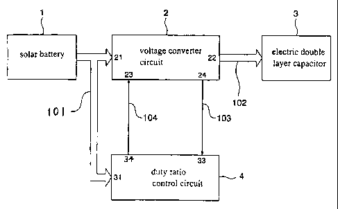
A solar power charging system includes a solar battery 1, a
voltage converter circuit 2, an electric double layer capacitor 3 and a duty
ratio control circuit 4. The solar battery 1 generates a generated voltage 101
upon receipt of incident light or sunshine. The solar battery 1 is
electrically
coupled to a power input terminal 21 of the voltage converter circuit 2 for
supplying the generated voltage 101 to the voltage converter circuit 2. The
solar battery 1 is electrically coupled to a power input terminal 31 of the
duty ratio control circuit 4 for supplying the generated voltage 101 to the
duty ratio control circuit 4.
A current inputted into the voltage converter circuit 2 is much
larger than a current inputted into the duty ratio control circuit 4. A
majority of the generated power by the solar battery 1 is consumed by the
voltage converter circuit 2, whilst a remaining minority of the generated
power by the solar battery 1 is consumed by the duty ratio control circuit 4.
The voltage converter circuit 2 has a detected voltage output
terminal 24. The voltage converter circuit 2 receives the current from the
solar battery 1 and generates a detected voltage 103 based on the received
current, so that the detected voltage 103 is outputted from the detecting
voltage output terminal 24 of the voltage converter circuit 2. The detected
voltage output terminal 24 of the voltage converter circuit 2 is electrically
coupled to a detected voltage input terminal 33 of the duty ratio control
circuit 4, so that the detected voltage 103 is inputted through the detected
voltage input terminal 33 into the duty ratio control circuit 4.
Page 7
CA 02366352 2002-O1-24
Pf-2915/nec/canada/mh
The voltage converter circuit 2 has a driving clock input terminal
23. The duty ratio control circuit 4 has a driving clock output terminal 34
which is electrically coupled to the driving clock input terminal 23. The
duty ratio control circuit 4 controls a duty ratio of a driving clock and
generates a driving clock 104 with the controlled duty ratio based on the
generated voltage 101 and the detected voltage 103. The driving clock 104
with the controlled duty ratio is outputted from the driving clock output
terminal 34 and then inputted through the driving clock input terminal 23
into the voltage converter circuit 2. The voltage converter circuit 2
operates,
in synchronizing with the driving clock 104, to convert the generated
voltage 101 into a charge voltage 102. The voltage converter circuit 2 has a
charge voltage output terminal 22, so that the charge voltage 102 is
outputted from the charge voltage output terminal 22. This charge voltage
102 output terminal 22 of the voltage converter circuit 2 is electrically
coupled to the electric double layer capacitor 3, so that the charge voltage
102 is supplied to the electric double layer capacitor 3, whereby the electric
double layer capacitor 3 is charged by the charge voltage 102.
The electric double layer capacitor 3 stores a power supplied
through the voltage converter circuit 2 from the solar battery 1. The electric
double layer capacitor 3 is longer in life-time of charge/discharge times
than a chemical secondary battery.
FIG. 3 is a circuit diagram illustrative of an internal circuit
configuration of the voltage converter circuit included in the solar power
charging system shown in FIG. 2. The voltage converter circuit 2 may
Page 8
CA 02366352 2002-O1-24
Pf-2915/nec/canada/mh
comprise a DC chopper circuit of boosting type as shown in FIG. 3. The
voltage converter circuit 2 has capacitors C1 and C2, an inductor L1, a
diode D1, an n-channel transistor Qnl, and a resistance R1. The voltage
converter circuit 2 also has the power input terminal 21, the charge voltage
output terminal 22, the driving clock input terminal 23, and the detected
voltage output terminal 24.
The power input terminal 21 is connected through the capacitor
C1 to a ground. The power input terminal 21 is connected through the
inductor L1 to a node Na. The node Na is connected through the n-channel
transistor Qnl to a node Nb. The node Nb is also connected through the
resistance R1 to the ground. The node Nb is connected directly to the
detected voltage output terminal 24, from which the detected voltage 103 is
outputted. A gate of the n-channel transistor Qn1 is connected directly to
the driving clock input terminal 23 for applying the driving clock 104 to the
gate of the n-channel transistor Qnl.
The node Na is also connected through the diode D1 to the
charge voltage output terminal 22. The charge voltage output terminal 22 is
connected through the capacitor C2 to the ground.
FIG. 4 is a timing chart illustrative of waveforms of driving clock
signal, voltage at the node Na, currents I1 and I3, and voltage Vc2 of the
voltage converter circuit of FIG. 3. The inductor L1 has a current I1 which
flows in a direction from the power input terminal 21 toward the node Na.
The n-channel transistor Qn1 has a current I2 which flows in a direction
from the node Na to the node Nb. The diode D1 has a current I3 which
Page 9
CA 02366352 2002-O1-24
Pf-2915/nec/canada/mh
flows a direction from the node Na to the charge voltage output terminal 22.
The capacitor C1 has a voltage Vcl. The capacitor C2 has a voltage Vc2.
The driving clock 104 has a cycle T1 which comprises an ON-
time period T2 and an OFF-time period T3. In the ON-time period T2, the
driving clock 104 is in high level "H". In the OFF-time period T3, the
driving clock 104 is in low level "L". The n-channel transistor Qn1 is
placed in ON-state during the ON-time period T2, because the driving
clock 104 is in high level "H". The n-channel transistor Qn1 is placed in
OFF-state during the OFF-time period T3, because the driving clock 104 is
in low level "L".
In the ON-time period T2 , the n-channel transistor Qn1 is placed
in ON-state, whereby the node Na has the ground potential, and the diode
D1 is biased in reverse direction, and the current I3 is zero. The capacitor
C2 is discharged to supply a charge current to the electric double layer
capacitor, whereby the voltage Vc2 of the capacitor C2 almost linearly
decreases from a high voltage level Ec to a low voltage level Eb.
Since the n-channel transistor Qn1 is placed in ON-state, then a
current flows through a closed circuit which comprises the inductor L1, the
n-channel transistor Qnl, and the resistance R1, wherein the current I1 is
equal to the current I2. The current I1 almost linearly increases from a low
current value Aa to a high current value Ab.
The node Nb has a potential Vb which is given by Vb = I2 X R1.
The node Nb has the same potential as the node Na. The detected voltage
103 is the potential of the node Nb, for which reason the detected voltage
Page 10
CA 02366352 2002-O1-24
Pf-2915/nec/canada/mh
103 has the voltage level equal to the potential of the node Na. The voltage
level of the detected voltage 103 almost linearly increases from 0 to the
high level Ea. The inductor L1 increases in an internal magnetic flux.
In the OFF-time period T3, the n-channel transistor Qn1 is placed
in the OFF-state, whereby the node Na and the node Nb are electrically
separated. The inductor Ll decreases in the internal magnetic flux,
whereby an induced electromotive force is caused by the inductor L1 to
suppress the decrease in the internal magnetic flux of the inductor L1. The
generated induced electromotive force and the voltage Vc1 of the capacitor
C1 are applied to the node Na, whereby the node Na has an increased
potential Vc2 which is higher than Vcl. The increased potential Vc2 of the
node Na applies a forward bias to the diode D1.
Since the n-channel transistor Qn1 is placed in OFF-state, then
another current flows through another closed circuit which comprises the
capacitor C1, the inductor L1, the diode D1 and the capacitor C2, wherein
the current I1 is equal to the current I3. The capacitor C2 is charged,
whereby the current I1 almost linearly decreases from the high current
value Ab to the low current value Aa.
FIG. 5 is a circuit diagram illustrative of an internal circuit
configuration of the duty ratio control circuit included in the solar power
charging system shown in FIG. 2. The duty ratio control circuit 4 has
resistances R2, R3, R4, R5, R6 and R7, an operational amplifier Opl, and a
reference voltage Vfl. The duty ratio control circuit 4 also has the power
input terminal 31, a control output terminal 32, the detected voltage input
Page 11
CA 02366352 2002-O1-24
Pf-2915/nec/canada/mh
terminal 33, and the driving clock output terminal 34.
The power input terminal 31 is connected through the resistance
R2 to a node Nc. The node Nc is connected through the resistance R3 to a
ground. The node Nc is connected through the resistance R4 to an inversion
input terminal of the operational amplifier Opl. A non-inversion input
terminal of the operational amplifier Opl is connected through the
reference voltage Vf1 to the ground. An output terminal of the operational
amplifier Op1 is connected to a node Nd. The node Nd is connected
through the resistance RS to the inversion input terminal of the operational
amplifier Opl. The node Nd is connected through the resistance R6 to a
node Ne. The node Ne is connected directly to the control output terminal
32. The node Ne is connected through the resistance R7 to the detected
voltage input terminal 33. The control output terminal 32 is connected
through the resistance R7 to the detected voltage input terminal 33.
The duty ratio control circuit 4 has a driving clock generator
circuit which is not shown in FIG. 5, wherein the driving clock generator
circuit is connected to the control output terminal 32. A clock control
voltage 105 is supplied through the control output terminal 32 to the
driving clock generator circuit.
The node Nc has a potential Vc given by
Vc = R3/(R2 + R3) Vi ------ (1)
where Vi is the voltage of the generated voltage 101 generated by the solar
battery 1.
The operational amplifier Op1 performs an inversion
Page 12
CA 02366352 2002-O1-24
Pf-2915/nec/canada/mh
amplification of the potential Vc by a potential difference from the
reference voltage Vfl.
The node Nd has a potential Vd given by
Vd = ~(R4 + RS)/R4} Vf1- (RS/R4) Vi ------ (2).
In the voltage converter circuit 2, the potential Vb of the node Nb
is generated in proportion to the current I2 flowing through the n-channel
transistor Qnl. The potential Vb is supplied as the detected voltage 103
from the detected voltage output terminal 24 to the detected voltage input
terminal 33 of the duty ratio control circuit 4, whereby the potential Ve is
generated at the node Ne.
Ve = (Vb - Vd)x R6 /(R6 + R7) ------ (3).
The duty ratio control circuit 4 supplies the potential Ve as the
clock control voltage 105 to the driving clock generator circuit, so that the
driving clock generator circuit controls the duty ratio based on the clock
control voltage 105 to generate the driving clock 104.
The driving clock generator recognizes the current I1 based on
the clock control voltage 105 with the potential Ve. The upper limit Ab and
the lower limit Aa have previously been set so that an averaged value of the
current I1 corresponds to an input current such that the solar battery
provides the maximum charge power to obtain the maximum output. The
driving clock generator circuit controls the duty ratio of the driving clock
104 based on the variation of he current I1.
The driving clock 104 is set high level, and the driving clock
generator circuit monitors the current I1. If the current I1 exceeds the upper
Page 13
CA 02366352 2002-O1-24
Pf 2915/nec/canada/mh
limit Ab, then the driving clock generator circuit sets the driver clock 104
at the low level, whereby the driving clock generator circuit counts a time.
If the time passes a predetermined value, then the driving clock generator
circuit sets the driver clock 104 at the high level.
The duty ratio control circuit 4 recognizes, based on the
generated voltage 101 and the detected voltage 103, a power consumed by
the voltage converter circuit 2 to generate a clock control voltage 105 with
a controlled duty ratio.
FIG. 6 is a diagram illustrative of a voltage-current characteristic
curve of the solar battery. The voltage-current characteristic is measured
based on four illuminances, S1, S2, S3 and S4. The solar battery shows
respective maximum powers W1, W2, W3 and W4, at the four
illuminances S1, S2, S3 and S4. The illuminance is largely variable
depending on the sunshine condition. The maximum power of the solar
battery largely depends on the illuminance.
FIG. 7 is a diagram illustrative of variation in power under
maximum power conditions over the illuminance. A real line represents the
characteristic curve of the power under maximum power conditions. A
broken line represents a preset approximate linear line in accordance with
the characteristic curve at the maximum power. The characteristic curve of
the maximum output is given by the four points of the maximum output
powers W1, W2, W3 and W4. The approximate line is obtained by
assuming that the voltage and the current have a proportional relationship
under the maximum output conditions.
Page 14
CA 02366352 2002-O1-24
Pf-2915/nec/canada/mh
As described above, the duty ratio control circuit 4 has the
driving clock generator circuit which is not shown. The clock control
voltage is inputted through an input terminal into the driving clock
generator circuit of the duty ratio control circuit 4. The solar battery 1
supplies the maximum output power to a load when the current of the
maximum output flows through the load upon application of the generated
voltage 101. The current of the maximum output represents a crossing
point to the generated voltage 101 on the characteristic curve of the
maximum output.
The driving clock generator circuit of the duty ratio control
circuit 4 controls the ON-time period T2 of the driving clock 104 based on
the potential Ve of the clock control voltage 105. The voltage converter
circuit 2 consumes the current I1 which comprises the current I2 and the
current I3.
The majority of the power supplied from the solar battery 1 is
consumed by the voltage converter circuit 2. The duty ratio control circuit 4
controls the voltage converter circuit 2 so that the consumed power moves
on the approximate linear line.
In accordance with the embodiment, the duty ratio of the driving
clock is controlled based on the maximum charge power which is decided
by the generated voltage, whereby the capacitor can be charged at the
maximum output of the solar battery, wherein the maximum output may
vary depending on the sunshine conditions.
Page 15
CA 02366352 2002-O1-24
Pf-2915/nec/canada/mh
SFC'OND EMBODIMENT
A second embodiment according to the present invention will be
described in detail with reference to the drawings. FIG. $ is a circuit
diagram illustrative of an internal circuit configuration of other voltage
converter circuit included in the solar power charging system in a second
embodiment in accordance with the present invention. The second
embodiment is different from the first embodiment only in the circuit
configuration of the voltage converter circuit.
The voltage converter circuit 2A may comprise a DC chopper
circuit of boosting-up-and-down type. The voltage converter circuit 2A has
capacitors C1, C2 and C3, inductors L1 and L2, a diode D1, an n-channel
transistor Qnl, and a resistance R1. The voltage converter circuit 2A also
has the power input terminal 21, the charge voltage output terminal 22, the
driving clock input terminal 23, and the detected voltage output terminal
24.
The power input terminal 21 is connected through the capacitor
C1 to a ground. The power input terminal 21 is connected through the
inductor Ll to a node Na. The node Na is connected through the n-channel
transistor Qn1 to a node Nb. The node Nb is also connected through the
resistance R1 to the ground. The node Nb is connected directly to the
detected voltage output terminal 24, from which the detected voltage 103 is
outputted. A gate of the n-channel transistor Qn1 is connected directly to
the driving clock input terminal 23 for applying the driving clock 104 to the
gate of the n-channel transistor Qnl.
Page 16
CA 02366352 2002-O1-24
Pf-2915/nec/canada/mh
The node Na is also connected through the capacitor C3 to a
node Nc. The node Nc is connected through the inductor L2 to the ground.
The node Nc is also connected through the diode D1 to the charge voltage
output terminal 22. The charge voltage output terminal 22 is connected
through the capacitor C2 to the ground.
The voltage converter circuit 2A adjusts the generated voltage
101 with rising or falling the voltage level to generate the charge voltage
102. Since the voltage converter circuit 2A is capable of both rising and
falling the voltage level of the generated voltage 101, this increases
acceptable ranges of the generated voltage 101 and the charge voltage 102,
whereby the conditions for selecting the solar battery 1 and the electric
double layer capacitor 3.
In accordance with the embodiment, the duty ratio of the driving
clock is controlled based on the maximum charge power which is decided
by the generated voltage, whereby the capacitor can be charged at the
maximum output of the solar battery, wherein the maximum output may
vary depending on the sunshine conditions.
It is possible as a modification to the foregoing embodiments that
a microcomputer is integrated into the duty ratio control circuit 4 for
changing the circuit type of the voltage converter circuit, whereby the input
current at the maximum output from the generated voltage 101 can be
found under the control of the microcomputer.
Although the invention has been described above in connection
with several preferred embodiments therefor, it will be appreciated that
Page 17
CA 02366352 2002-O1-24
Pf-2915/nec/canada/mh
those embodiments have been provided solely for illustrating the invention,
and not in a limiting sense. Numerous modifications and substitutions of
equivalent materials and techniques will be readily apparent to those skilled
in the art after reading the present application, and all such modifications
and substitutions are expressly understood to fall within the true scope and
spirit of the appended claims.
Page 18