Note: Descriptions are shown in the official language in which they were submitted.
CA 02366898 2001-08-24
WO 00/54163 PCT/GB00/00754 _
ELASTIC INTERFACE APPARATUS AND METHOD THEREFOR
TECHNICAL FIELD
The present invention relates in general to data processing systems,
and in particular, to the interface between dynamic, or clocked,
integrated circuit chips in a data processing system.
BACKGROUND INFORMATION
Modern data processing systems require the transfer of data between
dynamic, or clocked, circuits embodied in multiple chips in the system.
For example, data may need to be transferred between central processing
units (CPUs) in a multi-CPU system, or between a CPU and the memory system
which may include a memory controller and off-chip cache. Data transfers
are synchronous, and data is expected to be delivered to the circuitry on
the chip on a predetermined system cycle . As CPU speeds have increased,
the speed of the interface between chips (bus cycle time) has become the
limiting constraint as the latency across the interface exceeds the system
clock period. In order to maintain system synchronisation, the system
designer must slow the speed of the bus in order that the cycle on which
data arrives be unambiguous.
This may be further understood by referring to FIGURE lA, in which
is depicted, in block diagram form, a prior art interface between two
integrated circuit chips, chip 102 and chip 104 in a data processing
system. Each of chips 102 and 104 receive a reference clock 106 coupled
to a phase lock loop, PLL 108. PLL 108 generates a local clock, clock 110
in chip 102 and clock 111 in chip 104, locked to reference clock 106.
Reference clock 106 provides a "time zero" reference, and may be asserted
for multiple periods of local clocks 110 and 111, depending on the
multiplication of PLL 108. The bus clock 113 is derived from reference
clock 106 by dividing local clock 110 by a predetermined integer, N, in
divider 112. Data to be sent from chip 102 to chip 104 is latched on a
predetermined edge of the divided local clock 111 and driven on to data
line 116 via driver 18. Data is received at receiver (RX) 120 and
captured into destination latch 122 on a predetermined edge of the divided
local clock 110 in chip 104. Due to the physical separation of chip 102
and chip 104, the data appears at input 124 of destination latch 122
delayed in time. (The contribution of RX 120 to the latency is typically
CA 02366898 2001-08-24
WO 00/54163 PCT/GB00/00754
2
small relative to the delay due to the data transfer.) The time delay is
referred to as the latency, and will be discussed further in conjunction
with FIGURE 1B.
Similarly, chip 104 sends data to chip 102 via data line 126. Data
to be sent from chip 104 is latched in latch 128 on a predetermined edge
of the output signal from divider 130 which divides local clock 111 by N.
The data is driven onto data line 126 via driver 132 and captured on
destination latch 134 via receiver 136. The data input to chip 102 is
captured into data latch 134 on a predetermined edge of an output of
divider 130 which also divides local clock 110 by N.
In FIGURE 1B, there is illustrated an exemplary timing diagram for
interface 100 of FIGURE lA, in accordance with the prior art. Data 115
sent from chip 102 to chip 104 is latched, in latch 114, on a rising edge,
t,, of bus clock 113. Bus clock 113 is generated by dividing local clock
110 by N in dividers 112 and 130 in chip 102. Following a delay by the
latency, TI, data 117 appears at an input to destination latch 122, and is
latched on rising edge t2 of bus clock 123. Bus clock 123 is generated by
dividing local clock 111 by N in dividers 112 and 130 in chip 104. Thus,
in the prior art in accordance with FIGURE 1B, data 125 appears in chip
104 one bus cycle following its launch from chip 102. In FIGURE 1B, there
is zero skew between bus clock 113 and bus clock 123.
If, in interface 1.00 in FIGURE lA, the bus clock speed is
increased, the latency may exceed one bus clock cycle. Then the exemplary
timing diagram illustrated in FIGURE 1C_ may result. As before, data 115
has been latched on edge t, of bus clock 113. Data 117 appears at input
124 of destination latch 122 after latency time, T1 which is longer than
the period of bus clock 113 and bus clock 123. Data 117 is latched on
edge C, of bus clock 123 in chip 104 to provide data 125 on chip 104. If
interface 100 between chips 102 and 104 represents the interface having
the longest latency from among a plurality of interfaces between chip 102
and the plurality of other chips within a data processing system, then the
two cycle latency illustrated in FIGURE 1C represents the "target" cycle
for the transmission and capture of data between chips, such as chip 102
and chip 104. The target cycle is the predetermined cycle at which data
is expected by the chip. Interfaces having a shorter latency may need to
be padded, in accordance with the prior art, in order to ensure
synchronous operation. The padding ensures that faster paths in interface
CA 02366898 2001-08-24
WO 00/54163 PCT/GB00/00754
3
100 have latencies greater than one bus clock cycle and less than two bus
clock cycles, whereby data synchronisation may be maintained.
This may be further understood by referring now to FIGURE 1D,
illustrating a plurality 101 of chips, chips 102, 103 and 104. Chip 102
and chip 104 are coupled on "slow" path 152 having a long latency, TS.
Chip 103 is coupled to chip 102 via "fast" path 154 having a short latency
period, TP. A "nominal" path coupling plurality 101 of chips 102-105 has
latency TM, such as the latency on path 156 between chip 102 and chip 105.
The timing diagram in FIGURE lE provides further detail. FIGURE lE
illustrates a timing diagram similar to that in FIGURE 1C in which the
target cycle for the capture of data into a receiving chip is two bus
cycles. In FIGURE lE, the nominal latency, TM, is shown to be 1.5 bus
cycles, the fast path latency, TF, is illustrated to be just greater than
one bus cycle, and the slow path latency, TS, is shown to be slightly less
than two bus cycles. In this case, each of the plurality of chips 101 in
FIGURE 1D capture data on the target cycle, two bus cycles after data
launch.
If, however, the fast path is shorter, illustrated by fast path
latency data synchronisation is lost. In this case, data arrives at chip
103 prior to transition t2 of the chip 103 bus clock as illustrated by the
dotted portion of data 117 at chip 103, and is latched into chip 103 after
one bus cycle. This is illustrated by the dotted portion of data 125 in
chip 103. In order to restore synchronisation, the fast path, path 154,
between chips 102 and 103 would require padding to increase the fast path
latency, from to TF. Consequently, the timing of such a prior art
interface is tuned to a specific operating range, a particular interface
length, and is valid only for the technology for which the design was
timed and analysed.
Likewise, increasing the clock speed of the chips in FIGURE 1D will
result in a loss of synchronisation. This may be understood by
considering an explicit example. The local clock cycle time is first
taken have a 1 nanosecond (ns) period. The bus clock will have a period
that is a fixed multiple, which will be taken to be two, of the local
clock. Let the nominal latency of the interface, TM, be ins with +/-.99 ns
of timing variation, i . a . the best case or fast path, TF, is 2ns and the
worse case, or slow path, TS, is 4ns. The data will arrive after two ns and
CA 02366898 2001-08-24
WO 00/54163 PCT/GB00/00754
4
before four ns. Hence the interface will operate under all conditions i.e.
data is guaranteed to arrive after the first bus cycle and before the
second bus cycle. However if the speed of the chips is increased to a
.9ns cycle time, the bus cycle time is changed to l.8ns. In order to
ensure enough time for the data to propagate across the interface under
worse case conditions the data must not be captured before 2.5 bus cycles,
or 4.Sns, because two bus cycles is less than the slow path time, TS, or
4ns. Then, in order to operate a l.8ns bus cycle, the fastest data can
arrive is 1.5*1.8= 2.7ns (one bus cycle earlier), to ensure data arrives
on the same cycle for all conditions. However, the earliest data can
arrive from the above latency numbers is via the fast path with a TF of
ins-.99ns=2.Olns. Thus, operating at a bus cycle time of l.8ns cannot be
supported in a conventional synchronous design. In order to operate
synchronously, the bus to processor ratio must be slowed to at least 3:1
and operate at a 2.7ns cycle time (2.7ns*1.5 cycles =4.05ns and 2.7nS*.5
cycles =1.35ns) which militates against the increase in local clock speed.
Thus, there is a need in the art for apparatus and methods to
accommodate data transfers between chips in a data processing system
having increasing clock speeds. In particular, there is a need for
methods and apparatus to ensure data synchronisation between chips in data
processing systems in which path latencies vary over more than one bus
cycle, and in which the need for design specific hardware padding is
eliminated.
30
It is an object of the present invention to provide a technique
which overcomes the above drawbacks.
SiJNIMARY OF THE INVENTION
According to the present invention we provide an interface apparatus
comprising:
a first storage device operable for storing a first set of data
values;
a second storage device operable for storing a second set of data
values; and
circuitry coupled to said first and second storage devices operable
for sequentially outputting a first data value from said first storage
device and a second data value from said second storage device in response
to at least one control signal, wherein said first and second storage
CA 02366898 2001-08-24
WO 00/54163 PCT/GB00/00754
devices hold data values for a predetermined number of cycles of a first
clock.
Also according to the present invention we provide a method of
5 interfacing integrated circuit devices comprising the steps of:
storing a first set of data values in a first storage element,
wherein each data value of said first set is stored for a predetermined
number of cycles of a first clock;
storing a second set of data values in a second set of storage
l0 elements wherein each data value of said second set is stored for a
predetermined number of cycles of a first clock; and
sequentially outputting a first data value from said first storage
device and a second data value from said second storage device in response
to at least one control signal.
The foregoing has outlined rather broadly the features and technical
advantages of the present invention in order that the detailed description
of the invention that follows may be better understood. Additional
features and advantages of the invention will be described hereinafter
which form the subject of the claims of the invention.
BRIEF DESCRIPTION OF THE DRAWINGS
For a more complete understanding of the present invention, and the
advantages thereof, reference is now made to the following descriptions
taken in conjunction with the accompanying drawings, in which:
FIGURE lA illustrates a chip interface in accordance with the prior
art ;
FIGURE 1B schematically illustrates a timing diagram for an
embodiment of the chip interface of FIGURE lA, in accordance with the
prior art;
FIGURE 1C illustrates a timing diagram for another embodiment of the
chip interface of FIGURE lA, according to the prior art;
FIGURE 1D illustrates a plurality of interconnected chips in a data
processing system;
CA 02366898 2001-08-24
WO 00/54163 PCT/GB00/00754
6
FIGURE lE schematically illustrates a timing diagram for an
embodiment of the plurality of interconnected chips of FIGURE D;
FIGURE 2 illustrates, in block diagram form, a representative
hardware environment for practising the invention;
FIGURE 3 illustrates, in block diagram form, a chip interface in
accordance with an embodiment of the present invention;
FIGURE 4A illustrates, in block diagram form, an elastic interface
in accordance with an embodiment of the present invention;
FIGURE 4B schematically illustrates a timing diagram of the
embodiment of the present invention of FIGURE 3A;
FIGURE 5 illustrates an alternative embodiment of a chip interface
in accordance with the present invention;
FIGURE 6A illustrates another alternative embodiment of an elastic
interface according to the present invention;
FIGURE 6B schematically illustrates a timing diagram of the elastic
interface of FIGURE 5A;
FIGURE 7A illustrates. another alternative embodiment of an elastic
embodiment according to the present invention;
FIGURE 7B schematically illustrates a timing diagram for the
embodiment of FIGURE 7A;
FIGURE 8A illustrates in block diagram form yet another alternative
embodiment of the elastic interface according to the present invention;
and
FIGURE 8B schematically illustrates a timing diagram for the
embodiment of FIGURE 8A.
CA 02366898 2001-08-24
WO 00/54163 PCT/GB00/00754
DETAILED DESCRIPTION
The present invention provides an elastic interface mechanism that
implements data synchronisation among a plurality of data processing chips
in a data processing system. Data synchronisation is accomplished without
the need for padding which otherwise complicates the physical wiring, and
adds complexity to the hardware design. The "elasticity" of the interface
accounts for the physical difference between paths coupling the data
processing chips in the system. By capturing the received data into a
plurality of storage elements, and selectively steering the latched data,
data synchronisation is provided in a data processing system having
latencies that vary by more than one bus clock cycle. Synchronisation may
be established dynamically by performing an initialisation alignment
procedure, on power-up or following a reset. In this way, synchronisation
of data may be accomplished in accordance with the principles of the
present invention without the need for a timing analysis of the board
design and fast path padding.
In the following description, numerous specific details are set
forth such as bus clock frequencies and synchronisation cycles, clock
edges, etc. to provide a thorough understanding of the present invention.
However, it will be obvious to those skilled in the art that the present
invention may be practised without such specific details. In other
instances, well-known circuits have been shown in block diagram form in
order not to obscure the present invention in unnecessary detail.
Refer now to FIGURES 2-9 wherein depicted elements are not
necessarily shown to scale and wherein like or similar elements are
designated by the same reference numeral through the several views.
A representative hardware environment for practising the present
invention is depicted in FIGURE 2, which illustrates a typical hardware
configuration cf data processing system 213 in accordance with the subject
invention having central processing unit (CPU) 210, such as a conventional
microprocessor, and a number of other units interconnected via system bus
212. Data processing system 213 includes random access memory (RAM) 214,
read only memory (ROM) 216, and input/output (I/O) adapter 218 for
connecting peripheral devices such as disk units 220 and tape drives 240
to bus 212, user interface adapter 222 for connecting keyboard 224, mouse
226, and/or other user interface devices such as a touch screen device
CA 02366898 2001-08-24
WO 00/54163 PCT/GB00/00754
8
(not shown) to bus 212, communication adapter 234 for connecting
workstation 213 to a data processing network, and display adapter 236 for
connecting bus 212 to display device 238. CPU 210 may include other
circuitry not shown herein, which will include circuitry commonly found
within a microprocessor, e.g., execution unit, bus interface unit,
arithmetic logic unit, etc. The interface of the present invention may be
included in CPU 210. Additionally, the present invention may be
incorporated into storage devices, such as RAM 214 (which may include
memory control circuitry, not shown herein). CPU 210 may also reside on a
single integrated circuit.
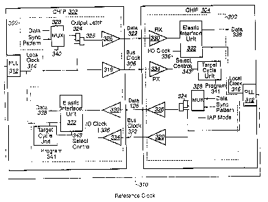
Refer now to FIGURE 3 in which is illustrated an interface 300 in
accordance with the present invention. Interface 300 is incorporated in
each of chip 302 and chip 304 which communicate data with each other via a
respective interface 300. (Although the embodiment of the present
invention is described in the context of a chip to chip interface, the
principals of the present invention may be embodied in an interface
between any pair of clocked latches.) Data is transferred between chips
302 and 304 at a rate determined by a bus clock, bus clocks 306 and 308.
Bus clocks 306 and 308 are nominally the same frequency, and are derived
from reference clock 310 provided to a PLL, PLL 312 in each of chips 302
and 304. In an embodiment of the present invention, reference clock 310
may be a system clock. Each of PLL 312 outputs a local clock, local clock
314 in chip 302 and local clock 316 in chip 304 which is locked in phase
to reference clock 310 , and . may be a preselected integer, M, multiple of
the period of reference clock 310. Local clock 314 is buffered by driver
318 to provide bus clock 306 from chip 302. Similarly, local clock 316 is
buffered by driver 320 to provide bus clock 308 from chip 304.
The bus clock is provided along with the data communicated from the
chip. Data 322 from chip 302 is latched into output latch 324 and driven
and buffered by driver 326. The data is latched on a preselected edge of
local clock 314. The data is received via multiplexer (I~IUX) 328. MUX 328
also receives a predetermined synchronisation pattern in conjunction with
the alignment procedure. These will be further described below.
Data 322 is buffered by receiver (RX) 330 and provided to an elastic
interface unit 332. Bus clock 306 sent along with data 322 is buffered by
RX 334, the output of which forms I/O clock 336, also provided to elastic
interface 332. Data from chip 304 being sent to chip 302, along with bus
CA 02366898 2004-10-21
clock 308, is similarly received by interface 300 in chip 302, and it would be
understood that the
description of elastic device 332 to follow applies equally well in the
receipt of data by chip 302
from chip 304.
Target cycle unit 339 sets the target cycle on which data is latched by the
local clock in the
receiving chip, such as local clock 316 in chip 304. The target cycle
discussed in detail in
conjunction with FIGURES 4A/B, illustrating an interface 322 having an
elasticity of two. For an
interface having an elasticity, E, target cycle unit may include a divide-by-E
circuit. Additionally,
target cycle unit 339 may include a programming register for holding the
predetermined target cycle
value, which may be loaded via target program 341. The target cycle programmed
in target cycle
unit 339 in chip 302 may be different than the target cycle programmed in
target cycle unit 339 in
chip 304. Target cycle unit 339 outputs select control 343, which may include
a plurality of signals,
depending on the embodiment of interface unit 332 and the corresponding
elasticity, E. Select
control 343 will be further described in conjunction with FIGURES 4A-8B in
which embodiments
of interface unit 332 are illustrated.
Refer now to FIGURE 4A illustrating an embodiment of an elastic interface unit
332 in
accordance with the present invention. Unit 332 includes MUX 402 having an
input 404 which
receives data from RX 330. Output 406 of MUX 402 is coupled to the data (D)
input of latch 408.
Latch 408 is clocked by I/O clock 336. Latch 408 latches data at the D input
thereof on a rising edge
of clock 436 and holds the data until a next rising edge of clock 336. Output
410 of latch 408 is
coupled back to a second input, input 412 of MUX 402. MUX 402 selects between
input 404 and
input 412 for outputting on output 406 in response to gate 414.
Gate 414 is derived from bus clock 306 and has twice the period of bus clock
306. Gate 414
may be generated using a delay lock loop (DLL). The phase of gate 414 is set
during the
initialization alignment procedure discussed below, and the operation of gate
414 will be further
described in conjunction with FIGURE 4B.
AUS9-1998-0208 9
CA 02366898 2001-08-24
WO 00/54163 PCT/GB00/00754
The data from RX 330 is also fed in parallel to a second MUX, MUX
416, on input 418. Output 420 of MUX 416 is coupled to a D input of a
second latch, latch 422, which is also clocked by I/O clock 336, and
latches data on a rising edge of I/O clock 336 and holds the data until a
5 subsequent rising edge of the clock. Output 424 of latch 422 is coupled
to a second input, input 426 of MUX 416.
MUX 416 selects between input 418 and input 426 in response to the
complement of gate 414, \gate 428. Thus, when one of MUXs 402 and 416 is
10 selecting for the data received from RX 330, the other is selecting for
the data held in its corresponding latch, one of latches 408 and 422. In
this way, a data bit previously stored in one of latches 408 and 422 is
held for an additional cycle of I/O clock 336.
Hence, two data streams are created, each of which is valid for two
periods of I/O clock 336. Because of the phase reversal between gate 414
and \gate 428, the two data streams are offset from each other by a
temporal width of one data value, that is, one cycle of I/O clock 336.
This may be further understood by referring to FIGURE 4B
illustrating a timing diagram in accordance with elastic interface unit
332 in FIGURE 4A. As previously described, data 325 held in output latch
324 is launched in synchrony with local clock 314 in chip 202. The data,
data 322, is received at RX 230 in chip 204, is delayed by the latency
represented by the path .between chips 202 and 204, as discussed
hereinabove in conjunction with FIGURE 1D. On rising edge tl of I/O clock
336, data value "a" of data 322 is captured by latch 408 via output 406 of
MUX 402. Because gate 414 is asserted, or "open", the data from RX 330 at
input 404 is thereby selected for outputting by MUX 402. (A gate will be
termed open when the corresponding MUX selects for the input receiving the
incoming data stream. Although this is associated with a "high" logic
state in the embodiment of FIGURE 4, it would be understood that an
alternative embodiment in which an open gate corresponded to a "low" logic
level would be within the spirit and scope of the present invention.)
Conversely, \gate 428 is negated. In response, MUX 416 selects a
previous data value held in latch 422, which is coupled back to the D
input of latch 422 through MUX 416. Thus, the data value held in latch
422 is retained for one additional period of I/O clock 336 which provides
CA 02366898 2004-10-21
the clock signal for both latch 408 and 322, as described in conjunction with
FIGURE 4A.
I/O clock 336 is obtained from bus clock 306, as shown in FIGURE 3. It is
assumed that,
at launch, bus clock 306 is centered in a data valid window, as illustrated in
FIGURE 4B. Bus
clock 306 suffers a delay across the interface just as the data does. The
latency is bus clock 306 at
chip 304 may be comparable to T, and this is reflected in I/O clock 336 which
is thereby centered
relative to data 322.
Gate 414 is generated such that the edges of gate 414 are phase coherent with
the falling
edges of I/O clock 336. At edge tZ of I/O clock 336, gate 414 falls, edge t3.
In response, MUX 402
selects for the output 410 of latch 408, coupled to input 412 of MUX 402, for
outputting at
output 406. As gate 414 is negated, \gate 428 is asserted, whereby MUX 416
selects for outputting
on output 420 the data from RX 330 on input 418. This is coupled to the D
input of latch 422. The
data received from RX 330 now corresponds to data value "b" of data 322.
At edge t4 of I/O clock 336, latches 408 and 422 latch the data at their
respective D inputs.
In latch 408, this corresponds to the previously held data value, value a of
data 322, which is then
held for an additional period of local clock 416. Latch 422 latches data value
b on its D input via
MUX 416 onto output 424.
At the next transition of I/O clock 336, t~, data value "c" is captured.
Because, at edge t~
gate 414 is asserted, data value c at data 322 appears on output 406 of MUX
402. Data value b is
retained in latch 422 because \gate 428 is negated, being the complement of
gate 414. As a stream
of data continues to arrive on data 322, elastic device 332 continues, in this
way, to generate two data
streams at outputs 410 and 424 of latches 408 and 422, respectively. The two
data streams contain
alternating portions of the input data stream arriving on data 422 which are
valid for two periods of
local clock 416, as illustrated in FIGURE 4B.
The structure of the input data stream is restored by alternately selecting
values from one of
the two data streams in synchrony with local
AUS9-1998-0208 11
CA 02366898 2001-08-24
WO 00/54163 PCT/GB00/00754
12
clock 416. A local clock target cycle is selected. The local clock
target cycle is the cycle at which data is to be captured into a
destination latch by the local clock, such as local clock 316 in FIGURES 3
and 4. The target cycle is determined by analysis. The target cycle must
be later in time than the worst case latency across the interface. For
example, in the embodiment depicted in FIGURE 4B, the target cycle has
been set to be three periods of local clock 316, corresponding to edge te.
The target cycle is measured from the zero time reference determined by
reference clock 310, as previously described in conjunction with reference
clock 106 in FIGURE lA. In the elasticity-two embodiment of FIGURE 4A/B,
the data arrival may be as much as two local clock cycles earlier than the
target cycle. In such an embodiment, target cycle unit 339 in FIGURE 3
includes a divide-by-two circuit.
With the target cycle set, data is selected for capture into
destination latch 430, in response to local clock 316, via MUX 432. MUX
432 has a pair of inputs, 434 and 436. Input 434 is coupled to output 410
of latch 408, and input 436 is coupled to output 424 of latch 422. MUX
422 selects for outputting one of the two data streams represented by the
output of latches 408 and 422 in response to select control 343. When
select control 343 has a first logic state, "high" in the embodiment of
FIGURE 4B, MUX 432 provides the data at input 434 to the D input of latch
430, and when select control 343 has a second predetermined logic state,
"low" in the embodiment of FIGURE 4B, data at input 436 of MUX 432 is
provided to the D input of -latch 430. Select control 343 has a period
that is twice the period of local clock 316, and is phase synchronous with
local clock 316 such that select control 343 has the first logic state,
and centred on, the target cycle. Thus, in FIGURE 4B, at edge t8 of local
clock 316, data value a at output 410 is coupled, via MUX 432, to the D
input of latch 430, and is latched by edge to of local clock 316. At the
next positive edge of local clock 316, t9, the next portion of the
transmitted data stream is latched into destination latch 430. Select
control 343 has advanced in phase by one-half period and, therefore, has
the second logic state, whereby output 424 of latch 422 is coupled to the
D input of latch 432 via MUX 432. At edge t5, data value b, at output 424
of latch 422 is latched into latch 432, and data value b appears on data
out 338. In subsequent cycles of local clock 316, elastic interface 332
restores data stream 225 by alternately selecting between output 410 of
latch 408 and output 424 of latch 422.
CA 02366898 2001-08-24
WO 00/54163 PCT/GB00/00754
13
Before data can be transmitted across elastic interface 322, gate
414 (and concomitantly the complement, \gate 428) must be initialised.
Because the latency across the interface can vary by more than one local
clock period, gate 414 must be initialised with the proper phase. As
previously described, the period of gate 414 is twice that of I/O clock
336, and local clock 316. Gate 414 is phase synchronous with I/O clock
316 such that flattop portions of gate 414 are centred on preselected
edges of I/O clock 336, the positive edges in the embodiment of FIGURE 4B.
Gate 414 may be initialised, in an embodiment of the present
invention, by transmitting a synchronisation (sync) pattern on power up or
reset. Referring again to FIGURE 3, in response to a reset or power up of
the data processing system, initialisation alignment procedure (IAP) mode
signal 340 is asserted, whereby MUX 328 selects for outputting a
predetermined sync pattern. IAP mode signal 340 may be asserted, in an
embodiment of the present invention, by CPU 210 in response to BIOS
instructions included in ROM 216.
In the embodiment of elastic interface unit 332 illustrated in
FIGURE 4A, data can arrive in a two-cycle window without creating
synchronisation problems, as previously described. Elastic interface unit
332 in FIGURE 4A is referred to as having an elasticity of two. In the
IAP, the synchronisation pattern is required to be periodic with a period,
P, equal to or greater than the elasticity of the elastic device. Thus,
for the elastic interface unit 332 of FIGURE 4B, a suitable
synchronisation pattern would be a plurality of bits alternating between
"1" and "0" with an initial bit of "1". Embodiments of elastic interfaces
having elasticities other than two will be described below, and the
synchronisation pattern will be modified accordingly. For example, for an
elastic interface having an elasticity N (discussed in conjunction with
FIGURE 8A/B below), a suitable pattern would be an initial bit of "1"
followed by N-1 bits of "0", which pattern then repeats. Other bit
patterns may also be used. For example, bit patterns complementary to the
exemplary patterns hereinabove may alternatively be used
In setting the phase of gate 414, output 410 of latch 408 may be
sampled while the sync pattern is being sent. Gate 414 is initialised
with a preselected phase. If, for the sync pattern described hereinabove
for elastic interface unit 332 having elasticity two, a "1" is detected at
output 410, then gate 414, and concomitantly \gate 428, are properly
CA 02366898 2004-10-21
phased. Otherwise, the phase of gate 414, and correspondingly \gate 428,
should be shifted by
one-half of the period of I/O clock 336. As previously discussed, gate 414 may
be generated using
a DLL.
The operation of an elastic interface in accordance with the principles of the
present
invention, such as elastic interface 300, may be further understood by
referring now to FIGURE 5.
In FIGURE 5, chip 302 exchanges data with chip 304, as in FIGURE 3, and
additionally with
chip 306. Chip 302 includes two of interfaces 300, one of which couples chip
302 to chip 304 via
an interface 300 included in chip 304, and the second of which couples chip
302 to chip 306 which
also includes an interface 300 in accordance with an embodiment of the present
invention. Path 502,
coupling chips 302 and 304 may be a fast path, similar to path 154 in FIGURE 1
D having a latency
TF, and path 504 coupling chip 302 to chip 306 maybe a slow path, such as path
152 in FIGURE 1D
with a latency TS. In an interface in accordance with the prior art, if the
latency difference between
paths 502 and 504 exceeds a period of the bus clock, path 502 would require
padding in order to
maintain synchronization of the data, as previously described. However,
interfaces 300
incorporating elastic interface unit 332 accommodates the difference in the
latencies between
path 502 and 504. By setting the target cycle in each of elastic interfaces
332 in chips 304 and 306
to be the same cycle, as described hereinabove, data synchrony among chips
302, 304, and 306 is
maintained.
Alternative embodiments of the present invention may be implemented. An
alternative
embodiment of interface unit 332 having an elasticity of two is illustrated in
FIGURE 6A. The
embodiment of elastic interface 232 shown in FIGURE 6A includes MUXs 402 and
416 driving
latches 408 and 422 as in the embodiment of elastic interface 232 illustrated
in FIGURE 4A.
However, interface unit 332 of FIGURE 6A includes a second capture latch,
latch 628, clocked by
local clock 316, in addition to latch 630 which corresponds to latch 430 in
the embodiment shown
in FIGURE 4A. Additionally, the output MUX 632, corresponding to MUX 432 in
FIGURE 4A has
been moved downstream of the capture latches, in the embodiment of interface
unit 332 in
FIGURE 6A.
AUS9-1998-0208 14
CA 02366898 2001-08-24
WO 00/54163 PCT/GB00100754
This reduces the latency through the interface itself. The D inputs
of latches 628 and 630 are coupled to outputs 424 and 410 of latches 422
and 408, respectively. The data at the D inputs of latches 628 and 630
are clocked into the latches by local clock 316. Thus, data is captured
5 in the local clock 316 ahead of MUX 632. Data stream 322 is restored by
selecting for outputting one of the outputs 634 and 636 of latches 628 and
630 via MUX 632, under the control of select control 343. This is similar
to the action of output MUX 432 in the embodiment of FIGURE 4A, however,
select control 343 is shifted in phase by one-half period as compared to
10 select control 343 in FIGURE 4A. In the embodiment of interface 322 in
FIGURE 6A, the data is latched on a rising edge of local clock 316. It
would be understood, however, by an artisan of ordinary skill that
alternative embodiments may latch the data on a falling edge provided that
other control signals are appropriately adjusted in phase. For example,
15 in an embodiment in which latches 628 and 630 latch on the falling edge of
local clock 316, select control 343 would have its phase shifted by
one-half period.
The operation of the embodiment of interface unit 332 of FIGURE 6A
may be further understood by referring now to FIGURE 6B illustrating a
timing diagram therefor. Because MUXs 402 and 416, and latches 408 and
422, as well as I/O clock 336 and local clock 316 are common to the
embodiments of interface unit 332 in FIGURES 4A and 4B, the portion of the
timing diagram illustrated in FIGURE 6B related to those structures will
not be discussed again, in the interest of brevity.
Focusing on the portion of the timing diagram of FIGURE 6B
associated with latches 628 and 630, and MUX 632, data value a is latched
onto output 634 of latch 630 on edge tee of local clock 316. Similarly,
data value b is latched onto output 636 of latch 628 on edge t9 ~ of local
clock 316. In order that data appear on data output 338 at the target
cycle, the rising edge of select control 343 must be delayed until edge t9~
of local clock 316, which coincides with the target cycle. Thus, data
value a appears on data out 338 from MUX 632 at edge t,o of select control
343. Hence, select control 343 is phase synchronous with local clock 316,
having flattops centered between rising transitions of local clock 316.
Similarly, data value b appears on data output 338 on falling edge tll of
select control 343, and data stream 322 continues to be restoreed
thereafter on subjsequent transitions of select control 343.
CA 02366898 2001-08-24
WO 00/54163 PCT/GB00/00754
16
Additionally, embodiments of elastic interface 232 having other
predetermined elasticities may be implemented in accordance with the
present invention. These may include half-period elasticities. An
embodiment of the present invention having an elasticity of 1.5 periods is
illustrated in FIGURE 7A. Data 322 is coupled to the D inputs of latches
702 and 704. Latches 702 and 704 are "polarity hold", or "flush" latches.
Such latches may also be referred to as "transparent" latches. When the
clock (C) in latch 702 has a first predetermined logic state, or level,
data on the D input flushes through to output 706. On the transition of
the clock from the first state to a predetermined second logic state,
latch 702 latches the data on the D input and the data on output 706 is
held until the subsequent transition of the clock from the second state to
the first state. (In the embodiment of FIGURE 7, the first state
corresponds to a "low" logic level and the second state corresponds to a
"high" logic level, whereby the transition constitutes a rising edge.
However, an alternative embodiment having the complementary logic states
would be within the spirit and scope of the present invention.) Latch 704
flushes data on its D input through to output 708 when its clock, C, has
the second logic level. The data is latched on the transition from the
second logic level to the first logic level of the clock, and held until
the clock transitions from the second logic level to the first logic
level, which in the embodiment of FIGURE 7, is "low. " The flush through
property allows data to become available without having to wait until a
latch is clocked, thereby implementing a "low-latency-low-elasticity"
embodiment of interface unit.332.
In the embodiment of elastic interface 322 illustrated in FIGURE 7A,
latches 702 and 704 are clocked by I/O clock 726. Elastic interface 322
of FIGURE 7A is a double data rate (DDR) device in that data is latched
into one of latches 702 and 704 on each transition of I/O clock 726, and
the period of I/O clock 726 is twice that of the local clocks, local
clock 314 and local clock 316, and bus clock 306. Bus clock 306 is
centred in a data wir_dow that is two local clock periods in width.
The embodiment of elastic interface unit 332 is FIGURE 7A may be
further understood by referring to the corresponding timing diagram shown
in FIGURE 7B. When data value a arrives at elastic interface unit 332, it
flushes through to output 706 of latch 702 because I/O clock 716 is low,
at "flattop" 752. In other words, data value a appears on output 706 of
latch 702 prior to edge t, of I/O clock 716.
CA 02366898 2001-08-24
WO 00/54163 PCT/GB00/00754
17
Data portion a precedes transition tl by one-quarter period of I/O
clock 336 which corresponds to one-half period of local clock 316. I/O
clock 336 is derived from the bus clock and is shifted in phase relative
to the bus clock at launch by the latency of the path between the chips,
as previously described. Additionally, I/O clock 716 is given a
one-quarter period phase advance. At edge tl, data value a is latched
whereby it is held for one period of local clock 316.
Similarly, data value b flushes through to output 708 of latch 704
when it arrives at elastic interface unit 332 from RX 230 because I/O
clock 716 is high, at flattop 754. Data value b is then held on output
708 by negative edge t2 of I/O clock 716. Data value b is held for one
period of local clock 316. Thus, data values appear on outputs 706 and
708 of latches 702 and 704, respectively, for 1.5 local clock periods,
which is the elasticity of the embodiment of elastic interface 332 of
FIGURE 7A.
Data stream 332 is reconstructed at output 338 by latches 710 and
712, and MUX 714. The two data streams represented by outputs 706 and 708
are, respectively, latched into latches 710 and 712 by local clock 316.
Data is latched on a predetermined edge (positive in the embodiment of
FIGURE 7) of local clock 316 wherein the target cycle may be set to occur
anywhere within one and one-half cycles of elasticity of data value a,
previously described. Thus,. data value a, in accordance with the timing
diagram in FIGURE 7B, is latched into latch 710 on edge t, of local clock
316 and switched onto data 338 via MUX 714 in response to select control
343. Data is selected from latch 710 in response to select control 343
having a first predetermined value and selected from latch 712 when select
control 343 has a second predetermined value. The first value is "high"
and the second "low" in the embodiment of FIGURE 7, however, it would be
understood that other predetermined values are within the spirit and scope
of the present invention. At edge t. of local clock 3i6, data value b is
latched into latch 712, and switched onto data 338 in response to select
control 343 have the second value. Subsequent data values are then
sequentially output on output 338 by alternately selecting the output from
latches 710 and 712 via MUX 714, as i~_lustrated in FIGURE 7B.
Additionally, elastic interfaces in accordance with the principles
of the present invention are expandable, whereby elasticities may be
CA 02366898 2001-08-24
WO 00/54163 PCT/GB00/00754
is
increased by adding steering and storage elements. An embodiment of an
elastic interface having an elasticity of N-1 bus clock periods is
illustrated in FIGURE 8A. Interface unit 32 includes a plurality, N of
MUXs 802. A first input 704 in each MUX receives data stream 322 from RX
330. A second input 806 receives a signal output by a corresponding one
of latches 808-818. Each of latches 808-818 includes a latch pair. In
latches 808, 812 and 816, the latch pairs have an internal output of a
first one of the pair coupled to an internal input of a second one of the
pair, in master-slave fashion. Latches 808, 812 and 816 provide an output
820 from the slave portion to an input 806 of the corresponding MUX 802.
The slave portion of latches 808, 812 and 816 latch the data on the D
input on a rising edge of I/O clock 336. Latches 808, 812, and 816 have
their respective D inputs coupled to the output of a corresponding MUX
802. Latches 810, 814 and 818 couple output 822 from the first one of the
latch pair to input 806 of a corresponding MUX 802. The first one of the
latch pair is transparent and data on a first input 828 flushes through to
output 822 on a "flattop" of I/O clock 336. Input 828 in each of latches
810, 814 and 818 is coupled to a corresponding output 826 from the second
one of the latch pair. Additionally, an input 830 to the second one of
the pair is coupled to an output of the corresponding MUX 802. The second
one of the latch pair is also transparent, and flushes data through on a
flattop of I/O clock 336. The first and second one of the pairs forming
latches 810, 814 and 818 flush data through on flattops of I/O clock 336
having opposite polarity.
MUXs 802 select between the signals on inputs 804 and 806 in
response to a corresponding gate signal, gates 832-842. Gate signals
832-840 will be discussed further in conjunction a timing diagram
illustrated in FIGURE 8B.
Data is latched into the local clock via data latches 844 , each of
which receives an output signal from a corresponding one of latches
808-818. Data is latched into data latches 844 by local clock 316.
Output 824 of latches 808, 812 and 87.6 is provided to the D input of a
corresponding data latch 844. Outputs 824 are obtained from the master
portion of latches 808, 812 and 816, which is transparent, as previously
described. The remaining ones of data latches 844 receive on their D
inputs the signal from output 826 from the second one of the latch pairs
forming the corresponding one of latches 810, 814 and 818. This second
one of the latch pairs is also a transparent latch with data flushing
CA 02366898 2001-08-24
WO 00/54163 PCT/GB00/00754
19
through on a polarity of I/O clock 336 opposite to that on which data
flushes through in the first one of the latch pairs.
MUX 846 selects one of the signals held in data latches 844 for
outputting. An output of each of data latches 844 is coupled to a
corresponding input, one of inputs 848-858. The signal is output to the
chip, such as chip 302 or 304 on output 860 of MUX 846. MUX 846 selects
among input 848-858 via select control 343. Select control 343 includes
k-signals, wherein 2'' is equal to N.
An alternative embodiment, having an elasticity of N may be
implemented using the circuitry shown in FIGURE SA. By coupling the
respective D inputs of data latches 844 to outputs 820 of the
corresponding one of latches 808,812 and 816, and to outputs 826 of the
corresponding one of latches 810,814 and 818 (instead of outputs 824 and
822 as shown in FIGURE 8A), an elasticity of N is obtained. The circuitry
of interface unit 332 in FIGURE 8A is otherwise unchanged.
Refer now to FIGURE 8B illustrating a timing diagram for interface
unit 332 illustrated in FIGURE 8A. Data value a arrives in the data
stream on data 322 after the interface latency of T1, and in response to
the assertion of gate 832 provided to the corresponding one of MUXs 802 ,
represented by "flattop" 862, data value a is passed through the
corresponding MUX 802 to the D input of latch 808. On edge t, of I/O clock
336, latch 808 holds data value a which is coupled back on output 820 of
latch 808 to input 806 of the corresponding one of MUXs 802. At edge t2 of
gate 832, the corresponding MUX 802 selects for the signal on input 806,
which has the data value a. Gate 832 is negated for N-1 periods of bus
clock 306, whereby the data value a is maintained on the D input of latch
808 and, therefore, on output 824 of latch 808. The data value a is held
for an additional cycle of bus clock 306 by transition t3 of I/O clock 336,
after which the transition t4 of gate 832 switches the corresponding MUX
802 to select for the data stream on data 322, whereby at edge cs of I/O
clock 336 the (N + 2) nd data value in data 2 is latched into latch 808 on
edge t; of I/O clock 336. Data value a is captured into the data latch 844
receiving output 824 of latch 808 on edge tb of local clock 316, and
appears on output 848. Data value a is held on output 848 for N periods
of bus clock 306.
CA 02366898 2001-08-24
WO 00/54163 PCT/GB00/00754
A next data value in data 332, data value b is similarly held for N
periods of bus clock 306 in the data latch 844 coupled to latch 810. When
data value b arrives at unit 332, gate 834 is asserted, represented by
"flattop" 864, and selects for data 332 on input 804 of the corresponding
5 MUX 802. Data value b appears at input 830 of latch 810 and is latched by
edge t, of I/O clock 336, whereby data value b appears on output 826 of
latch 810. Output 826 of latch 810 is fed back to input 828 of latch 810.
Because I/O clock 336 is negated following edge t,, data value b on output
826 of latch 10 falls through to output 822 of latch 810, where it is
10 coupled back to input 806 of the corresponding MUX 802. At edge to of I/O
clock 336, data value b is held on output 822 of latch 810. At edge t9 of
gate 834, the corresponding MUX 802 switches and selects input 806 for
outputting data value b held on output 822 of latch 810 into input 830 of
latch 810. Data value b then falls through to output 826 of latch 810
15 where it is coupled back into input 828 of latch 810, and data value b
continues to be fed back to input 806 of the corresponding MUX receiving
gate signal 834. Thus, data value b is held on output 826 in latch 810
for N + 1 periods of bus clock 306, one clock period after gate 834
transitions at edge tlo-
Gate 836 is delayed in phase relative to gate 834 by one period of
I/O clock 836, and similarly each succeeding gate signal 838-842 are
delayed in phase by one period of I/O clock 336 relative to the preceding
gate signal in the chain. In this way, each succeeding latch 808-818
stores the succeeding data value in data 332, and holds the data value for
N + 1 periods of bus clock 306. Each data value in the respective latch
808-810 is then latched in the corresponding data latch 44 each period of
local clock 316. Thus, data value b is latched into the corresponding
data latch 844 on edge tl, of local clock 316 and appears on output 850,
and, likewise, data value c is clocked into its respective data latch 844
on edge t12 of local clock 316 and appears on output 852. The last data
latch 844, coupled to latch 818, latches the (N+1) st data value on edge
tl; of lor_al clock 316.
Data is output from MUX 846 in response to select control 343 which
includes k signals. Each of the k signals of select control 343 is
periodic. A "zeroith'~ signal, denoted S(0), has a half-period that is
equal to the period of bus clock 306. The (k-1)st signal has a
half-period that is N bus clock periods. Each signal in sequence between
S(0) and S(N) has a periodicity that is twice the period of the preceding
CA 02366898 2001-08-24
WO 00/54163 PCT/GB00/00754
21
signal. The data value stored in data latches 844, appearing on a
corresponding input 848-858 in MUX 846 are sequentially clocked out onto
data out 860 in response to select control 343. Data value a is clocked
out at the target cycle, having an elasticity N-1, on edge tl, of S (N) in
select control 343. The remaining data values are sequentially clocked
out in response to the cyclic transitions of the k signals in select
control 343. Although the signals constituting select control 343 have
been shown to have phase synchrony on a rising edge, it would be
understood by an artisan of ordinary art that the complementary phase may
be used in an alternative embodiment.
Unit 332 illustrated in FIGURE 8 is initialized during an IAP as
previously described hereinabove in conjunction with FIGURE 4. A suitable
initialization pattern may have a periodicity of N-1 for an embodiment
with an elasticity of N-1, corresponding to the elasticity of the
embodiment of unit 332 illustrated in FIGURE 8. For an alternative
embodiment having an elasticity of N, as described hereinabove, the sync
pattern may have a periodicity N. During initialization, for a sync
pattern having a "1" followed by a plurality of "0"s, the "1" would be
sampled in latch 808 when signals in select 343 are properly sequenced.
In this way, a mechanism for maintaining data synchrony through
interfaces in a data processing system has been provided. Received data
is captured into a plurality of storage elements, and selectively steered
into the receiving chip _on a pre-selected target cycle that is
synchronized with the chip clock. Initial synchronization is established
dynamically by performing an IAP. The mechanism of the present invention
provides data synchronisation in a data processing system having latencies
that vary by more than one bus clock cycle.