Language selection

Search

Patent 2367253 Summary

Third-party information liability

Some of the information on this Web page has been provided by external sources. The Government of Canada is not responsible for the accuracy, reliability or currency of the information supplied by external sources. Users wishing to rely upon this information should consult directly with the source of the information. Content provided by external sources is not subject to official languages, privacy and accessibility requirements.

Claims and Abstract availability

Any discrepancies in the text and image of the Claims and Abstract are due to differing posting times. Text of the Claims and Abstract are posted:

  • At the time the application is open to public inspection;
  • At the time of issue of the patent (grant).
(12) Patent Application: (11) CA 2367253
(54) English Title: SPCVD SILICATE GLASSES
(54) French Title: VERRES AU SILICATE A DEPOT PAR PLASMA EN SURFACE
Status: Deemed Abandoned and Beyond the Period of Reinstatement - Pending Response to Notice of Disregarded Communication
Bibliographic Data
(51) International Patent Classification (IPC):
  • C03C 03/04 (2006.01)
  • C03C 03/06 (2006.01)
  • C03C 03/062 (2006.01)
  • C03C 03/112 (2006.01)
  • C03C 04/00 (2006.01)
  • C03C 04/12 (2006.01)
  • C03C 13/04 (2006.01)
  • H01S 03/17 (2006.01)
  • H05H 01/24 (2006.01)
(72) Inventors :
  • DEJNEKA, MATTHEW J. (United States of America)
  • KHRAPKO, ROSTISLAV (Russian Federation)
(73) Owners :
  • CORNING INCORPORATED
(71) Applicants :
  • CORNING INCORPORATED (United States of America)
(74) Agent: GOWLING WLG (CANADA) LLP
(74) Associate agent:
(45) Issued:
(86) PCT Filing Date: 2000-02-11
(87) Open to Public Inspection: 2000-09-21
Availability of licence: N/A
Dedicated to the Public: N/A
(25) Language of filing: English

Patent Cooperation Treaty (PCT): Yes
(86) PCT Filing Number: PCT/US2000/003602
(87) International Publication Number: US2000003602
(85) National Entry: 2001-09-05

(30) Application Priority Data:
Application No. Country/Territory Date
09/266,956 (United States of America) 1999-03-12

Abstracts

English Abstract


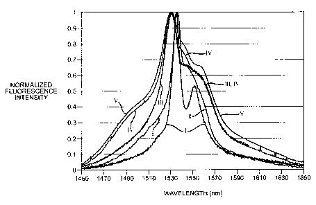
These glasses incorporate a combination of F and Al2O3 to achieve even wider
fluorescence and improved gain flatness. In addition, SPCVD incorporates large
amounts of N into low-loss fiber whose high charge has an impact on rare earth
behavior. The Surface Plasma Chemical Vapor Deposition (SPCVD) produces fiber
preforms with high levels of F, Al2O3, and N. These heavily fluorinated
glasses provide much broader Er3+ emission than Type I or Type II silica for
enhanced multichannel amplifiers. SPCVD successfully fluorinates silica with
losses below 5 dB/km and increased Er3+ emission width.


French Abstract

Les verres de l'invention contiennent une combinaison de F et Al¿2?O¿3? pour obtenir une fluorescence encore plus large et une meilleure planéité du gain. De plus le dépôt par plasma en surface (SPCVD) comprend de grandes quantités de N dans une fibre à faible perte dont la charge élevée a un impact sur le comportement des terres rares. Le dépôt par plasma en surface (SPCVD) produit des préformes de fibres aux niveaux élevés de F, Al¿2?O¿3? et N. Ces verres fortement fluorés produisent une émission Er?3+¿ beaucoup plus large que la silice de type I ou type II pour des amplificateurs multicanaux perfectionnés. Le SPCVD fluore avec succès la silice avec des pertes inférieures à 5 dB/km et une largeur d'émission Er?3+¿ accrue.

Claims

Note: Claims are shown in the official language in which they were submitted.


6
WE CLAIM:
1. A rare earth doped surface plasma chemical vapor deposition fluorine
doped glass comprising:
Component Weight Percent
SiO2 0-95
GeO2 0-95
Al2O3 0-15
Ga2O3 0-15
F 2-10
N 0-10
R2O3 0.01-2.0
with a SiO2+GeO2 range from 80-95 wt.%, an Al2O3+Ga2O3 range from 5-
15 wt.%, and R2O3 is a rare earth oxide, wherein the fluorine doped glass is a
high purity deposited dense glass in which volatile loss of fluorine is
prevented.
2. A glass according to claim 1 wherein F and N range from 2.5 to 5.0
wt.%.
3. A glass according to claim 1 wherein said glass has a 1550 nm loss <
100 dB/km.
4. A glass according to claim 1 containing at least 3 weight percent Al2O3.
5. A glass according to claim 1 wherein R2O3 is a rare earth oxide of Y, La,
Ce, Pr, Nd, Pm, Sm, Eu, Gd, Tb, Dy, Ho, Er, Tm, Yb or Lu.
6. A glass according to claim 1 wherein R is a rare earth oxide of Er, Pr, Eu
or Dy.
7. A glass according to claim 1 wherein R2O3 is Er2O3.

7
8. A glass fiber suitable for use as an optical fiber amplifier comprising the
glass of claim 3.
9. An optical amplifying device comprising the glass fiber of claim 8.
10. An electrical optical device made from the glass of claim 1.
11. A rare earth erbium and fluorine doped surface plasma chemical vapor
deposition glass comprising:
Component Weight Percent
SiO2 0-95
GeO2 0-95
Al2O3 3-15
Ga2O3 0-12
F 2-10
N 0-10
R2O3 0.01-2.0
with a SiO2+GeO2 range from 80-95 wt.%, an Al2O3+Ga2O3 range from 5-
15 wt.%, and R2O3 is Er2O3, wherein the glass is a high purity deposited dense
fluorinated glass formed from an ionizing plasma wherein a loss of volatile
components is prevented.
12. A glass according to claim 1 wherein said glass has a 1550 nm loss <
100 dB/km and an Er3+ emission spectra with a FWHM > 44 nm.
13. A glass according to claim 1 wherein said glass has a 1550 nm loss < 5
dB/km and an Er3+ emission spectra with a FWHM .ltoreq. 50 nm.
14. A glass according to claim 1 wherein said glass has a 1550 nm loss < 5
dB/km and an Er3+ emission spectra with a FWHM .ltoreq. 55 nm.
15. A glass according to claim 1 wherein said glass has a 40 nm Er3+ band
gain ripple less than 20%.

8
16. A glass according to claim 13 wherein said glass has a 40 nm Er3+ band
gain ripple less than 20%.
17. A glass according to claim 1 wherein said glass is simultaneously doped
with F, N and Er with a F- and a N3- substituting for oxygen to form a pseudo-
oxide glass structure.
18. An optical amplifier comprising a glass of claim 16.
19. An optical amplifier comprising a glass of claim 11, said glass having a
1550 nm loss < 5 dB/km, an Er3+ emmission spectra with a FWHM > 44 nm
and a 40 nm Er3+ band gain ripple less than 20%.
20. A method of making a rare earth doped glass that includes providing
rare earth dopant feedstocks and fluorine feedstocks, forming a reaction
plasm, ionizing the feedstocks in the plasma and depositing a dense rare earth
fluorine doped glass wherein the loss of volatile fluorine is prevented.
21. A method of making a rare earth doped optical waveguide amplifier
glass with a broad Er3+ emission spectra FWHM > 44nm and 1550 nm loss <
100 dB/km, that includes providing rare earth dopant feedstocks and fluorine
feedstocks, forming a reaction plasm, ionizing the feedstocks in the plasma
and depositing a dense rare earth fluorine doped glass wherein the loss of
volatile fluorine is prevented.

Description

Note: Descriptions are shown in the official language in which they were submitted.


CA 02367253 2001-09-05
WO 00/55101 PCT/US00/03602
SPCVD SILICATE GLASSES
TECHNICAL FIELD
This invention relates to fluorinated and nitrided silicate glasses made by
Surface Plasma Chemical Vapor Deposition. The new glasses are useful for
gain flattened Er3+ fiber amplifiers. The invention includes making rare earth
doped fluorine containing glasses using plasma chemical vapor deposition.
BACKGROUND ART
Er3+ doped fiber amplifiers have revolutionized optical
telecommunications by providing all-optical high-gain, low-noise amplification
without the need for costly electronic repeaters. However, current amplifiers
are not well suited for multichannel amplification due to the strong
dependence
of their gain as a function of wavelength. The fluorinated aluminosilicate
glasses provide superior gain flatness in the 1530-1560 nm wavelength band
over type I and type I I silica. This enables simultaneous uniform
amplification
of multiple wavelengths for a 4-32x increase in bandwidth in both fiber and
planar devices. This also makes high data rate communication systems
practical and affordable. For example, 16 channels at 10 Gb/s (OC-192
Standard) for 160 Gb/s2 or even 32 channels at 2.4 gb/s (OC-48 Standard) for
76.8 Gb/s total capacity are possible.
Recent developments show that fluorinating Er3+ doped Si02 increases
the fluorescence bandwidth emission at 1550 nm. The art also shows that
AI203 additions increase the fluorescence line width and solubility of Er3+
DISCLOSURE OF INVENTION
Our development incorporates a combination of fluorine, A1203 and/or
Gaz03to achieve even wider Er3+fluorescence and improved gain flatness in
the 1550 nm telecom window. In addition, SPCVD can incorporate large
amounts of F, AI203 and N into low-loss fiber all of which impact rare earth
behavior. The SPCVD produces fiber preforms with high levels of fluorine,
alumina, and nitrogen. These heavily fluorinated glasses provide much

CA 02367253 2001-09-05
WO 00/55101 PCT/US00/03602
2
broader Er3+ emission than Type I or Type II silica for enhanced multichannel
amplifiers. SPCVD successfully fluorinates silica with losses below 5 dB/km
and increased Er3+ emission width.
The rare earth doped glass composition of this invention comprise:
Component Weight Percent
Si02 0-95
Ge02 0-95
AI203 0-15
Ga203 0-15
F 2-10
N 0-10
8203 0.01-2.0
wherein Si02 + Ge02 range from 80-95 wt.%, A1203 + Ga203 range from 5-
wt.%, F range from 2 to 10 wt.% and 8203 is a rare earth oxide. The sums
15 such as Si02 + Ge02 are fully interchangeable. Furthermore, each of Si02
and Ge02 can range from 0-95% as long as the total Si02 + Ge02 is between
80 and 95%.
BRIEF DESCRIPTION OF THE DRAWINGS
Fig. 1 is a graph showing the effect of our invention on Er3+
fluorescence.
Fig. 2 is a graph showing microprobe compositional data of our
fluorinated and nitrated preform.
BEST MODE OF CARRYING OUT INVENTION
Most attempts to fluorine dope alumino silicate soot made by CVD lead
to a stripping of A1203 and Ge02 due to the high vapor pressures of AIF3 and
GeF4. These attempts can not achieve F dopant levels above about 2 wt%F.
However, SPCVD allows for simultaneous co-doping of high levels of fluorine,
up to 5 wt%, and AI203. This achieves an even greater fluorescence line
width and increased rare earth solubility. The SPCVD process deposits dense
glass and not soot. Unlike outside vapor deposition (OVD), this prevents the

CA 02367253 2001-09-05
WO 00/55101 PCT/US00/03602
3
loss of volatile components such as fluorine. The plasma environment creates
a unique chemistry by ionizing the feed stock materials in the plasma. SPCVD
also allows for the incorporation of nitrogen whose effects on Er3+ provides
an
advantage by placing the rare earth in a high field environment.
Wide Er fluorescence emission up to 55 nm FWHM has been achieved
in crucible melted glasses, but crucible melting has not produced fibers with
losses below 100 dB/km. SPCVD makes high fluorine content glasses with
high purity and low loss (<5 dB/km) thereby achieving the width of a crucible
melted glass with the low-loss of CVD glass.
Si02 is the main component of the glass to maintain compatibility with
existing fibers and processing. AI203 additions of greater than 3 wt%
considerably broaden the Er3+ emission, while F additions fill in the 1540 nm
region and further broaden the Er3+ emission envelope.
Preferably, the amount of F plus N ranges from 2.5 to 5.0 wt.%. The
preferred embodiment contemplates only F, only N or the presence of both F
and N.
Doping the glasses with a rare earth metal is desirable for enhancing the
emission and absorption spectra, as discussed above. Therefore, the glasses
of the present invention include an oxide of a rare earth element, such as Y,
La, Ce, Pr, Nd, Pm, Sm, Eu, Gd, Tb, Dy, Ho, Er, Tm, Yb or Lu. Preferably, the
rare earth element is Er, Pr, Eu, or Dy. Even more preferably, the rare earth
element is Er (e.g., Er20g).
The glasses also may contain various other components. For example,
the glasses may further include 0-5 wt.% of other oxides, such as Ta205,
B203, SnO, Zr02, P205, Sb205, As203 or Bi203.
All optical amplifiers, and particularly erbium doped fiber amplifiers have
experienced explosive deployment in fiber optic telecommunication systems
because of the well recognized advantages that these types of devices have
over repeater type amplification schemes. For example, the erbium doped
fiber amplifier (EDFA) conveniently operates in the preferred 1550 nm third
telecommunications spectral window, has high polarization-insensitive gain,
low cross talk between signals at different wavelengths, good saturation
output

CA 02367253 2001-09-05
WO 00/55101 PCT/US00/03602
4
power, and a noise figure close to the fundamental quantum limit. The
excellent noise characteristics potentially allow hundreds of amplifiers to be
incorporated along the length of a fiber telecommunications link which could
then span thousands of kilometers. Optical amplifiers, and particularly EDFAs
in contrast to electronic repeaters, are also transparent to data rate, signal
format and wavelength over a limited range, making them especially useful for
wavelength multiplexed communication systems that simultaneously transmit a
large number of signals using different wavelength bands for each signal.
Example I
Fig. 1 shows the normalized Er3+ emission intensity as a function of
wavelength. The emission spectra of Er3+ in pure Si02 (curve I) is the
narrowest. The additions of fluorine (curve II) and A1203 (curve III)
significantly
broaden the emission from 23 nm to 28 and 44 nm FWHM respectively.
Losses of less than 2 dB/km have been achieved in both systems. By
combining F and AI203, the width is further increased to 50 nm (curve IV). By
adding appropriate glass modifiers such as Ca0 and Ta205 or K20 and
Sb203 emission FWHM in excess of 55 nm can be achieved. Curve V shows
the Er3+fluorescence from a Ca0-Ta205-A1203-Si02glass
Fig. 2 shows that F, N and Er can be simultaneously doped into the
preform. The N3- anion has a high charge that significantly alters the
amplification characteristics. The combination of F and N also are beneficial
since one F- and one N3' can substitute for two 02' to form a pseudo-oxide
structure.
Exam~~le II (Prior Art)
A1203 doping is currently used in Type II EDFA to both increase the
Er3+ solubility and gain flatness over pure Si02. However, these compositions
can only yield a 40 nm band gain ripple of 30% and are prone to
devitrification
at high levels of AI203, greater than a few wt%. The inventive glasses yield a
40 nm band gain ripple of less than 20% and are therefor more desirable for
multichannel EDFA's.

CA 02367253 2001-09-05
WO 00/55101 PCT/LTS00/03602
Fluoride glasses such as ZBLAN (53ZrF4-20BaF2-4LaF3-3AIF3-20NaF
in mole %) are also known for their gain flatness and low phonon energy. They
must be pumped at 1480 nm due to upconversion, and as a result of the 1480
pumping, they have increased noise. They also are extremely difficult to
5 fiberize, are not fusion sliceable, are prone to devitrification and have
poor
durability.
These glasses provide a means for producing low-loss rare earth doped
fiber with improved gain flatness for increased channel capacity. Fiber
produced by this method is fusion spliceable, compatible with existing draw
methods and applicable to both fiber and planar amplifiers.
The invention includes making such rare earth doped surface plasma
chemical vapor deposition fluorine doped glasses by plasma depositing dense
high purity glass wherein loss of volatile glass components is inhibited. A
plasma is created and the plasma environment is utilized to ionize the glass
component feed stock materials which react and form a dense glass deposit
while inhibiting the loss of volatile components, such as fluorine. In
addition to
providing rare earth doped glasses that have beneficial fluorine levels and
fluorine glass compositions since the volatile loss of the volatile fluorine
component is inhibited. The invention also includes incorporating nitrogen
into
such glasses by nitrogen doping using the reactive plasma environment. The
making of such rare earth doped surface plasma chemical vapor deposited
fluorine doped glasses includes the making of optical waveguide amplifier
glass by plasma chemical deposition of rare earth fluorine doped light
amplication glass by inhibiting the volatile loss of volatile glass components
such as fluorine. Such plasma deposition includes providing beneficial high
purity fluorine doped oxide glass chemistry which results in beneficial
optical
amplification properties such as low loss < 100dB/km; <_ 5dB/km in the 1550
nm wavelength region and broad Er3+ emission spectra with FWHMs greater
than 44 nm and 40 nm Er3+ band gain ripple less than 20%.
In addition to these embodiments, persons skilled in the art can see that
numerous modifications and changes may be made to the above invention
without departing from the intended spirit and scope thereof.

Representative Drawing
A single figure which represents the drawing illustrating the invention.
Administrative Status

2024-08-01:As part of the Next Generation Patents (NGP) transition, the Canadian Patents Database (CPD) now contains a more detailed Event History, which replicates the Event Log of our new back-office solution.

Please note that "Inactive:" events refers to events no longer in use in our new back-office solution.

For a clearer understanding of the status of the application/patent presented on this page, the site Disclaimer , as well as the definitions for Patent , Event History , Maintenance Fee  and Payment History  should be consulted.

Event History

Description Date
Inactive: IPC from MCD 2006-03-12
Time Limit for Reversal Expired 2005-02-11
Application Not Reinstated by Deadline 2005-02-11
Deemed Abandoned - Failure to Respond to Maintenance Fee Notice 2004-02-11
Letter Sent 2002-08-23
Inactive: Single transfer 2002-07-02
Inactive: Cover page published 2002-02-22
Inactive: Courtesy letter - Evidence 2002-02-19
Inactive: Notice - National entry - No RFE 2002-02-18
Application Received - PCT 2002-02-07
Application Published (Open to Public Inspection) 2000-09-21

Abandonment History

Abandonment Date Reason Reinstatement Date
2004-02-11

Maintenance Fee

The last payment was received on 2003-01-16

Note : If the full payment has not been received on or before the date indicated, a further fee may be required which may be one of the following

  • the reinstatement fee;
  • the late payment fee; or
  • additional fee to reverse deemed expiry.

Patent fees are adjusted on the 1st of January every year. The amounts above are the current amounts if received by December 31 of the current year.
Please refer to the CIPO Patent Fees web page to see all current fee amounts.

Fee History

Fee Type Anniversary Year Due Date Paid Date
Basic national fee - standard 2001-09-05
Registration of a document 2001-09-05
MF (application, 2nd anniv.) - standard 02 2002-02-11 2002-01-14
MF (application, 3rd anniv.) - standard 03 2003-02-11 2003-01-16
Owners on Record

Note: Records showing the ownership history in alphabetical order.

Current Owners on Record
CORNING INCORPORATED
Past Owners on Record
MATTHEW J. DEJNEKA
ROSTISLAV KHRAPKO
Past Owners that do not appear in the "Owners on Record" listing will appear in other documentation within the application.
Documents

To view selected files, please enter reCAPTCHA code :


To view images, click a link in the Document Description column. To download the documents, select one or more checkboxes in the first column and then click the "Download Selected in PDF format (Zip Archive)" or the "Download Selected as Single PDF" button.

List of published and non-published patent-specific documents on the CPD .

If you have any difficulty accessing content, you can call the Client Service Centre at 1-866-997-1936 or send them an e-mail at CIPO Client Service Centre.


Document
Description 
Date
(yyyy-mm-dd) 
Number of pages   Size of Image (KB) 
Representative drawing 2002-02-20 1 12
Drawings 2001-09-04 2 39
Abstract 2001-09-04 1 56
Description 2001-09-04 5 241
Claims 2001-09-04 3 84
Reminder of maintenance fee due 2002-02-17 1 111
Notice of National Entry 2002-02-17 1 193
Courtesy - Certificate of registration (related document(s)) 2002-08-22 1 112
Courtesy - Abandonment Letter (Maintenance Fee) 2004-04-06 1 175
Reminder - Request for Examination 2004-10-12 1 121
PCT 2001-09-04 5 199
Correspondence 2002-02-17 1 24