Language selection

Search

Patent 2367384 Summary

Third-party information liability

Some of the information on this Web page has been provided by external sources. The Government of Canada is not responsible for the accuracy, reliability or currency of the information supplied by external sources. Users wishing to rely upon this information should consult directly with the source of the information. Content provided by external sources is not subject to official languages, privacy and accessibility requirements.

Claims and Abstract availability

Any discrepancies in the text and image of the Claims and Abstract are due to differing posting times. Text of the Claims and Abstract are posted:

  • At the time the application is open to public inspection;
  • At the time of issue of the patent (grant).
(12) Patent Application: (11) CA 2367384
(54) English Title: AN ARRANGEMENT FOR ENABLING TRIMMING ON A SUBSTRATE AND A METHOD OF PRODUCING A SUBSTRATE THAT ENABLES TRIMMING
(54) French Title: AGENCEMENT PERMETTANT L'AJUSTAGE SUR UN SUBSTRAT ET PROCEDE DE PRODUCTION D'UN SUBSTRAT PERMETTANT L'AJUSTAGE
Status: Deemed Abandoned and Beyond the Period of Reinstatement - Pending Response to Notice of Disregarded Communication
Bibliographic Data
(51) International Patent Classification (IPC):
  • H01C 17/22 (2006.01)
  • H01G 4/224 (2006.01)
  • H05K 1/00 (2006.01)
  • H05K 1/02 (2006.01)
  • H05K 1/11 (2006.01)
  • H05K 1/16 (2006.01)
  • H05K 1/18 (2006.01)
  • H05K 3/02 (2006.01)
(72) Inventors :
  • OLOFSSON, LARS-ANDERS (Sweden)
(73) Owners :
  • TELEFONAKTIEBOLAGET LM ERICSSON
(71) Applicants :
  • TELEFONAKTIEBOLAGET LM ERICSSON (Sweden)
(74) Agent: MARKS & CLERK
(74) Associate agent:
(45) Issued:
(86) PCT Filing Date: 2000-02-18
(87) Open to Public Inspection: 2000-09-21
Examination requested: 2004-12-07
Availability of licence: N/A
Dedicated to the Public: N/A
(25) Language of filing: English

Patent Cooperation Treaty (PCT): Yes
(86) PCT Filing Number: PCT/SE2000/000331
(87) International Publication Number: WO 2000055870
(85) National Entry: 2001-09-10

(30) Application Priority Data:
Application No. Country/Territory Date
9900960-7 (Sweden) 1999-03-17

Abstracts

English Abstract


To enable trimming on a substrate (1) having discrete components (6) that are
surface-mounted on the substrate and/or components (7) that are integrated in
the substrate, a trimmable structure (9) is provided on the surface of the
substrate for each component to be trimmed.


French Abstract

De manière à rendre possible l'ajustage sur un substrat (1) comportant des composants discrets (6) qui sont montés en surface sur ledit substrat et/ou des composants (7) qui sont intégrés audit substrat, la surface dudit substrat comporte une structure (9) susceptible d'être ajustée pour chaque composant à ajuster.

Claims

Note: Claims are shown in the official language in which they were submitted.

6
CLAIMS
1. An arrangement for trimming a discrete capacitor (6) that is surface-
mounted on a
substrate (1), characterized in that it comprises a trimmable capacitor (7)
having a
trimmable first electrode (9) on the surface of the substrate (1), and a
second elec-
trode (8) integrated in the substrate (1), that the first and second
electrodes (9, 8) of
the trimmable capacitor (7) are connected to respective electrodes of the
surface-
mounted discrete capacitor (6) to connect the trimmable capacitor (7) in
parallel
with the surface-mounted discrete capacitor (6).
2. An arrangement for trimming a capacitor that is integrated in a substrate,
charac-
terized in that it comprises a trimmable electrode structure on the surface of
the
substrate, that the trimmable electrode structure is connected to one
electrode of the
capacitor that is integrated in a substrate to form a trimmable capacitor that
is con-
nected in parallel with the capacitor that is integrated in the substrate.
3. An arrangement for trimming an inductor (3) that is surface-mounted on
and/or
integrated in a substrate (1), characterized in that it comprises a trimmable
inductor
structure (4) on the surface of the substrate (1), that the trimmable inductor
structure
(4) is connected in series with the inductor (3) that is surface-mounted on
and/or in-
tegrated in the substrate (1).
4. An arrangement for trimming a resistor (11, 14) that is surface-mounted on
and/or
integrated in a substrate (1), characterized in that it comprises a trimmable
resistor
structure (12, 15) on the surface of the substrate (1), that the trimmable
resistor
structure (12, 15) is series-connected or parallel-connected with the resistor
(11, 14)
that is surface-mounted on andlor integrated in the substrate (1).
5. A method of producing a substrate that enables trimming of a discrete
capacitor
that is surface-mounted on the substrate, characterized by providing a
trimmable

7
capacitor (7) having a trimmable first electrode (9) on the surface of the
substrate
(1), and a second electrode (8) integrated in the substrate (1), and
connecting the
first and second electrodes (9, 8) of the trimmable capacitor (7) to
respective elec-
trodes of the surface-mounted discrete capacitor (6) to connect the trimmable
ca-
pacitor (7) in parallel with the surface-mounted discrete capacitor (6).
6. A method of producing a substrate that enables trimming of a capacitor that
is
integrated in the substrate, characterized by providing a trimmable electrode
structure on the surface of the substrate, and connecting the trimmable
electrode
structure to one electrode of the capacitor that is integrated in a substrate
to form a
trimmable capacitor that is connected in parallel with the capacitor that is
integrated
in the substrate.
7. A method of producing a substrate that enables trimming of an inductor (3)
that is
surface mounted on or integrated in the substrate (1), characterized by
providing a
trimmable inductor structure (4) on the surface of the substrate (1), and
connecting
the trimmable inductor structure (4) in series with the inductor (3) that is
surface-
mounted on and/or integrated in the substrate (1).
8. A method of producing a substrate that enables trimming of a resistor (1 l,
14)
that is surface-mounted on or integrated in the substrate (1), characterized
by pro-
viding a trimmable resistor structure (12, 15) on the surface of the substrate
(1), and
connecting the trimmable resistor structure ( 12, 15) in series or in parallel
with the
resistor (11, 14) that is surface-mounted on and/or integrated in the
substrate (1).

Description

Note: Descriptions are shown in the official language in which they were submitted.


CA 02367384 2001-09-10
WO 00/55870 PCT/SE00/00331
AN ARRANGEMENT FOR ENABLING TRIMMING ON A SUBSTRATE
AND A METHOD OF PRODUCING A SUBSTRATE THAT ENABLES
TRIMMING
TECHNICAL FIELD
The invention relates generally to trimming and more specifically to
functional
trimming and/or component trimming on a substrate having components that are
surface-mounted on the substrate and/or integrated in the substrate.
BACKGROUND OF THE INVENTION
Laser trimming of printed circuit patterns on the surface of a ceramic
substrate is
known per se.
In some applications. there are strict requirements on the physical dimensions
of the
substrate. This has led to a design of so called LTCC substrates (Low
Temperature
Cofired Ceramic substrates) where some components such as resistors, inductors
and capacitors are integrated on different layers of the substrate at the same
time as
there are surface-mounted components mounted on the surface of the substrate.
From JP Patent Abstracts Nos. JP 02052494 A and JP 60194556 A, it is known to
make a hole or a window in multilayer substrates in order to trim a component
mte-
orated on a layer in the substrate. The problem with making a hole or a window
in
the top layer is that too large an area is lost on the top layer where the
surface space
is very restricted.
SUMMARY OF THE INVENTION
The object of the invention is to enable trimming on a multilayer substrate
where
there are very strict requirements on the physical dimensions of the substrate
and es-
pecially the top surface, without having to make holes or windows in the
substrate in
order to free part of the component to be trimmed.

CA 02367384 2001-09-10
WO 00/55870 PCT/SE00/00331
7
This is attained in accordance with the invention in that a trimmable
structure con-
nected to the component to be trimmed, irrespective of whether the component
is
surface-mounted or integrated in the substrate, is provided on the surface of
the sub-
strate for each component to be trimmed.
Both functional trimming and component trimming can be accomplished in this
way.
BRIEF DESCRIPTION OF THE DRAWING
The invention will be described more in detail below with reference to the
appended
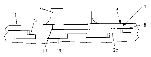
drawing on which Fig.l schematically illustrates a multilayer substrate with a
sur-
face-mounted inductor and a first embodiment of a trimming structure in
accordance
with the invention, Fig. 2 schematically illustrates a multilayer substrate
with a sur-
face-mounted capacitor and a second embodiment of a trimming structure in
accor-
dance with the invention, Fig. 3 schematically illustrates a multilayer
substrate with
a surface-mounted chip resistor and a third embodiment of a trimming structure
in
accordance with the invention, and Fig. 4 schematically illustrates a
multilayer sub-
strate with a surface-mounted discrete component, a resistor integrated in the
sub-
strate, and a fourth embodiment of a trimming structure in accordance with the
in-
vention.
DESCRIPTION OF THE INVENTION
Fig. 1 schematically illustrates a multilayer substrate 1 in which a number of
com-
?5 ponents 2a, 2b, 2c are integrated on different layers.
On the surface of the substrate 1, a discrete component in the form of an
inductor 3
is mounted.

CA 02367384 2001-09-10
WO 00/55870 PCT/SE00/00331
-,
J
In applications where the inductances of the inductors are of so low values
that it is
possible to implement the component as printed conductors in the ceramic
substrate.
most of the conductor pattern is on an inner layer where it does not affect
the sur-
face area of the substrate. To enable trimming of the inductance value, only a
mini-
mal portion of the inductor is located on the surface of the substrate in
accordance
with the invention.
In applications where higher inductance values are required, surface-mounted
in-
ductors have to be used such as the inductor 3 schematically illustrated in
Fig. 1.
In accordance with the invention, the discrete inductor 3 is series-connected
with a
trimmable structure ~ printed on the surface of the substrate 1. In the
embodiment in
Fig. l, the trimmable structure 4 comprises a conductor that is to be laser
trimmed if
necessary.
Since the inductance values of commercially available discrete inductors are
fixed,
the trimmable structure 4 is selected in such a manner that is enables
trimming of
the difference between the commercially available fixed inductance values and
the
area of the trimmable structure on the top layer is designed so it minimizes
the oc-
cupied area.
The trimming structure 4 in Fig. 1 can of course be used to laser trim also
inductors
integrated in the substrate 1.
Thus. e.g. the component 2c in the substrate 1 in Fig. 1 can be an inductor
integrated
on a layer in the substrate 1. To enable trimming of the inductance value of
the in-
ductor 2c by means of the trimming structure 4, the inductors 2c and 4 are
intercon-
nected through a via hole ~ in the top layer of the substrate 1.

CA 02367384 2001-09-10
WO 00/55870 PCT/SE00/00331
Fig. ? illustrates an embodiment of the substrate 1 in Fig. 1 with the
components 2a,
?b and ''c.
In the embodiment in Fig. 2, a discrete capacitor G is surface-mounted on the
surface
of the substrate 1. The capacitor 6 is supposed to be parallel-connected with
a trim-
mable capacitor 7 having one electrode 8 integrated on a layer in the
substrate 1 and
its other electrode in the form of a trimming electrode 9 on the surface of
the sub-
strate 1. The trimming electrode 9 is connected in series with one of the
electrodes
of the surface-mounted discrete capacitor 6.
By means of a trimming structure 9 which is in the form of a conductive area,
it will
be possible to laser trim the capacitances of the capacitors 6 and 7.
The electrode 8 of the capacitor 7, integrated on a layer in the substrate 1,
is con-
nected to the other electrode of the discrete capacitor 6 through a via hole
10 in the
top layer of the substrate 1.
Fia. 3 illustrates another embodiment of the substrate 1 with integrated
components
?a. 2b and ?c.
In the embodiment in Fig. 3, it is supposed that a discrete chip resistor 11
is
mounted on the surface of the substrate 1.
To enable trimming of the discrete resistor 11, a trimmable structure in the
form of a
trimmable resistor 12 is printed on the surface of the substrate 1 and series-
connected with the discrete resistor 11. As indicated in Fig. 3, the trimmable
resistor
1? is connected to other components integrated in the substrate 1 on different
layers.
The trimmable resistor 12 is trimmed by means of conventional laser trimming.
3O

CA 02367384 2001-09-10
WO 00/55870 PCT/SE00/00331
J
Fig. ~. illustrates a further embodiment of the substrate 1 with integrated
components
2a. 2b and 2c.
In the embodiment in Fig. ~l. a discrete component 13 is mounted on the
surface of
the substrate 1. A resistor 14 has been printed on an inner layer of the
substrate 1.
To enable trimming of the resistor 14, a trimmable resistor l~ is printed on
the sur-
face of the substrate 1 and connected in series with the resistor 14 through a
via hole
16 in the top layer of the substrate 1. To trim the resistance value of the
resistor 14,
laser trimming is used to trim the trimmable resistor 15.
It should be obvious from the above, that trimming is easily facilitated using
trim-
mable component structures as described above.

Representative Drawing
A single figure which represents the drawing illustrating the invention.
Administrative Status

2024-08-01:As part of the Next Generation Patents (NGP) transition, the Canadian Patents Database (CPD) now contains a more detailed Event History, which replicates the Event Log of our new back-office solution.

Please note that "Inactive:" events refers to events no longer in use in our new back-office solution.

For a clearer understanding of the status of the application/patent presented on this page, the site Disclaimer , as well as the definitions for Patent , Event History , Maintenance Fee  and Payment History  should be consulted.

Event History

Description Date
Application Not Reinstated by Deadline 2007-02-19
Time Limit for Reversal Expired 2007-02-19
Inactive: IPC from MCD 2006-03-12
Deemed Abandoned - Failure to Respond to Maintenance Fee Notice 2006-02-20
Letter Sent 2005-01-06
Request for Examination Requirements Determined Compliant 2004-12-07
All Requirements for Examination Determined Compliant 2004-12-07
Request for Examination Received 2004-12-07
Inactive: Cover page published 2002-02-25
Inactive: Notice - National entry - No RFE 2002-02-20
Letter Sent 2002-02-20
Application Received - PCT 2002-02-08
Application Published (Open to Public Inspection) 2000-09-21

Abandonment History

Abandonment Date Reason Reinstatement Date
2006-02-20

Maintenance Fee

The last payment was received on 2005-02-09

Note : If the full payment has not been received on or before the date indicated, a further fee may be required which may be one of the following

  • the reinstatement fee;
  • the late payment fee; or
  • additional fee to reverse deemed expiry.

Please refer to the CIPO Patent Fees web page to see all current fee amounts.

Fee History

Fee Type Anniversary Year Due Date Paid Date
MF (application, 2nd anniv.) - standard 02 2002-02-18 2001-09-10
Basic national fee - standard 2001-09-10
Registration of a document 2001-09-10
MF (application, 3rd anniv.) - standard 03 2003-02-18 2003-02-04
MF (application, 4th anniv.) - standard 04 2004-02-18 2004-02-04
Request for examination - standard 2004-12-07
MF (application, 5th anniv.) - standard 05 2005-02-18 2005-02-09
Owners on Record

Note: Records showing the ownership history in alphabetical order.

Current Owners on Record
TELEFONAKTIEBOLAGET LM ERICSSON
Past Owners on Record
LARS-ANDERS OLOFSSON
Past Owners that do not appear in the "Owners on Record" listing will appear in other documentation within the application.
Documents

To view selected files, please enter reCAPTCHA code :


To view images, click a link in the Document Description column. To download the documents, select one or more checkboxes in the first column and then click the "Download Selected in PDF format (Zip Archive)" or the "Download Selected as Single PDF" button.

List of published and non-published patent-specific documents on the CPD .

If you have any difficulty accessing content, you can call the Client Service Centre at 1-866-997-1936 or send them an e-mail at CIPO Client Service Centre.


Document
Description 
Date
(yyyy-mm-dd) 
Number of pages   Size of Image (KB) 
Representative drawing 2002-02-22 1 4
Cover Page 2002-02-25 1 32
Claims 2001-09-10 2 95
Abstract 2001-09-10 1 45
Drawings 2001-09-10 2 16
Description 2001-09-10 5 167
Notice of National Entry 2002-02-20 1 193
Courtesy - Certificate of registration (related document(s)) 2002-02-20 1 113
Reminder - Request for Examination 2004-10-19 1 121
Acknowledgement of Request for Examination 2005-01-06 1 176
Courtesy - Abandonment Letter (Maintenance Fee) 2006-04-18 1 177
PCT 2001-09-10 9 371