Note: Descriptions are shown in the official language in which they were submitted.
CA 02367407 2001-09-07
1
WO 00/69096 PCT/US00/08113
SYSTEM AND METHOD FOR ESTIMATING POWER
BACKGROUND OF THE INVENTION
I. Field of the Invention
The present invention relates generally to mobile communication
systems. More particularly, the present invention relates to a system and
method for estimating the power of a communication signal or set of signals
forming a subbeam. The present invention is most applicable in a mobile
communications system using satellites where keeping track of satellite
power is critical.
II. Related Art
A satellite-based communications system is a means by which
information is sent over a substantial distance. Typical satellite-based
communications systems use base stations referred to as gateways, and one
or more satellites to relay communications signals between the gateways and
one or more user terminals. Gateways provide communication links from
each user terminal to other user terminals or users of other connected
communications systems, such as a public telephone switching network.
The user terminals can be fixed or mobile, such as a mobile telephone, and
are located anywhere they can communicate with a satellite.
A satellite transponder is the component in a satellite that receives
and transmits signals from and to gateways and user terminals. A satellite
transponder must be able to carry a large number of subscribers
simultaneously in order to be cost effective. Various satellite access schemes
such as time division multiplex access (TDMA) and code division multiplex
access (CDMA) spread spectrum allow access to transponders by a large
number of subscribers. Digital CDMA is preferable to other satellite access
schemes as more communication signals can be carried at a lower cost and
higher quality. This is due in part because CDMA systems enable use of low
powered signals which minimize cross channel interference and conserve
satellite power.
CA 02367407 2001-09-07
WO 00/69096 PCT/US00/08113
In a typical spread-spectrum communication system, preselected
pseudorandom noise (PN) code sequences are used to modulate or 'spread'
user information signals over a predetermined spectral band prior to
modulation onto a carrier for transmission as communication signals. PN
spreading is a method of spread-spectrum transmission that is well known
in the art.
In a typical CDMA spread-spectrum communication system,
channelizing codes are used to discriminate between signals for different
users within a cell or between user signals transmitted within a satellite
beam, or sub-beam, on a forward link (i.e., the signal path from the base
station or gateway to the user transceiver). That is, each user transceiver
In a CDMA system each customer, subscriber, or user terminal is
assigned an individual, orthogonal, communications channel by using
'covering' or 'channelizing' orthogonal codes. Walsh functions are
generally used to implement the channelizing codes, with a typical length
being on the order of 64 code chips for terrestrial systems and 128 code chips
for satellite systems. CDMA systems combine individual code channels into
a single narrowband channel so that a large number of channels are spread
throughout the same waveform. As a result, multiple customers or users
simultaneously share the same "narrowband channel," ~n~hich is referred to
interchangeably herein as a "CDMA channel" "subbeam" or a "carrier".
Because multiple customers or users share the use of the same subbeam, if
one or more customer or user signals are transmitted at a higher power than
signals intended for other customers or users on the channel, interference
may occur which may result in unacceptable performance unless the
number of users on the subbeam is reduced. More importantly, such extra
power reduces the power available for other user signals and, thus, overall
capacity.
In a typical CDMA system, a gateway and a satellite communicate via
links which are spatially divided into a number of beams, for example 16, in
both a forward and a return direction, referred to as links. On the forward
link, information is transmitted by a gateway generally utilizing frequency
division and polarization multiplexir~;. In an exemplary system design, the
CA 02367407 2001-09-07
WO 00/69096 PCT/US00/08113
3
forward link uses a C-band frequency band that is divided into 8 individual
16.5 MHz "channels" or "beams" employing right hand circular polarization
(RHCP) and 8 individual 16.5 MHz "channels" or "beams" employing left
hand circular polarization (LHCP). These individual 16.5 MHz channels are
in turn made up of 13 "subchannels" or "subbeams," each of 1.23 MHz
bandwidth, that are frequency division multiplexed (FDM) together to form
a beam. These FDM subbeams are the narrowband channels discussed
above, formed by combining a number of code channels.
For transmission to a satellite, individual FDM subbeams are
frequency multiplexed together to create one wideband channel. A
wideband channel has a pre-selected bandwidth designed for the specific
satellite system. In the present example, a bandwidth of 160 MHz is used
which comprises 104 subbeams, 13 subbeams times 8 beams. The ability of a
wideband channel to carry 104 subbeams is dependent on limiting the power
of each subbeam to the minimum power necessary for high quality
transmission. Thus, control of the power of the subbeams is needed for high
quality transmission and to ensure efficient use of power which allows the
maximum number of subbeams to be carried on a wideband channel.
A system and method for controlling the gain of individual
narrowband channels (subbeams) using a wideband power measurement
has been developed. That system and method uses a transmit power
tracking loop (TPTL) to control the power of individual narrowband
channels (subbeams) by adjusting the gain applied to a transmitted signal.
This system and method is disclosed in U.S. Patent Application Serial No.
09/150,545, entitled S~steni and Method for Gain Control Of Individual
Narrowbc~nd Channels Using A Wideba~zd Power Measurement, which is
assigned to the assignee of the present invention, and incorporated, in its
entirety, herein by reference. Both open loop and closed loop power control
are used in the TPTL. The closed loop control requires the control of the
power of each individual subbeam. To control the power of each subbeam it
is necessary to determine the power of each subbeam. However, difficulties
arise in measuring individual subbeam po~~er in the time frames needed to
effectively control gain. In addition, performing such po~n~er estimation can
CA 02367407 2001-09-07
WO 00/69096 PCT/US00/08113
4
be very computationally intensive, especially for control software
implementations. As a result, there is a need for an alternative system and
method for determining or estimating the power of individual subbeams.
Determinations of the power of individual subbeams can also be used
to monitor the power consumption of a satellite receiving the subbeams.
The satellite requires power to receive and relay the subbeams. The satellite
is powered by batteries which store solar energy collected by the solar
panels.
Because the satellite only charges while exposed to the sun, the power of the
satellite is limited by the exposure of the satellite to the sun.
Because of the limited energy in a satellite, it is possible that the
satellite can run out of energy. Thus, in order to properly operate the
satellite, it is necessary to know how much energy is being used by each
transmitted subbeam. For example, in order to divide up capacity among
service providers, it is necessary to know the amount of power used in
transmitting on an individual subbeam basis. Also, to protect the satellite
from damage by overdriving the satellite, it is necessary to know how much
power is being transmitted on each subbeam.
Proper management of the satellite battery is vital to the longevity of
the satellite constellation. The energy removed from the battery in order to
process traffic must be replenished during the charging time when the
satellite is in the sun. If too much energy is removed to process the traffic,
the satellite must stay in the sun longer or must tap the batteries' reserve
power. The operating life of the batter~~ is degraded when the battery reserve
power is accessed. The quality of satellite energy estimation is in part a
function of the estimation of the power of each subbeam. More specifically,
power usage of a satellite can be measured by measuring the power of signals
sent to the satellite. This is because a satellite transponder transmits
signals
at a power that is proportional to the power of the signals received by the
transponder.
Thus, there is a need to estimate the power of each subbeam that is
transmitted from a gate~~ay to a satellite. These power estimates can be used
to determine power consumption and can be used in control systems that
adjust the po~n~er of each subbeam. More specifically there is a need to
CA 02367407 2001-09-07
WO 00/69096 PCT/US00/08113
estimate the power of subbeams in order to keep track of the power
consumption of and availability i n-a satellite. Additionally, there is a need
to estimate the power of each subbeam in order to limit the power of each
subbeam. Also, there is a need to estimate the power of subbeams in order to
5 allocate capacity among service providers and to provide billing
information. Furthermore, there is a need to estimate the power of
subbeams in order to avoid overdriving satellites and to avoid violating flux
density limits.
The system for estimating power should consume a minimal amount
of power and have a low degree of complexity so that it occupies a minimal
amount of space. This is because the size of integrated circuits or chips used
to implement the power estimation system and the amount of power that a
chip can handle may be limited. In addition, the larger a chip, i.e, the more
logic gates on the chip, the more expensive the chip is to produce. Also, the
more logic gates on a chip, the more power is required to drive the gates.
Because a chip can only dissipate so much power, a chip with too many logic
gates may also produce too much thermal energy, causing the chip to fail.
Additionally, the more power required to drive a chip, the more expensive it
is to drive the chip. Therefore, reducing the number of logic gates on a chip
may reduce the cost of producing and powering the chip and increase the
reliability of the chip.
SUMMARY OF THE INVENTION
The invention concerns a system and method for estimating the
power of a signal in a satellite communications system. The signal is
compared to and separated into a plurality of ranges by a separating means.
Each range is assigned a particular output value. The output values
approximate the square of the input signal based on knov~~n characteristics of
the input signal. A low pass filter is used to average a plurality of the
output
values. In one embodiment, the low pass filter comprises an infinite
impulse response filter.
CA 02367407 2001-09-07
WO 00/69096 PCT/US00/08113
6
A feature of the present invention is that when the input signal is
represented by a predetermined number of bits, the assigned output values
are represented by a number of bits which is less than twice the
predetermined number of bits.
Another feature of the present invention is that when the input
signal is represented by a predetermined number of bits, the assigned output
values are represented by a number of bits which is less than the
predetermined number of bits.
Another feature of the present invention is that when the input
signal is produced by an I channel or a Q channel of a Quadriphase Phase
Shift Key (QPSK) modulator, the total power of a signal created by the
modulator can be determined based on a ratio of the I channel power to the
Q channel power.
An additional feature of the present invention is that the output of
the separating means represents an instantaneous power of the input signal
and an output of the filter represents an average power of the input signal.
Still another feature of the present invention is that the output of the
separating means is proportional to an instantaneous power of the input
signal and an output of the filter is proportional to an average power of the
input signal.
BRIEF DESCRIPTION OF THE DRAWINGS
FIG.1 illustrates an exemplary implementation of communication
links used between a gateway and a user terminal in a mobile
communications system.
FIG. 2A is a high level block diagram of a system for measuring the
power of a signal according to the present invention.
FIG. 2B is a high level block diagram of a system that estimates the
power of a signal using 12 bit samples of the signal according to the present
invention.
FIG. 3 is a high level block diagram illustrating a system for estimating
the power of a signal according to an embodiment of the present invention.
CA 02367407 2001-09-07
WO 00/69096 PCT/US00/08113
7
FIG. 4 is a high level block diagram illustrating a system for estimating
the power of a signal according to an embodiment of the present invention.
DETAILED DESCRIPTION OF THE PREFERRED
EMBODIMENTS
The present invention is a system and method for estimating the
power of a signal, such as one represented by either time varying voltage or
current values. An instantaneous power of the signal can be determined by
squaring a quantized representation of the signal. This is because power is
proportional to the square of the voltage. The average power over time can
then be determined based on these instantaneous power determinations. A
digital squaring circuit can be used to square the signal. A low pass filter
can
be used to average the output of the squaring circuit.
In digital implementations, a squaring circuit output requires twice as
many bits as the input if precision is not to be lost. This output,
representing
instantaneous power, is input into a low pass filter to average the power
over time. Depending on the number of bits used to represent the input
signal, the squaring circuit can be prohibitively large in terms of logic
gates
and can consume too much power. Furthermore, with many bits
representing the squared output, a low pass filter following the squaring
circuit may require a large number of bits internal to the filter to keep
quantization noise from dominating the filter's output for all possible
inputs. Also, a long filter time constant, relative to the reciprocal of the
sample rate, can result in instability if too few bits are used to represent
the
feedback branches.
The present invention utilizes a sparse lookup table (LUT) to replace
the squaring circuit discussed above. More specifically, the sparse lookup
table is used to separate an input signal into a plurality of ranges, wherein
each range is assigned a particular output value. These output values
approximate the square of the input signal based on known characteristics of
the input signal. The number of bits required to represent these output
values can be greatly reduced by using the known characteristics of the input
CA 02367407 2001-09-07
WO 00/69096 PCT/US00/08113
8
signal when selecting the plurality of ranges in the sparse LUT and knowing
the required accuracy of the estimation.
By reducing the number of bits that represent the output, a low pass
filter used to average the instantaneous power estimates can be more easily
built on an integrated circuit chip with a reasonable number of bits internal
to the filter. Additionally, the sparse LUT can be digitally implemented
using less logic gates than a squaring circuit, which results in less power
consumption and a smaller overall digital circuit size. By reducing the
number of logic gates on a chip, the cost of producing and powering the chip
may be reduced and the reliability of the circuit or chip may be increased.
Among other uses, the present invention could find use in a variety
of wireless communication systems including satellite based telephone
systems. In the preferred embodiment, the present invention is directed to
estimating the power of a subbeam transmitted from a gateway to a satellite.
More specifically, a preferred application is in Code Division Multiple Access
(CDMA) wireless spread spectrum satellite communications systems. Below
is an overview of a system in which the present invention may be used.
I. System Overview
FIG. 1 illustrates an example implementation of communication links
used between gateway 102 and user terminal 104 of communications system
100. It is contemplated that communications system 100 uses CDMA type
communication signals, but this is not required by the present invention. In
the portion of communication system 100 illustrated in FIG. 1, satellite 106
and associated gateway 102 are shown for effecting communications with
remote user terminal 104. The total number of gateways and satellites in
such a system depends on the desired system capacity and other factors well
understood in the art.
Communications links between user terminal 104 and satellite 106 are
termed user links and the links between the gate~~ay 102 and the satellite 106
are termed feeder links. Communication proceeds in a "forward" direction
from gateway 102 on forward feeder link 110 and then down from satellite
106 to user terminal 104 on forward user link 112. In a "return" or "reverse"
CA 02367407 2001-09-07
WO 00/69096 PCT/US00/08113
9
direction, communication proceeds up from user terminal 104 to satellite
106 on return user link 114 and then down from satellite 106 to gate~~ay 102
on return feeder link 116.
On forward link 110 information is transmitted by gateway 102
utilizing frequency division and, where used, polarization multiplexing. As
discussed above, in an example embodiment, the frequency band used is
divided into 8 individual 16.5 MHz "channels" or "beams" using right hand
circular polarization (RHCP) and 8 individual 16.5 MHz "channels" or
"beams" using left hand circular polarization (LHCP). These individual 16.5
MHz channels are in turn made up of a set of frequency division
multiplexed (FDM) "subchannels" or "subbeams", each of 1.23 MHz
bandwidth. In the present example, there are up to 13 such subchannels,
however more or fewer could be used, as is well known. Each FDM
subbeam is created by a separate modulator circuit, and has an associated
channel or beam power. Each FDM subbeam is divided into user channels
using orthogonal codes in CDMA type spread spectrum systems, or time
slots using TDMA type systems. The present invention is not limited by the
specific type of channel modulation. In a CDMA communication system,
each of the code channels, for example one of 128 Walsh covered channels,
represents power consumed to service a user on the forward link. Some of
the orthogonal code channels may also be used by pilot signals, which
provide phase reference and timing references, and other overhead signals.
In the reverse direction, user terminal 104 transmits according to a
spatially divided beam pattern. Satellite 106 receives these signals and
frequency division multiplexes them for the satellite-to-gateway feeder link
106.
II. Gateway
Gateway 102 provides a communication link using satellite 106
between user terminals 104 and a local mobile telephone switching office
(MTSO) (not shown), a public switched telephone network (PSTN) (not
shown), or other connected communication system, as desired, as is well
known. Gateway 102 receives telephone calls, data and/or fax data, or other
CA 02367407 2001-09-07
WO 00/69096 PCT/US00/08113
information intended for a system user from the local MTSO or the PSTN
and generates the code channels, subbeams, and beams discussed above to
transmit to satellite 106. Satellite 106 then re-transmits these signals to
one
or more user terminals 104. In the return or reverse link direction, gateway
5 102 receives voice, data, fax data, or other information transmitted from
user
terminal 104, using satellite 106, and connects the user communication link
or call to a MTSO or PSTN, which can then connect user terminal 104 to a
standard telephone system, another mobile telephone system, or other
known types of connected communication systems.
10 Gateway 102 modulates and transmits signals intended for user
terminals, that arrive for example from a PSTN or the MTSO, to user
terminal 104 via satellite 106. Gateway 102 also receives and demodulates
signals from satellite 106. Transmission circuitry or equipment in gateway
102 includes modulators which generate subbeams. These modulators
receive channel data and spread spectrum modulate the channel data. The
modulated signal is then sent to an upconverter. Each modulator in
gateway 102 is connected to a corresponding upconverter for upconverting
the modulated signal from intermediate band frequency (IF) to a desired
radio band frequency (RF). The upconverters are connected to an input of a
summer which sums the individual subbeam signals into a widebeam
signal. For additional details of a modulator see U.S. Patent No. 5,103,459,
entitled "System and Method for Generating Signal Waveforms in a CDMA
cellular Telephone System," which is incorporated by reference herein.
Although not limited to this use, the present invention may be used to
estimate the power of these subbeams.
III. Satellite
Satellite 106 is one of a number of satellites that comprise a low earth
orbiting (LEO) satellite system. An exemplary LEO satellite system is
planned to include 48 or more satellites traveling in low earth orbits
approximately 763 miles form the earth's surface and inclined 50 degrees
from the equator. In addition to LEO satellites, any communications device
that receives and transmits information from and to an antenna, including
CA 02367407 2001-09-07
WO 00/69096 PCT/US00/08113
11
satellite systems located at other distances and orbits, may be used with the
present invention.
Satellite 106 receives and demultiplexes the signals, which may be
transferred using two orthogonal polarizations, to obtain M individual
signals each of a preselected bandwidth which corresponds to a desired
spatially separated beam pattern. Typically, there are 16 signals or beams
(M=16) for a satellite footprint each having a 16.5 MHz bandwidth,. As
mentioned above, each "beam" contains or is further divided into 13
"subbeams" operating on separate frequencies. Thus, satellite 106 handles
approximately 208 (16 x 13) subbeams. However, those skilled in the art will
readily understand that fewer or more beams and sub-beams can be
employed according to each communication system and satellite
constellation design.
Satellite 106 requires power to receive and relay the subbeams.
Satellite 106 is powered by batteries which store solar energy collected by
solar panels 120. Satellite 106 only charges while exposed to the sun. Thus,
the power of satellite 106 is limited by its exposure to the sun. ~ Because
satellite 106 has limited energy, it is possible that satellite 106 can run
out of
energy. Thus, in order to properly operate satellite 106 it is necessary to
know how much energy is being used by satellite 106 over any given time
period. Power usage of satellite 106 can be measured by measuring the
power of signals sent to satellite 106. This is because each satellite
transponder transmits a signal having a power which is proportional to the
power of the signal that was received by the satellite or transponder.
As stated above, satellite 106 has a transponder that transmits
subbeams down to user terminals and gateways. The power used by the
satellite transponder can be determined if the power of subbeams sent to
satellite 106 is known. Because a transponder generally responds predictably
to the amount of power in the signal it receives, controlling the power levels
of signals sent from gateway 102 controls how much power satellite 106 uses.
The distance between gateway 102 and satellite 106 can be determined from
location identifying information sent to gateway 102 by satellite 106. By
kno~~ing that distance, the gain of a satellite transponder, and antenna gain,
CA 02367407 2001-09-07
WO 00/69096 PCT/US00/08113
12
a desired or optimal amount of power for a signal sent from gateway 102 to
satellite 106 can be determined. The estimated power of a subbeam
determined using the present invention can be used to optimally adjust the
power of the subbeam. It is noted that the specific method of optimizing or
determining optimal power of a subbeam is beyond the scope of this
invention. Additionally, the specific method the determining the power
usage of the satellite based on the power of subbeams sent to the satellite is
beyond this scope of this invention, and relates to techniques know to those
skilled in the art of satellite design and operation.
It is also necessary to know the amount of power used in transmitting
on an individual subbeam basis in order to divide up capacity among service
providers. Since satellite power is the scarce resource in a satellite
communications system, power consumption can be the basis for billing
service providers for their use of satellite 106 (for example, service
providers
can pay more for more power). More specifically, if service providers are
allocated capacity on a subbeam basis, measuring the power of each subbeam
can provide useful billing information.
Also, to protect the satellite from damage due to over driving of the
satellite, it is necessary to know how much power is being transmitted on
each channel. Power must also be measured and controlled to avoid
violating flux density limits.
IV. Power Estimator
One method for estimating the power of a voltage waveform includes
sampling the waveform, inputting the samples into a squaring circuit, and
then filtering the output of the squaring circuit. FIG. 2A is high level block
diagram of a system that uses such a method. As shown, sampled waveform
202 is input into squaring circuit 204. Squaring circuit output 206 of
squaring
circuit 204 is input into filter 208. Filter output 210 of filter 208
represents the
averaged power of sampled waveform 202.
It is necessary that the samples of a waveform have enough
resolution to meet the desired accuracy requirements for the estimation. For
the purpose of example, «~e shall assume that a 12 bit sample of the
CA 02367407 2001-09-07
WO 00/69096 PCT/US00/08113
13
waveform provides sufficient resolution. The 12 bits represent the voltage
(amplitude) of the waveform when the waveform is sampled. Because the
samples are 12 bits in length, there are 21' (4096) different levels which can
be
represented. These different levels are scaled to a maximum voltage level.
For example, if the maximum voltage is 2 Volts and the minimum voltage
is -2 Volts, then a range of 4 Volts exists. Considering 4 = 4096 = 9.8*10~
then
the accuracy of the sample is ~ 4.9*10-~ Volts. This well known process of
separating the amplitude of the waveform into a prescribed number of
discrete amplitude levels is called quantization. The resultant waveform is
said to be quantized.
FIG. 2B is a high level block diagram of a system that estimates the
power of a voltage waveform using 12 bit samples of the waveform. As
shown, sample waveform 212 input into squaring circuit 214 is 12 bits in
length. To represent the square of 12 bits, up to 24 bits may be required.
That
is, in digital implementations, a squaring circuit output requires twice as
many bits as the input if precision is not to be lost. Thus, output 316 of
squaring circuit 214 is shown to be 24 bits. This output represents the
instantaneous power. As a result of requiring 24 bits, the squaring circuit
can
be prohibitively large in terms of logic gates and can consume too much
power. Furthermore, with many bits representing the squared output, a low
pass filter 218 following squaring circuit 214 requires a large number of bits
internal to filter 218 to keep quantization noise from dominating filter
output 220 for all possible inputs. As stated earlier, a long filter time
constant, relative to the reciprocal of the sample rate, can result in
instability
if too few bits are used to represent the feedback branches.
Filter 218, generally a low pass infinite impulse response (IIR) filter, is
used to average output 216 of squaring circuit 214. More specifically, filter
218 limits the bandwidth of the instantaneous power waveform produced by
squaring circuit 214. To illustrate the large number of bits used to represent
feedback branches within filter 218, the number of bits is shown above each
branch. As can be seen, with 24 bits representing squared output 216, low
pass IIR filter 218 following squaring circuit 214 requires a large number of
bits internal to the filter to keep quantization noise from dominating filter
CA 02367407 2001-09-07
WO 00/69096 PCT/US00/08113
14
output 220 for all possible inputs. Also, because filter 218 may have a long
time constant, relative to the reciprocal of the sample rate, use of less bits
to
represent the feedback branches can result in instability.
Other types of low pass filters can be used besides an IIR type filter to
implement filter 218 as would be understood by those skilled in the art.
However, in a preferred embodiment filter 218 is an IIR filter comprising
multiples of two branch weights. By using only multiples of two branch
weights, all gain stages internal to IIR filter 218 can be implemented as
shift
registers. Additionally, because an IIR filter uses feedback, fewer logic
gates
are required to build the filter, for example when implemented on an
integrated circuit chip. However, a disadvantage of using feedback is the
introduction of the possibility of instability. This is because the use of
feedback subjects the filter to oscillations and limit cycles, as is known. To
prevent instability, enough bits must be maintained internal to the filter so
that when there are oscillations they are small in magnitude.
Another type of filter which may be used is a finite impulse response
(FIR) filter, which does not use feedback. One advantage of an FIR filter is
that it is more stable than a IIR filter. However, the use of a FIR filter may
be
impractical, or at least less than optimal. Because a FIR filter does not use
feedback, to have the capability of averaging many samples (e.g., thousands)
the FIR filter would need to be extremely large in terms of the number logic
gates required, again increasing size, cost, and complexity.
FIG. 3 is a high level block diagram illustrating an embodiment of the
present invention. A significant difference between FIG. 2B and FIG. 3 is
that squaring circuit 214 of FIG. 2B is replaced with a circuit functioning as
a
sparse, or coarse, look-up table (LUT) 304. An example of a transfer function
for LUT 304 is shown in Table 1 below.
CA 02367407 2001-09-07
WO 00/69096 PCT/US00/08113
TABLE 1
Input Range, LUT Output, f(X)
X
~X~ - 0 0
0< ~X~ <14 1/1024
14<_~X~ <20 2/1024
20<_~X~ <62 4/1024
62<_~X~ <75 6/1024
75 <_ ~ < 120 46/1024
X ~
120 <_ ~ < 165 110/1024
X ~
165_<~X~ <320 114/1024
320 <_ ~ 900/1024
X ~
The transfer function can be established through experimentation and
5 thorough knowledge of input waveform 302 statistics. For the present
example, the use of 10 bits to represent squared output 306 is based o n
shortcuts which can be taken and knowledge of the system. For example, if
input waveform 302 is a CDMA waveform, and it is known that a CDMA
waveform has a Gaussian distribution, a transfer function can be created
10 having the desired accuracy. More specifically, by knowing that a
distribution is Gaussian, a transfer function can be created where more
accuracy is dedicated to values near a mean and less accuracy is dedicated to
values far from the mean. Additionally, the transfer function can take into
account that waveforms with small variances consume small amounts of
15 satellite power, and, thus, the allowable error for these small waveforms
is
greater than for higher power waveforms.
The transfer function of Table 1 is for an input signal X having a
mean of 0. As can be seen from Table 1, six different outputs exist for input
signals having an absolute value range between 0 and 120, only two outputs
exist for signal inputs having an absolute value range between 120 and 320,
and only one output exists for input signals having an absolute value greater
than or equal to 320. Thus, we can tell from Table 1 that it is most probable
CA 02367407 2001-09-07
WO 00/69096 PCT/US00/08113
16
that the absolute value of input signal X is bet~~een 0 and 120 and it is
least
probable that signal X is above 320.
Each range in Table 1 may be referred to as a "bin". That is
"14 _< ~ X ~ < 20" is one bin, and "62 <_ ~ X ~ < 75" is another bin. Table 1
consists
of only nine bins. When averaging the estimated power of a large number
of samples, the accuracy of the power estimate of each sample need not be
great so long as the integrated sum of the estimates provides the required
accuracy. This allows use of a small number of bins or ranges (e.g., nine bins
in the above example). The less bins there are, the less logic gates are
required to implement a function.
As discussed above, Table 1 is generally optimized for Gaussian
distributed input waveforms. So long as the input waveforms represent a
large number of users, (a condition which results in significant power
consumption) the assumption of a Gaussian waveform is justified.
However, the present invention is not limited to signals having a Gaussian
distribution. The present invention can be used for any signal having a
distribution which is predictable. Examples of other distributions include
sinusoidal distribution and uniform distribution. Using any of these
distributions, a LUT similar to Table 1 can be optimized to produce a desired
accuracy using a relatively small number of logic gates.
A circuit implementing Table 1, i.e., LUT 304, can be built in the form
of a single integrated circuit or "chip" using comparators and/or other
known logic gates, referred to as built "on-chip." In one embodiment, the
circuit can be designed and built using Very High Speed Integrated Circuit
(VHSIC) Hardware Description Language. VHSIC is a known large high-
level VLSI design language used for determining a theoretically optimal gate
arrangement for building a circuit on-chip.
Reducing output 306 to only 10 bits, as compared to 24 bits, allows low
pass filter 308 to be built on-chip with a reasonable number of bits internal
to
filter 308. To illustrate the reduction in the number of bits used to
represent
feedback branches within filter 308, as compared to filter 208 above, for each
branch within filter 308 the number of bits is shown. Bv reducing the
CA 02367407 2001-09-07
WO 00/69096 PCT/US00/08113
17
number of logic gates on-chip, the cost of producing and powering the chip
may be reduced and the reliability of the chip may be increased.
The present invention is not limited by the number of bits which
represent inputs and outputs. Rather the present invention is only limited
by the required or desired accuracy of the power estimation and the required
number of bits to maintain stability within the particular filter being used.
The present invention can be used to estimate the power of any
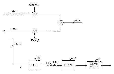
signal. However, in the preferred embodiment, the present invention is
used to estimate the power of a subbeam, or CDMA channel in a
communication system, such as one using satellites. FIG.4 is a block
diagram of the preferred embodiment of the present invention. FIG.4 is
similar to FIG. 3 in that LUT 404 is essentially the same as LUT 304, and
filter
408 is essentially the same as filter 308. Prior to describing FIG. 4, a brief
summary of a CDMA system is provided.
CDMA spread spectrum systems are well known in the art. By using
PN code spreading, a method of spread-spectrum transmission that is well
known in the art, a CDMA system produces a signal for transmission that
has a bandwidth much greater than that of the data signal. More specifically,
to create a subbeam, one or more preselected pseudo-noise (PN) code
sequences are used to modulate or "spread" user information signals over a
predetermined spectral band prior to modulation onto a carrier for
transmission as communications signals. Details of creating a subbeam are
described in the previously mentioned '459 patent. However, for the
purpose of completeness, an example of a CDMA spread spectrum system is
described below.
In a typical CDMA spread spectrum system, orthogonal channelizing
codes are used to discriminate between different user signals transmitted
within a subbeam on the forward link (i.e., the signal path from the gateway
to a user terminal's transceiver). Walsh functions are generally used to
implement the channelizing codes. Each orthogonally, Walsh, coded user
signal is then put through a gain control element. Following the gain
control element all of these signals are then summed together to form one
composite data stream. This composite data stream is then split into two
CA 02367407 2001-09-07
WO 00/69096 PCT/US00/08113
18
data streams, one for an in-phase channel (I channel) and one for a
quadrature phase channel (Q channel) of a Quadrature Phase Shift Key
(QPSK) modulator. QPSK modulators are well known in the art. However,
for completeness, QPSK modulation is briefly described. Each data stream
(one on the I channel, one on the Q channel) is multiplied by separate PN
sequences. Following the multiplication by the PN sequences the I channel
data and the Q channel data are each upconverted 90 degrees out of phase
from one another, by cosine and sine signals respectively, and then added
together to produce one composite waveform. This composite waveform is
a subbeam.
As shown in FIG.4, and as described above, in-phase channel (I
channel) 414 and quadrature phase (Q channel) 412 are produced within the
modulator. The resulting signals are summed to form a subbeam. In QPSK
waveforms, if the ratio of power between the I and Q channel is known,
measuring the power of the I channel (or the Q channel) is enough to
estimate the total signal power. In a preferred embodiment, the power of a
subbeam is determined by estimating the power of only I channel 414 or Q
channel 412. Then, using a known or measured ratio between the power of I
channel 414 and Q channel 412, the total power of the combined signal 416
(that is, the subbeam) can be determined. In a preferred embodiment, the
ratio of I channel 414 to Q channel 412 is 1:1. Thus, in the preferred
embodiment the total power would be twice the estimated power of either I
channel 414 or Q channel 412. Of course the ratio need not be 1:1, as would
be readily understood by those skilled in the art, and depends on each
desired communication system design.
More specifically, as shown in FIG. 4, the 12 bit samples representing
voltage of Q channel 412 signal are input into sparse LUT 404. Output 406 of
LUT 404, represented by 10 bits, is input into low pass filter 408. In the
preferred embodiment, filter 408 is a IIR filter equivalent to filter 308
discussed above. The output of filter 408 represents the average power of Q
channel 412. The power of summed sib al 416 of both I channel 414 and Q
channel 412 can then be determined based on the ratio between the two
channels 414, 412. This summed signal 416 is a subbeam.
CA 02367407 2001-09-07
WO 00/69096 PCT/US00/08113
19
While various embodiments of the present invention have been
described above, it should be understood that they have been presented by
way of example only, not limitation. Thus, the breadth and scope of the
present invention should not be limited by any of the above-described
exemplary embodiments, but should be defined only in accordance with the
following claims and their equivalents.
What I claim as my invention is: