Note: Descriptions are shown in the official language in which they were submitted.
01-09-12 16:17 TO-SMART FROM-IKEUCHI.SATO & PARTNER PATENT ATTORNEYS T-456
P.05 F-935
CA 02368171 2001-09-14
DESCRIPTION
INFORMATION RECORDING MEDIUM AND
METHOD FOR MANUFACTURING THE SAME
lbchnical Field
The present invention relates to an information recording medium
that can record, reproduce, erase and rewrite high-density information by
means of irradiation of laser beams and application of a high electric field.
The present invention relates to also a method for manufacturing the
information recording medium.
RackgMund Art
It is well known to apply as a memory a change in optical
characteristics caused by reversible phase change of a substance, and a
technique using this has come into practice as phase change optical disks such
as DVD-RAM. Specifically, recording, reproducing and rewriting of signals
will be available by rotating a disk medium comprising a substrate on which a
recording thin film for generating reversible phase change is provided, and by
irradiating the disk medium with a laser beam drawn to a sub-micron size.
In the case of a phase change optical disk, overwriting by means of a single
laser beam is carried out. That is, irradiation is performed by modulating
the laser power between a high level and a low level depending on the
information signal, so that an amorphous phase is generated at a region
irradiated with a high power laser beam while a crystalline phase is
generated at a region irradiated with a low power laser beam. As a result, a
signal array comprising the amorphous portion and crystal portion alternately
is recorded on the disk. Since the amorphous portion and the crystal portion
are different in the light transmittance and reflectance, the change in the
state can be read as a change in the amount of the light transmittance or
reflectance by continuously irradiating a laser beam on this signal array, in
which the laser beam is attenuated not to change the recording film.
Such a phase change optical disk has some characteristics such as:
(1) it enables the performance of overwriting, i.e., recording a new signal
while erasing an old signal by using only one laser beam; and
(2) it can record and reproduce a signal by using a change in the reflectance,
based on a principle similar to that of a ROM medium. These characteristics
lead to several merits such as simplifying a system construction and providing
devices for general purposes, so that such phase change optical disks are
expected to be applied widely.
1
01-09-12 16:18 TO-SMART FROM-IKEUCHI.SATO & PARTNER PATENT ATTORNEYS T-456
P.06 F-935
CA 02368171 2001-09-14
Recording materials used for recording layers of phase change optical
disks generally include chalcogenide semiconductor thin films based on
chalcogen elements such as Te, Se and S. A method used in the early 1970s is
crosslinking a 'Ile network structure for stabilizing an amorphous state by
adding materials such as Ge, Si, As and Sb to a main component of Te.
However, these materials would cause a problem. That is, when the
crystallization temperature is raised, the crystallization speed is lowered
remarkably, and this would make rewriting difficult. Alternatively, when the
crystallization speed is increased, the crystallization temperature is lowered
sharply, and thus, the amorphous state will be unstable at a room
temperature. A technique suggested for solving the problems in the latter
half of the 1980s is the application of a stoichiometric compound composition.
The thus developed compositions include Ge-Sb-Te based materials, In-Sb-Te
based materials, and GeTe based materials. Among them, Ge-Sb-Te based
materials have been studied most since the materials allow phase change at
high speed, substantially no holes will be formed even after repeated phase
changes, and substantially no phase separation or segregation will occur (N.
Yamada et al, Jpn. J. Appl. Phys.26, Suppl. 26-4, 61 (1987)). An example of
material compositions other than such stoichiometric compositions is an Ag-
In-Sb-Te based material. Though this material is reported to be excellent in
the erasing performance, it has been found that the characteristics
deteriorate
due to the phase separation as a result of repeated overwriting.
Similarly, characteristic deterioration caused by repetition may be
observed even if a stoichiometric composition is used. An example of the
deterioration mechanism is a phenomenon of micro-scaled mass transfer
caused by repetition of overwriting. More specifically, overwriting causes a
phenomenon that substances composing a recording film flow little by little in
a certain direction. As a result, the film thickness will be uneven at some
parts after a big repetition. Techniques to suppress the phenomenon include
the addition of additives to recording layers. An example of such techniques
is addition of a Na gas at a time of film formation (JP-A-4-10979). A
document clarifies a mechanism that a nitride having a high melting point is
deposited like a network in a grain boundary composing the recording film,
and this suppresses the flow (R. Kojima et al. Jpn. J. Appl. Phys. 37 Pt.1,
No.
4B. 2098 (1998)).
JP-A-8-127176 suggests a method of including a material having a
melting point higher than that of the recording material.
2
01-09-12 16:19 TO-SMART FROM-IKEUCHI.SATO & PARTNER PATENT ATTORNEYS T-456
P.07 F-935
As mentioned later, the cited reference is distinguishable from the
present invention in that the material having a high melting point will not be
dissolved in the base material but scattered in the base material layer.
According to the reference, the scattered material having a high melting point
suppresses the mass transfer phenomenon caused by repeated overwriting so
as to improve the performance. JP-A-7-214913 suggests, without clarifying
the mechanism, the addition of small amounts of Pt, Au, Cu, and Ni in a Ge-
Sb-Te film in order to improve stability of the amorphous phase without
lowering the repeatability.
However, the repetition number tends to decrease when the recording
density is increased. Due to a recent demand for keeping compatibility
among media of various generations, recording at higher density should be
performed by using optical heads of identical performance (i.e., laser beams
of
an identical wavelength and object lenses of an identical numerical aperture).
The size of a recording mark should be reduced to raise recording density.
On the other hand, the strength of reproduced signals is lowered as the
recording mark becomes small, and the signals will be influenced easily by a
noise. Namely, during a repeated recording, even a slight variation that may
have not caused a trouble in a conventional process will lead to errors in
reading, and thus, the number of available repetitions of rewriting is
decreased substantially. This problem can be noticeable in the a case of so-
called land-groove recording, in which a concave-convex-shaped groove track
is formed on a substrate and information is recorded on both the groove (a
region closer to the light-incident side) and the land portion (spacing
between
the grooves) in order to guide a laser beam for recording and reproducing.
Specifically, since the thermal and optical conditions are different between
the
land and groove, the repeatability will deteriorate easily, especially in the
land
region.
Merits provided by a recording layer comprising a compound material
have been described above. On the other hand, when the composition of the
recording layer is changed from the stoichiometric composition, the recording
performance will be changed remarkably. In a desirable recording method,
the performance of a recording film should be controlled with further accuracy
while keeping the merits of the compound composition, and using an identical
recording film or a composition having a wide acceptability with respect to
characteristics.
Electrical switching devices comprising a chalcogenide material and
3
CA 02368171 2001-09-14
CA 02368171 2009-10-19
73466-76
memory devices are known as well as applications of such phase change
materials. The electrical phenomenon was first reported in 1968. Specifically,
when-voltage is applied gradually to a phase change material thin film in an
as-depo.-state sandwiched between electrodes, electrical resistance between
the
electrodes sharply declines at a certain threshold voltage, and a large
current will
start to flow (crystallization). For reversing this state to an initial low-
resistant state
(OFF state), a big and short current pulse will be passed. A portion provided
with
current is melted first and then, quenched to be amorphous so that the
electrical
resistance is increased. Since differences in the electrical resistance can be
detected easily by an ordinary electrical means, the material can be used as a
rewritable memory. Though material compositions based on Te have been used
for electrical memories, any of them require a s order period of time for
crystallization.
Disclosure of Invention
According to one aspect of the present invention, there is provided
an information recording medium comprising a substrate and a recording
material
layer formed on the substrate, the recording material layer undergoing
reversible
phase change between electrically or optically detectable states by electric
energy
or by electromagnetic energy, wherein the recording material layer comprises a
material selected from a material 'A' having a crystal structure comprising a
lattice
defect in one phase of the reversible phase change; or a material 'B' in a
complex
phase composed of a crystal portion comprising a lattice defect and an
amorphous portion in one phase of the reversible phase change, and the crystal
portion and the amorphous portion comprise a common element; at least a part
of
the lattice defect is filled with an element other than an element
constituting the
crystal structure; the crystal structure comprising the lattice defect
comprises Ge,
Sb and Te; and the crystal structure comprising the lattice defect further
comprises at least one element selected from Sn, Cr, Mn, Ag, Al, Pb, In and
Se,
and comprises at least one combination of elements selected from Sn-Cr, Sn-Mn,
Sn-Ag, Mn-Ag, Cr-Ag, and Sn-Cr-Ag.
4
CA 02368171 2009-10-19
73466-76
According to another aspect of the present invention, there is
provided a method for manufacturing an information recording medium according
to the foregoing aspect of the present invention, wherein the recording layer
is
formed by sputtering, and a sputtering target used in the sputtering comprises
an
element constituting the crystal structure and the additional element.
To solve the above-mentioned problems, a first purpose of the
present invention is to provide a phase change memory material that will
increase
a number of repetitions of rewriting and enables rewriting at a high speed.
The
memory device can be constituted with either an optical memory or an electric
memory. The present invention aims to provide a recording medium comprising a
recording thin film formed on a substrate. Due to the above-mentioned
excellent
characteristics of stoichiometric composition, the recording thin film
provides less
influence on the characteristics regardless of some composition variation.
That is,
the recording thin film comprises a composition exhibiting easy
controllability of
the characteristics. The present invention provides also a method for
manufacturing a recording medium comprising such a recording thin film.
For achieving the purposes, an information recording medium
according to the present invention comprises a recording material layer formed
on a
substrate, and the recording material layer enables the generation of
reversible
phase change by means of electric energy or electromagnetic wave energy in an
electrically or optically detectable state. The information recording medium
is
characterized in that the recording material layer is composed of either a
material
having a crystal structure including lattice defects in one phase of the
reversible
phase change (material 'A') or a material in a complex phase comprising
lattice
defects in one phase of the reversible phase change comprising a crystal
portion
and an amorphous
4a
01-09-12 16:21 TO-SMART FROM-IKEUCHI.SATO 4 PARTNER PATENT ATTORNEYS T-456
P.09 F-935
CA 02368171 2001-09-14
portion, and both the portions comprise a common element (material `B'), and
that at least one part of the above-mentioned lattice defects is filled with
an
element other than the elements composing the above-mentioned crystal
structure.
Next, a method for manufacturing an information recording medium
according to the present invention relates to an information recording
medium comprising a recording material layer formed on a substrate, and the
recording material layer generates reversible phase change by means of
electric energy or electromagnetic wave energy in an electrically or optically
detectable state. It is characterized in that the recording layer is
constituted
with a recording material having a crystal structure in which one phase of the
reversible phase change includes lattice defects, and that at least a part of
the
defects is filled with additional elements.
The present invention employs the following material compositions for
generating reversible phase change between an amorphous phase and a
crystalline phase by irradiating the material layer with a laser beam or
energizing the same layer. The material composition forms a single phase
during crystallization and the crystal lattice necessarily includes some
defects.
At least a part of the lattice defects is filled with an element other than
the
element composing the base material in order to exhibit a new compound
phase that has never been observed. Filling additional elements in the
lattice of the base material can change the characteristics of the base
material
fundamentally.
For solving the above-mentioned problems, the present invention
employs an amorphous material layer to be crystallized by irradiating a laser
beam or by energizing. The material phase forms a complex phase
(crystalline phase) comprising a compound phase portion having lattice
defects within the crystal and an amorphous phase portion. Here, it is
important and preferred that the compound phase portion is filled with
additional elements, and the amorphous phase is a single phase. It is
preferable that a molar ratio of the amorphous phase to the crystalline phase
in the complex phase is 2.0 at most, and further preferably, the ratio is 1.0
at
most.
Regardless whether the crystalline phase is a single phase or a
complex phase, it is preferable that the compound comprises a base material
of rock-salt type structure (NaC1) having a crystal structure with a lattice
defect (vacancy). As mentioned above, at least one part of the lattice defects
5
01-09-12 16:22 TO-SMART FROM- IKEUCHI.SATO & PARTNER PATENT ATTORNEYS T-456
P.10/57 F-935
CA 02368171 2001-09-14
included in the base material is filled with an atom other than elements
composing basic substances of the rock-salt type structure. It is preferable
for the element to fill the lattice defects that Rim is closer to Rnc, e.g.,
0.7 <
Rim <_ 1.05Rnc, where Rim denotes an ionic radius of an element to fill the
6 lattice defects, and Rnc denotes an ionic radius of a smallest ion among
elements composing the rock-salt type crystal. When Tim denotes a melting
point of an element to fill the lattice defects and Tnc denotes a melting
point of
the rock-salt type crystal, it is preferable that the Tim is closer to Tnc,
i.e., the
relationship satisfies I Tim - Tnc 1 _< 100 C. When Dim denotes a
concentration of an element added to fill the lattice defects and Ddf denotes
a
concentration of the lattice defects in the rock-salt type crystal, it is
preferable
that Dim _< Ddf x 1.6. It is further preferable that 0.2:s Dim <_ Ddf.
Specifically, the material is preferred to contain Te. A substance to
form the amorphous phase in the complex phase comprises at least one of Sb,
Bi, In, Ge and Si. At least a part of the elements can comprise an oxide, a
nitride, a fluoride, and a nitride-oxide. It should be noted here that the
compound phase and the amorphous phase preferably contain a common
element. For example, when an element composing the crystalline phase is
based on three elements of Ge, Sb and Te, the amorphous phase is preferred to
contain Sb or Ge as a main component. Alternatively, it is further preferable
that the compound phase contains Ge, Sb and/or Bi and Te while the
amorphous phase contains Sb and/or Bi or Ge. It is preferable that at least
one element selected from Sn, Cr, Mn, Pb, Ag, Al, In, Se and Mo is included in
the crystalline phase.
The element composing the rock-salt type crystal preferably contains
Ge and Te as its base materials, and further preferably, it contains at least
one
element selected from Sb and Bi. It is particularly preferable that the base
material composition of the rock-salt type crystal substantially corresponds
to
a GeTe-Sb2Te$ quasibinary system composition, a Gelb-Bi2Te$ quasibinary
system composition or a mixture thereof. When an element composing the
rock-salt type crystal contains Ge, Ta, and Sb, or it contains Ge, Te, and Bi,
the
element to fill the lattice defects is at least one selected from Al, Ag, Pb,
Sn, Cr,
Mn and Mo. It is also preferable that the base material composition of the
rock-salt type crystal substantially corresponds with (GeTb)1_x(M2Zla$),, in
which 0.2:S x:5 0.9 (M denotes at least one element selected from Sb, Bi and
Al,
or an arbitrary mixture of these elements). It is further preferable that 0.5
x:5 0.9. For improving recording sensitivity, it is further preferable that
the
6
01-09-12 16:23 TO-SMART FROM-IKEUCHI.SATO 8 PARTNER PATENT ATTORNEYS T-456
P.11/57 F-935
CA 02368171 2001-09-14
recording film contains nitrogen (N) or oxygen (0). Preferably, the
concentration of the N atom (Dn) is 0.5 atom% <_ Dn < 5 atom% since the range
provides higher effects.
Filling Al, Cr or Mn in lattices is preferable to improve repeatability,
and addition of Ag is preferable to increase changes in optical
characteristics
(signal amplitude change) between the crystalline phase and the amorphous
phase. Filling Sn or Pb is effective in improving crystallization speed.
It is further effective to fill plural elements at the same time in lattice
defects for improving the characteristics. When the material is based on Ge-
Sb-Te or Ge-Bi-Te, both the crystallization speed and the repeatability can be
improved preferably at the same time by, for example, using simultaneously
at least one of Sn and Pb together with Al, Cr or Mn. Otherwise,
simultaneous use of either Sn or Pb together with Ag is preferable to improve
the crystallization speed and the signal amplitude at the same time. Using
at least one of Al, Cr and Mn together with Ag is preferable to improve
repeatability and signal amplitude at the same time. Furthermore, addition
of at least one of Al, Cr and Mn, at least either Sn or Pn together with Ag is
preferable in improving crystallization speed, signal amplitude and
repeatability at the same time.
Preferably, such a material layer is manufactured by lamination such
as vapor deposition and sputtering. Specifically, it is further preferable
that
sputtering is carried out by using a target including a component composing
the rock-salt type crystal and an element to fill the lattice defects.
Preferably,
the target contains at least Ge and Te as elements for forming the rock-salt
type crystal, and further preferably, contains an element selected from Al, Sb
and Bi. Especially preferable elements to fill the lattice defects include Ag,
Sn, Pb, Al, Cr, In, Mn and Mo. It is further preferable that sputtering is
carried out in a gaseous atmosphere containing Ar and N2. It is also
preferable that the sputtering gas contains at least one gas selected from N2
gas and 02 gas.
An optical information recording medium according to the present
invention can comprise a single layer medium prepared by forming the above-
mentioned recording material thin film on a substrate. However, it is
desirable to use a multilayer including the recording layer. For example, it
is
preferable that a protective layer is provided between the substrate and the
recording layer in order to reduce thermal damage in the substrate or to
utilize its optical interference effect. It is also preferable to provide a
7
CA 02368171 2001-09-14
73466-76
protective layer to the opposing surface of the recording layer as well in
order
to prevent deformation of the recording layer and to utilize its optical
interference effect. The protective layer is made of a material that is stable
thermally and chemically, and transparent optically, such as an oxide, a
sulfide, a nitride, a nitride-oxide, a carbide, and fluoride. Examples of the
materials include ZnS, SiO2, ZnS-S'021SiNO, SiN, SiC, GeN, Cr2O3, and A1203.
It is preferable to provide a reflecting layer over the protective layer in
order
to increase efficiency for laser beams or the like used for recording. The
reflecting layer can be a metallic material film or a multilayer film combined
with a dielectric material. The metallic material can be Au, Al, Ag or an
alloy
based on these metals.
An electric information recording medium according to the present
invention can be constituted by laminating sequentially on a substrate an
electrode material, the above-mentioned material thin film, and a further
electrode material. Otherwise, such a medium can be constituted by
laminating the material thin film and an electrode material on a metallic
substrate that functions also as an electrode.
Materials of the respective layers are formed by lamination such as
sputtering and vapor deposition similar to the case of an optical information
recording medium. Since an electric memory system in the present invention
causes variation in electrical resistance, it can be used as a component for a
variable programmable circuit.
Brief D iption of Drawings
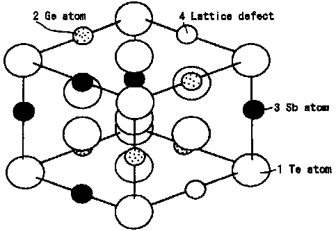
FIG. 1 is a schematic view to show a structure (atom position at a time
of crystallization) of a representative recording film used for an information
recording medium of the present invention, in which the crystalline phase is a
single phase. In this example, the crystalline phase is constituted with a
single compound phase (moreover, it is a rock-salt type structure). In the
lattice site position forming the rock-salt type structure, all 4a sites are
occupied by Te atoms 1, while 4b sites are occupied by Ge atoms 2, Sb atoms 3,
and occupied randomly by also lattice defects 4. In the
present invention, atoms other than the atoms occupying the
4b sites are filled in the lattice defects.
FIG. 2 is a schematic view to show a structure (atom position at a time
of crystallization) of another representative recording film used for an
information recording medium of the present invention, in which the
recording layer is a complex phase (a crystalline phase). In FIG. 2, (a)
8
01-09-12 16:25 TO-SMART FROM-IKEUCHI.SATO & PARTNER PATENT ATTORNEYS T-456
P.13/5? F-935
CA 02368171 2001-09-14
denotes a crystalline phase 100. The crystalline phase is a complex phase
(mixture phase) 100 comprising a component 110 having a compound
structure basically equal to that shown in FIG. 1 and also an amorphous
component 120. In FIG. 2, (b) denotes an amorphous phase 200. In (b), a
single phase is formed.
FIGs. 3A-3D are further specific examples of the structure shown in
FIG. 2.
FIGs. 4A-4J are cross-sectional views of an example of a layer
constitution of an optical information recording medium according to the
present invention. In FIGs. 4A-4J, 7 denotes a substrate, 8 denotes a
recording layer (phase change material layer), and 9 and 10 denote protective
layers. Numeral 11 denotes a reflective layer, 12 denotes an overcoat layer,
13 denotes an adhesive layer, and 14 denotes a protective plate. Numeral 15
denotes a surface layer, 16 and 17 denote interface layers, 18 denotes an
optical absorption layer, 19 denotes a reflective layer (light incident side),
and
and 21 respectively denote multilayer films of the above-mentioned thin
films.
FIG. 5 is a schematic view of a crystal structure to show positions of
additional elements in the crystalline phase of a recording film used for an
20 information recording medium according to the present invention. Numeral
22 denotes a position of an atom filling a lattice defect in a rock-salt type
crystal lattice.
FIGs. 6A-6C are graphs to show laser modulation waveforms to
evaluate the recording performance of an optical information recording
medium according to the present invention. FIG. 6A shows the recording
performance regarding a 3T pulse, FIG. 6B shows the recording performance
regarding a 4T pulse, and FIG. 6C shows the recording performance regarding
5T-11T pulses.
FIG. 7 is a graph to show a relationship between a proper additive
concentration and a lattice defect concentration in an information recording
medium according to the present invention.
FIGs. 8A-8F and 9A-9E show examples of crystal structures of
recording films used for information recording media according to the present
invention. The respective structures will cope with any compound phases
35i shown in FTGs. 1 and 2.
FIG. 10 is a schematic view to show a basic structure of an electric
memory device (a reversible change memory of a resistor) according to the
9
73466-76 CA 02368171 2001-09-14
present invention. In FIG. 10, 23 denotes a substrate, 24 and 27 denote
electrodes, 25 denotes an insulator, 26 denotes a phase change material film,
28 and 29 denote switches, 30 denotes a pulse power source, and 31 denotes
an electrical resistance meter.
Best Mode for Carrying Out the Invention
FIG. 4 is a cross sectional view to show an example (layer constitution)
of an optical information recording medium according to the present invention.
Atypical information recording medium is constituted by forming a recording
layer 8 having the above-mentioned constitution on a substrate 7 selected
from transparent polycarbonate resin, an acrylic resin, a polyolefin-based
resin, a glass sheet or the like. Protective layers 9 and 10 can be formed on
at least one surface of the recording layer. Reflective layers 11 can be
formed
on the respective protective layers. Overcoats 12 can be formed on the top
layers, or the overcoats can be replaced by protective plates 14 that are
adhered by adhesive layers 13. For guiding laser beams used in
recording/reproducing, a spiral or concentric circular concave-convex groove
track, a pit array, a track address can be formed on the substrate surface.
Such a recording medium is irradiated with a laser beam in order to cause
reversible phase change in the recording layer between a crystalline phase
and an amorphous phase, so that information can be rewritten. In the case
of crystallization, the recording medium is irradiated with a laser beam like
a
pulse in order to keep the irradiated part at or above an interim
crystallization change temperature. In changing the recording layer to be
amorphous, the layer is irradiated with a more intensive laser beam for a
period equal to or shorter when compared to a case of crystallization, so that
the irradiated part is melted instantaneously and then quenched. This
reversible phase change can be detected as a change in the reflectance or
transmittance. This reproduction is carried out by irradiating the recording
medium with a laser beam weakened not to provide any additional influence
so as to detect changes in the strength of light reflected from the irradiated
portion or transmitted.
An optical information recording medium according to the present
invention, as shown in FIGs. 4A-4J, will be characterized by a comifosition of
a
material composing the recording layer 8 and by the internal structure. A
representative example will be explained below with reference to a Ge-Sb-Te
based material. As reported in N. Yamada et al., J. Appl. Phy.69(5), 2849
73466-76 CA 02368171 2001-09-14
(1991), a Ge-Sb-Te material is crystallized to have a face-centered cubic
structure meta-stably by irradiating a laser beam. In addition to that, a
recent research presentation by the same author (MRS-Buttetin, 21(9),
48(1996) and a research presentation by Nonaka et al. (papers for the tenth
symposium on phase change recording, p.63) suggest that the metastable
phase necessarily contains many lattice defects (vacancy). The following
description is about a representative composition of a stoichiometric
compound composition of Ge2Sb2Te5. The material has a metastable phase of
rock-salt type (NaCl type). As shown in FIG. 1, all lattice positions (4a
sites)
corresponding to Cl atoms are occupied by Te atoms 1, and all lattice site
positions (4b sites) corresponding to Na atoms are occupied by Ge atoms 2 and
Sb atoms 3 at random depending on the composition ratio. However, since
the total number of the Ge atoms and the Sb atoms is greater than the
number of the Te atoms, the 4b sites necessarily has lattice defects 4 of
about
20% (about 10% of the entire sites). The lattice defects also are located at
random (An example of atom positions in 4a sites is shown).
The inventors reported that such a Ge-Sb-Te system makes a crystal
having a substantially identical face-centered-cubic crystal structure even if
the composition is changed. Recent studies show that a Sb atom does not
enter a crystal lattice but an added Sb atom exists in a separate structure on
an interface of a crystal particle even if Sb is included in a form of, e.g.,
Ge2Sb2+xTe5 (0 < x:5 1) to fill the defects. Particularly, the Sb atom will
exist
in an amorphous phase especially for a case of laser crystallization.
Specifically, the result of observation by a detailed X-ray diffraction
demonstrates that even if Sb is added to a stoichiometric composition
Ge2Sb2Te5 thin film, the Sb atom does not enter the crystal lattice to fill
the
lattice defect completely. As a result, Ge2Sb2Te5 crystal and Sb will coexist
in
a structure of a recording film in a crystalline state. In a typical case of
two-
phase coexistent composition, repetition of a melting-solidification process
will
cause a phase separation, and this will lead to local variation in the
composition. An advantage of this case is that such a phase separation will
not proceed since the melting point of Sb is considerably close to that of Ge-
Sb-Ta and since the Ge-Sb-lb also includes Sb.
Besides Sb, some adetives can prevent crystal growth though the
conditions vary in many cases. For example, JP-A-7-214913 discloses the
addition of Pd. This reference discloses that crystallization becomes
difficult
when the amount of the additives exceeds 2 atom%. From the fact that a
11
01-09-12 16:27 TO-SMART FROM-IKEUCHI.SATO & PARTNER PATENT ATTORNEYS T-456
P.16/57 F-935
CA 02368171 2001-09-14
very small amount of additive causes an abrupt change in the characteristics,
Pd is considered to exist without entering the lattice defects. In other
words,
even a small amount of Pd is considered to be separated completely from Ge-
Sb-Te but not to enter a crystal lattice based on Ge-Sb-Te. However, when
the Pd concentration reaches about 2 atom%, characteristics of Pd as a
material having a high-melting point become remarkable, and the Pd will
restrict the movement of atoms so as to substantially prevent crystallization.
Moreover, repetition of recording and erasing accelerates phase separation of
the Ge-Sb-Te and Pd. In other words, an additive that does not enter a
lattice cannot be suitable for controlling the characteristics.
On the other hand, a relatively easy relationship between Sb
concentration and change in the crystallization characteristics facilitates
control of the characteristics and serves to maintain high repeatability. This
fact may suggest that the melting point of an additional element cannot be too
much higher than that of the base material in order to change the
characteristics widely and continuously by adding the element. It is also
desirable that the additional element can enter the crystal lattice and
especially, the element does not create a separate crystalline phase. A
further merit is that entering of excessive and harmful atoms can be
prevented by previously filling the lattice defects with useful atoms.
The inventors evaluated recording materials from the above-
mentioned aspects and found that additional elements enter crystal lattices
and thus characteristics can be controlled continuously with high accuracy
under a certain condition. The inventors found also that some additives will
take place of elements of the base material. Moreover, the additives may
change the purged elements. In addition, the temperature and speed of
crystallization can be controlled by controlling the condition and
concentration
of the purged elements, and this will lead to desirable recording/erasing
performance. It is reasonable that in this case, a part of elements forming a
compound in a crystal is common to elements that have been purged outside
the compound and exist in an amorphous phase in the grain boundary or the
like. This means that positional uniformity of the composition will be
maintained easily all the time that phase changes between a crystalline phase
and an amorphous phase occur. Specifically, the additives prevent the
progress of phase separation even when the crystalline phase becomes a
complex phase, and thus, good repeatability can be maintained. It can be
concluded from the above facts that a material being a single phase and
12
01-09-12 16:28 TO-SMART FROM-IKEUCHI.SATO & PARTNER PATENT ATTORNEYS T-456
P.17/57 F-935
CA 02368171 2001-09-14
necessarily including lattice defects can provide unexpected characteristics
by
filling the lattice defects appropriately with any other atoms. Also, it is
suggested that addition of a certain element can help formation of a material
having a new structure.
The following explanation is about a specific material composition to
constitute a recording layer 8. A primary condition for a material in the
present invention is to obtain a material comprising many lattice defects. A
crystalline phase comprising lattice defects will appear as a metastable phase
in materials that can be represented by GeTe-M2Te3 (M is, for example, Sb, Bi
or Al). The examples are a Ge-Sb-Te based material comprising a GeTe-
Sb2Te3 composition, a Ge-Bi-Te material comprising a GeTe-Bi3Te3 based
composition, or a Ge-Te-Al based material comprising a GeTs-Al2Te3 based
composition. Similarly, a crystalline phase including lattice defects will
appear as a metastable phase in compositions of the mixtures such as Ge-Sb-
Bi-lb, Ge-Sb-Al-lb, Ge-Bi-Al-Th, and Ge-Sb-Bi-Al-Te. Similar constitutions
are obtained for Ge(Te,Se)-M2(Te,Se)3 in which a part of Te is replaced by Se.
The examples are Ge-Te-Se-Sb, Ge-Te-Se-Bi, Ge-Te-Se-Sb-Bi, Ge-Te-Se-Al,
Ge-Te-Se-Sb-Al, Ge-Te-Se-Bi-Al, and Ge-Te-Se-Sb-Bi-Al. Similar effects were
obtained by applying, for example, Ge-Sn-Te-Sb, Ge-Sn-Te-Sb-Al, Ge-Pb-Te-Sb,
and Ge-Pb-Te-Sb-Al, which are obtained by substituting a part of the Ge with
Sn or with Pb. Similar constitutions were obtained when N was added to the
compositions. These are crystallized meta-stably to have a face-centered-
cubic crystal structure (rock-salt structure). When the 4b sites of the rock-
salt type structure are occupied by Te (or Se) and the 4a sites are occupied
by
other element M as mentioned above, Te (or Se) atoms outnumber M atoms,
which will create lattice defects at the 4a sites inevitably. The lattice
defects
cannot be filled completely with the above-mentioned elements such as Sb.
The reason has not been clarified yet, but it can be deduced that a metastable
phase of a rock-salt type cannot be formed without a certain number of lattice
defects inside thereof. Namely, filling the defects may raise the entire
energy
so that the rock-salt type structure cannot be kept.
As a result of various analyses and experiments, the inventors have
found that not all elements can fill lattice defects and that an ionic radius
is
an important factor to determine the conditions. When the 4a sites have
lattice defects, the defected lattices of the base materials will be filled
easily if
Rim is sufficiently close to Rnc, where Rnc denotes an ionic radius of an
element having a minimum ionic radius among elements occupying the 4a
13
73466-76 CA 02368171 2001-09-14
sites and Rim denotes an ionic radius of an additional
element. According to Third Revision of Manual of Basic
Chemistry (Kagaku-binran Kiso-hen) II issued by Maruzen Co.,
Ltd., the radius of a Ge4+ ion is 0.67nm, the radius of a Sb5+
ion is 0.74nm, and the radius of a Tee- ion is 2.07nm when
the coordination number is 6. For Ge-Sb-Te, an element can
enter a lattice easily when it has an ionic radius
substantially the same or slightly smaller than the radius
of a Ge ion located at a 4b site. Each Ge ion has a smaller
ionic radius than that of a Sb ion.
14
01-09-12 16:30 TO-SMART FROM-IKEUCHI.SATO & PARTNER PATENT ATTORNEYS T-456
P.19/57 F-935
CA 02368171 2001-09-14 _
Table 1
Ionic radii and element's melting points for respective ion species
tut Xxxies Ion yxci..,s
Eiertteni s ElemcMU's
No, with a with a Ionic tudius
Ionic radius [Welting point NO, rttclting point
cootdituttian coordination
numberof6 (n0) ('C) of6 (no) ("C)
1 N 2.7 -209.86 41 Ta 7.8 2990
2 V5+ 5.0 1890 42 Mn3+h 7.9 1240
3 S + 5. 1 112.8 43 Ca + 7.9 1490
4 Si + 5.4 1410 44 Fe + 7.9 1540
P 5.8 44.1 45 Tc 7.9 2170
6 Be + 5.9 1280 46 ko + 7.9 2620
7 As + 6.0 817 47 14+ 8.0 3400
8 Se + 6.4 217 48 Hn 8.1 1240
9 Ge + 6.7 937.4 49 TO + 8.1 1660
11n + 6.7 1240 50 Rh 3+ 8. 1 1970
11 Re 6.7 3180 51 Ru 8.2 2310
12 Al 6.8 660.37 52 Ir + 8.2 2410
13 C03+1 6.9 1490 53 Nb + 8.2 2470
14 F63+1 6.9 1540 54 Ta + 8.2 2990
Cr 6.9 1860 55 Sn 8.3 231.96
16 Re + 6.9 3180 56 Ni + 8.3 1450
17 Te 7.0 449.5 57 N 8.3 2620
18 Ni3+1 7.0 1450 58 Hf + 8.5 2230
19 Aa 7.2 817 59 Rg 8.6 648.8
_ 10+1 7.2 1240 60 Zr 8.6 1850
21 Y 7.2 1890 61 Nbd+ 8.6 2470
22 Yo 7.3 2620 62 Ta + 8.6 2990
23 S + 7.4 630. 74 63 Ge + 8.7 937.4
24 Ni + 7.4 1450 64 Cu + 8.7 1083.4
Rh 7.4 1970 65 U 8.7 1132.3
26 It+ 7.4 3400 66 Crz+l 8.7 1860
27 Co 7.5 1490 67 Zn + 8.8 419.58
28 Fe 7.5 1540 68 Sc 8.8 1540
29 Ti + 7.5 1660 69 Co + 8.9 1490
Yo 7.5 2620 70 Li 9.0 180.54
31 GO + 7.6 29. 78 71 Bi + 9.0 271. 3
32 Pd 7.6 1550 72 S 9.0 630.74
33 C r3+ 7.6 1860 73 Pd 3+ 9.0 1550
34 RU 4+ 7.6 2310 74 Cu 9.1 1083.4
15+ 7.6 3400 75 Pb 9.2 327.502
36 pt 4+ 7.7 1770 76 Fe + 9.2 1540
37 Ir + 7.7 2410 77 V2+ 9.3 1890
38 Os + 7.7 3045 78 In 9.4 156.61
39 VUT_ 7.8 1890 79 pt z+ 9.4 1770
Nb 7.8 2470 80 -Crz+11 9.4 1860
CA 02368171 2001-09-14
73466-76
Atoms in a rock-salt structure are considered to have a coordination
number of 6. Table 1 is a list of ion species each having a coordination
number of 6 and ionic radius of about 0.67 nm in an order of the ionic radius.
Since a Ge' ion has ionic radius of 0.67 nm, ions ranging from a vanadium ion
Vs'
that is about 70% of a Ge`+ ion to a Ni' ion that is about 105% may enter a
lattice. That is, effective elements are V, S, Si, P, Be, As, Se, Ge, Mn, Re,
Al,
Co, 'Ile, Cr, and Ni. Among them, V, S, Si, Mn, Al, Co, Cr, and Ni etc. are
suitable. The remaining elements are not suitable, since, for example, Be, As
and P may cause problems due to the toxicity, while Ge and Te compose the
base material, and Re is a radioactive element.
Elements for filling lattices are not limited to the above-mentioned
ones. The above-mentioned condition is just one factor to determine easy
access to a lattice. An element that composes a compound of a rock-salt type
structure is observed to enter a lattice easily. Specifically, Ag, Sn and Pb
were observed entering lattices, since Ag, Sn and Pb compose AgSbTe21 SnTh,
and PbTe respectively.
In addition to the suitability to fill a lattice, another important factor
for additional elements is the melting point. Formation of an amorphous
mark with a phase change optical disk requires a process of melting a
recording film before quenching. For such a case, a melting point of the
additive is preferred to be close to the melting point of an entire recording
film
(more preferably, a melting point of the additive is close to melting points
of all
elements composing the recording film). If the additive has a melting point
much higher than the entire melting point, phase separation will proceed
easily during repetition of melting and solidification. In such a case, it is
difficult to keep the additives stably in lattices even when the ionic radii
are
closer to each other. In other words, phase separation occurs, and the phase
separation creates a region comprising more additives and a region
comprising fewer additives. It is preferable to decrease the difference
between the melting points, however, when the difference is about 100 C,
lattice defects can be filled while creating substantially no phase
separation.
Otherwise an extremely uniform mixed phase can be formed even without
forming a single phase. For a case of Ge2Sb2Th,, the melting point is about
630 C. Therefore, an additive is preferred to have a melting point in a range
from about 530 C to 730 C. Table 2 is a list of elements to form ions having
coordination number of 6 as mentioned above, and the elements are described
sequentially from the one with a lower melting point. This table shows that
16
01-09-12 16:32 TO-SMART FROM-IKEUCHI.SATO & PARTNER PATENT ATTORNEYS T-456
P.21/57 F-935
CA 02368171 2001-09-14
elements ranging from No. 25 (Sb) to No. 31 (Ba) are within the range. That
is, corresponding elements are Sb, Pu, Mg, Al and Ba, from which Pu as a
radioactive element and Sb as a base material are excluded. The remaining
Mg, Al, Ba or the like are used suitably for the purpose.
17
01-09-12 16:32 TO-SMART FROM-IKEUCHI.SATO & PARTNER PATENT ATTORNEYS T-456
P.22/57 F-935
CA 02368171 2001-09-14 _
Table 2
Melting points of respective elements and ionic radii of ion species
Ion species
ion sp ith Ionic radius Ei mcnt a ; cles Ionic rndiiu Elcmunt s
No. coutfunmion melting point NO. Cootdinwinn melting point
number (nm) ('C) number ' (nla) ( C)
1 Cs+ 18.1 28.4 41 Ge + 8.7 937.4
2 Ga * 7.6 29. 78 42 Ge + 6.7 937.4
3 Rb+ 16.6 38.89 43 AB+ 12.9 961.93
4 p3+ 5.8 44.1 44 AB + 10.8 961.93
K+ 15.2 63.65 45 Nd + 11.2 1020
6 Na 11.6 97.81 46 Ac 12.6 1050
7 S Z- 17.0 112.8 47 Au 15.1 1064.43
8 S 5.1 112.8 48 Cu 9.1 1083.4
9 I- 20.6 113.5 49 _CUT__ 8.7 1083.4
In + 9.4 156.61 50 U + 11.7 1132.3
11 Li+ 9.0 180.54 51 U 10.3 1132.3
12 Se Z- 18.4 217 52 + 8.7 1132.3
13 Se 4+ 6.4 217 53 In + 8.1 1240
14 Sn + 8.3 231.96 54 Un + 9.7 1240
Bi 11.7 271.3 55 Iln 7.2 1240
16 Bi + 9.0 271.3 56 Y 7.9 1240
17 Tl 16.4 303.5 57 to 6.7 1240
18 T13+ 10.3 303.5 58 Be 2+ 5.9 1280
19 Cd 10.9 320.9 59 Gd 10.8 1310
Pb + 13.3 327.502 60 10.5 1410
21 Pb + 9.2 327.502 61 Si 5.4 1410
22 Zn 8.8 419.58 62 Ni 8.3 1450
23 Te - 20.7 449.5 63 Ni + 7.0 1450
24 TO + 7.0 449.5 64 Ni + 7.4 1450
Sb 9.0 630. 74 65 C02+1 7.9 1490
26 Sb + 7.4 630. 74 66 + 8.9 1490
27 Pu + 11.4 639.5 67 Co + 6.9 1490
28 Pu + 10.0 639.5 68 Co 7.5 1490
29 vg z+ 8.6 648.8 69 Y 10.4 1520
A1 3t 6.8 660.37 70 Sc 8.8 1540
31 Ba + 14.9 725 71 Fe2+1 7.5 1540
32 Sr + 13.2 769 72 Feztn 9.2 1540
33 Ce 3+ 11.5 799 73 Fe 6.9 1540
34 Ce + 10.9 799 74 Fed+n 7.9 1540
As 7.2 817 75 Pd 10.0 1550
36 As + 6.0 817 76 Pd + 9.0 1550
37 Eu + 13.1 822 77 Pd 7.6 1550
38 Eu 10.9 822 78 Lu 10.0 1660
39 Ca + 11.4 839 79 Ti 10.0 1660
La 11. T 921 80 Ti 8. 1 1660
18
01-09-12 16:33 TO-SMART FROM-IKEUCHI.SATO & PARTNER PATENT ATTORNEYS T-456
P.23/57 F-935
CA 02368171 2001-09-14 _
For example, when the base material comprises a Ge2Sb2Te5
composition, Al is a suitable element that can satisfy the two conditions
concerning ion radius and melting point simultaneously, while it is free of
toxicity or radioactivity. A GeTe-Sb2Te8-based composition can be treated in
the same manner as Ge2Sb2Te5. While the melting point of the GeTh-Sb2Te9-
based composition changes continuously in a range from 593 C to 725 C, Al
was effective as well in filling lattice defects. Similarly, in any material
compositions based on Ge and Te, Al was effective in filling lattice defects.
Needless to say, elements other than Al were confirmed to enter lattices. It
was confirmed that Ag, Cr, Mn, Sn, Pb, Mo In and Se enter lattices.
Elements to fill lattice defects are not limited to one kind, but plural
kinds of elements can be filled simultaneously. In an experiment performed
by the inventors, the crystallization speed was improved remarkably by, for
example, filling Sn (or Pb) in lattices when the material is Ge-Sb-Te based
material or Ge-Bi-Te based material. The repeatability was improved by
filling Cr in lattices. Therefore, the crystallization speed and repeatability
were improved at the same time by filling Sn (or Pb) together with Cr.
Similar effects were obtained by filling Mn in place of Cr in the crystal
lattices.
Filling Ag was helpful in improving optical reflectance variation between a
crystalline phase and an amorphous phase (improvement in recording signal
amplitude). Therefore, improvement in the recording signal amplitude and
the crystallization speed was achieved simultaneously by adding Ag and Sn
(or Pb) together. Signal amplitude and repeatability were improved
simultaneously by filling Ag and Cr (or Mn) at the same time. The addition
of Sn (or Pb), Ag and Cr (or Mn) together served to improve crystallization
speed, signal amplitude and repeatability simultaneously.
FIG. 2 indicates a preferred embodiment for a recording layer used for
another optical information recording medium according to the present
invention. FIG. 2 expresses schematically a partial microscopic structure of
a recording layer 8 at a laser irradiation part in any of FIGs. 4A-41. In FIG.
2,
(a) denotes a crystalline phase (complex phase) 100 comprising a mixture of a
compound component 110 and an amorphous component 120, while (b)
denotes a single-amorphous phase 200. The recording material layer is
composed of the four elements of Ge, Sb, Te and Sn. The crystal component
110 in the complex phase 100 has a NaC1 type structure comprising the four
elements of Ge-Sb-Te-Sn. The 4a sites of the NaCl type structure (sites
corresponding to Cl) are occupied by Te, while the 4b sites (sites
corresponding
19
01-09-12 16:34 TO-SMART FROM-IKEUCHI.SATO & PARTNER PATENT ATTORNEYS T-456
P.24/57 F-935
CA 02368171 2001-09-14 _
to Na) are occupied randomly by Ge, Sb and Sn. At the 4b sites there are
lattice defects to accept no atoms, which tends to decrease entire density. As
a result, volume variation between the crystalline phase and amorphous
phase is decreased, and inconvenience such as deformation or perforation
caused by the phase change is prevented. In the grain boundary,
components that cannot enter the lattices exist in an amorphous state. Here,
Sb exists in an amorphous state. It is preferable that an amount of the
amorphous component is twice or less than the crystal component by number
of molecules. It is preferable A/C < 2, or more preferably, A/C :5 1, where C
denotes a number of molecules of the crystal component and A denotes a
number of molecules of the amorphous component. When the ratio of the
amorphous component exceeds twice, the crystallization speed will be lowered
remarkably. On the other hand, when the ratio is close to 0, the
crystallization speed is increased excessively. It is preferable that A/C >
0.01.
The element that is found as an amorphous component in the crystalline
phase is not limited to Sb but it can be Ge. Ge is effective in raising
crystallization temperature or improving repeatability. The great viscosity of
the amorphous Ge is considered to provide such effects. It has been
confirmed that elements such as Mn and Cr can be added for depositing Ge.
From a macroscopic viewpoint, all elements are arranged in a
substantially uniform state in the single-amorphous phase 200. It is
important for the recording film to change reversibly between the two states
during recording or rewriting information. At this time, it is preferable that
a part of the elements for forming the amorphous phase 120 and elements for
forming the compound component 110 in the complex phase 100 is common, so
that the distance of atomic diffusion is decreased at the time of phase change
so as to complete the change rapidly. It is effective also in preventing
generation of great positional compositional segregation when rewriting is
repeated many times.
A material layer composing the recording layer comprises a material
for forming a crystalline phase in a complex phase, and the material is
represented by a format of Ma-Mb-Mc-a, in which Ma comprises Ge and at
least one of Sn and Pb, Mb comprises at least one of Sb and Bi, and Mc
comprises at least one of Te and Se. Any other elements can be added if
required. For example, Mn, Cr, Ag, Al, In or the like can be added. For a
material for forming an amorphous phase in the complex phase, Sb or Ge is
suitable for a Ge-Sb-Te based material, while Ge or Bi is suitable for a Ge-Bi-
73466-76 CA 02368171 2001-09-14
Te based material. For a AgInSbTe based material, In can be used.
In general, protective layers 9 and 10 in FIGs. 4B-41 are made of a
dielectric material. Protective layers suggested as optical disk media in
conventional techniques can be used as well. The examples include a
material layer of an oxide alone or a complex oxide of an element selected
from
Al, Mg, Si, Nb, Ta, Ti, Zr, Y, and Ge; a material layer of a nitride or a
nitride-
oxide of an element selected from Al, B, Nb, Si, Ge, Ta, Ti, and Zr; a sulfide
such as ZnS and PbS; a selenide such as ZnSe; a carbide such as SiC; a
fluoride such as CaF2 and LaF; and a mixture thereof such as ZnS-SiO3 and
ZnSe-SiO2.
A reflecting layer 11 is based on a metal such as Au, Al, Ag, Cu, Ni, Cr,
Pd, Pt, Si, and Ge, or an alloy such as Au-Cr, Ni-Cr, Al-Cr, Al-Ta, Al-Ti, Ag-
Pd,
Ag-Pd-Cu, Si-W, and Si-Ta.
An overcoat layer 12 can be made of, for example, a photo-curable
16 resin. An adhesive 13 can be made of, for example, a hot-melt adhesive or a
photo-curable resin such as an ultraviolet curable resin. A protective plate
14 can be made of the same material as the substrate. The substrate is not
transparent necessarily for a constitution to record and reproduce by
irradiating a laser beam from the side having a recording layer. The above-
mentioned substrate can be replaced by, for example, a plate of a light metal
such as Al and Cu, or a plate of alloy based on the light metal, and a plate
of
ceramics such as A1203 and MgO,. In this case, the respective layers are
formed on the substrate in a reversed order.
Though it is not indispensable, a surface layer 15 can be provided on
the outermost in order to prevent damage caused by a contact with an optical
head. The surface layer can be made of a lubricant material comprising e.g.,
a diamond-like-carbon and a polymer material.
Interface layers 16 and 17 can be formed in an interface between the
recording layer and at least one of the protective layers for several
purposes,
such as preventing atomic diffusion in spacing between the recording layer
and the protective layer. Especially, nitrides, nitride-oxides and carbides
are
suitable for the interface layer. The examples include materials of Ge-N-(O),
Al-N-(O), Si-C-N, Si-C or the like, and materials further including Cr, Al or
the
like, such as Ge-C-N and S i - Al . Optical absorption Aa of a recording layer
ip
an amorphous state can be decreased relatively with respect to optical
absorption Ac of the recording layer in a crystalline state by applying an
optical absorption layer 18 over an upper protective layer of the recording
21
01-09-12 16:36 TO-SMART FROM-IKEUCHI.SATO I PARTNER PATENT ATTORNEYS T-456
P.26/57 F-935
CA 02368171 2001-09-14
layer, or by applying a semitransparent reflecting layer 19 at the light
incident side of the recording layer.
The optical absorption layer can be made of alloy materials based on
Si and Ge, or alloy materials based on To. The reflecting layer can be made of
the same material, or it can be formed by laminating dielectric films having
different refractive indices, such as Si02/ZnS-Si02/Si02. An alternative
medium can have both surfaces made by adhering a recording medium having
these multilayer films 20 and 21 through adhesive layers 13.
A multilayer film used for an optical information recording medium
according to the present invention can be formed by an ordinary method for
forming a thin film. The method is selected, for example, from magnetron
sputtering, DC sputtering, electron beam deposition, resistance heating
deposition, CVD, and ion plating. Especially, magnetron sputtering using an
alloy target, and also DC sputtering are excellent in obtaining uniform films
that will be used as recording films in the present invention. A target used
for sputtering contains a main component of a material for forming the above-
mentioned rock-salt structure, to which an element for filling the lattice
defects is added. Such a target can be prepared by solidifying powders
composed of respective elements at a proper ratio, and the elements are, for
example, Ge, Te, Sb and Al; Ge, Sb, Sn, Cr and Te; Ge, Sb, To, Sn andAg.
Though the component ratio in the target substantially corresponds to
compositions of the recording film, minor adjustment for every apparatus is
required since the components will be influenced by the apparatus. For
example, Dad is equal substantially to Dim _5 Ddf x 1.5, where Dim denotes a
concentration of an additive in a film of the crystalline phase, Ddf denotes a
concentration of lattice defects, and Dad denotes a concentration of an
additive in a target. In general, an amorphous single phase is formed just
after film formation, which will be transformed into a crystalline phase
(initialization). It is possible to form a phase as a mixture of the
crystalline
phase and the amorphous phase by irradiating with a high density energy flux.
In irradiation of the high density energy flux, it is desirable to penetrate
the
flux at a high temperature for a short period. Therefore, laser irradiation
and flash irradiation are used suitably.
FIG. 10 is a schematic view to show a basic structure of an electric
memory device according to the present invention (a reversible change
memory of a resistor). In FIG. 10, 23 is a substrate selected from a glass
sheet, a ceramic sheet such as Als09, and sheets of various metals such as Si
22
01-09-12 16:36 TO-SMART FROM-IKEUCHI.SATO & PARTNER PATENT ATTORNEYS T-456
P.27/57 F-935
CA 02368171 2001-09-14
and Cu. The following explanation is about a case for using an alumina
substrate. In FIG. 10, an Au layer is sputtered to provide an electrode 24 on
a substrate. Subsequently, a layer 25 of an insulator such as SiO2 or SiN is
formed thereon through a metal mask, and further, a recording layer 26
comprising a phase change material similar to the above-mentioned recording
layer for the optical information recording medium, and also an electrode (Au)
27 are laminated. Between the electrodes 24 and 27, a pulse power source 30
is connected through a switch 28. For crystallizing the recording film that is
in highly resistant under as-depo.-condition in order to change into a low
resistant state, the switch 28 closes (switch 29 open) so as to apply voltage
between the electrodes. The resistance value can be detected with a
resistance meter 31 while opening the switch 28 and closing the switch 29.
For reversely transforming from the low resistant state to a high resistant
state, voltage higher than the voltage at the time of crystallization is
applied
for the same or shorter period of time. The resistance value can be detected
with a resistance meter 31 while opening the switch 28 and closing the switch
29. A large capacity memory can be constituted by arranging a large number
of the memory devices in a matrix.
The present invention will be described further by referring to specific
examples.
(Example 1)
Example 1 is directed to a method for manufacturing an optical
information recording medium according to the present invention. A
substrate used in this example was a disc-shape polycarbonate resin substrate
that was 0.6mm in thickness, 120mm in diameter and 15mm in inner
diameter. A spiral groove was formed substantially on the whole surface of
the substrate. The track was a concave-convex groove having a depth of
70nm. Both the groove portion and the land portion of the track had a width
of 0.74 m. A multilayer film would be formed on the surface later. A laser
beam for recording/reproducing an information signal can move to an
arbitrary position on the disk by a servo signal provided from the concave-
convex shape. On the substrate, the following layers were formed in this
order: a ZnS:20 mol% Si02 protective layer 150nm in thickness; a
Ge2Sb2Th5Ala,g thin film 20nm in thickness; a GeN interface layer 5nm in
thickness; a ZnS:20 mol% Si02 protective layer 40nm in thickness; and an
A197Cr3 alloy reflecting plate 60nm in thickness. The protective layers were
prepared by magnetron sputtering using a ZnS-Si02 sintered target and Ar
23
01-09-12 16:38 TO-SMART FROM-IKEUCHI.SATO & PARTNER PATENT ATTORNEYS T-456
P.28/57 F-935
CA 02368171 2001-09-14 _
sputtering gas. The recording layer and the reflecting layer were prepared
by DC sputtering in which respective alloy targets and Ar sputtering gas were
used. The interface layer was formed by a reactive magnetron sputtering
using a Ge target and a sputtering gas as a mixture of Ar gas and N2 gas. In
any cases, N2 gas can be added to a sputtering gas. After completing the film
formation, an ultraviolet curable resin was spin-coated, and a polycarbonate
plate the same as a substrate was adhered to serve as a protective plate, and
this was irradiated by a ultraviolet beam lamp subsequently for curing, before
subjecting the disk to an initial crystallization by irradiating a laser beam.
The thus obtained optical information recording medium can record and
reproduce by means of laser irradiation. In an inspection with an X-ray
diffraction, the part that was subjected to the initial crystallization was a
NaCl type single-crystalline phase having Al in the crystal lattices, though a
slight halo peak was observed. The same inspection was carried out for the
other additive elements, and similar results were observed for Mn, Ag, Cr, Sn,
Bi, and Pb.
(Example 2)
On a quartz substrate, eight kinds of thin film material were formed
by DC sputtering. The materials were represented by Ge2Sb2Te5A] , in which
Al:x = 0.0, A2:x = 0.2, A3:x = 0.5, A4:x = 1.0, A5:x = 1.5, A6:x = 2.0, A7:x =
2.5,
and A8:x = 3Ø The base vacuum degree was 1.33 x 10'4Pa, and Ar was
introduced to make the vacuum degree to be 1.33 x 10.1 Pa. Under this
condition, 100W power was applied between a cathode and an alloy target of
100mm1D in diameter so as to form a thin film having a thickness of 20nm.
These samples were monitored by using a He-Ne laser beam in the varying
strength of the transmitted light while being heated at a programming rate of
50 C/minute in order to measure a temperature at which transmittance was
decreased remarkably as a result of crystallization. The results are shown in
Table 3.
Table 3
Relationship between Al concentration in a Ge2Sb2` e5 thin film
and crystallization temperature = crystallization speed
Sample Al A2 A3 A4 AS A6 A7 AS
Al con. 0% 2.2% 5.3% 10% 14.3% 18.2% 21.7% 25%
T. 180 C 183 C 189 C 200 C 227 C 255 C 305 C 350 C
T, o 0 0 0 o x X
24
CA 02368171 2001-09-14
73466-76
The increase of the crystallization temperature becomes sharp when
the Al concentration is at a level of the sample A5 . For this composition,
Ddf
(concentration of lattice defects) occupies 10% of the whole sites (20% of the
4b
sites). For the respective samples, ratios that Al atoms fill lattice defects
to
Ddf are as follows: A1:0, A2:0.2 x Ddf, A3:0.5 x Ddf, A4:1.0 x Ddf, A5:1.5 x
Ddf,
A6:2.0 x Ddf, A7:2.5 x Ddf, and A8:3.0 x Ddf. For the samples A5-A8, there
are more Al atoms than the lattice defects to be filled. Percentage of the Al
atoms to the whole compositions in the respective samples are as follows. Al:
0%, A2: 2.2%, A3: 5.3%, A4: 10%, A5: 14.3%, A6: 18.2%, A7: 21.7%, and A8:
25%.
Regarding the samples A3 and A4, a Rietveld method was performed
to identify the structures in detail by using an X-ray diffractometry so as to
confirm that Al entered the crystal sites in any of the samples. FIG. 5 is a
schematic view to show such a sample. The probability that the lattice
defects are filled with the additives is determined randomly as well. For the
samples A5, A6, A7 and A8, excessive atoms that cannot enter the crystal
lattices will exist among the crystal particles. Such excessive atoms are not
always Al, but other elements such as Sb or Ge may deposit as a result of
substitution with Al. Laser irradiation period for causing crystallization
would be extended when the Al concentration is increased. In the Table, 00
indicates that crystallization occurred within 70ns, 0 indicates that
crystallization occurred within 100ns, ZS, indicates that crystallization
occurred within 200ns, and x indicates that crystallization required more
than 200ns. When an effective optical spot length is represented by 1/e2, an
ideal value would be about 0.95 m since an optical system used for the
current DVD-RAM has a wavelength of 660nm, and NA of an objective lens is
0.6. It takes about 160ns for the laser spot to traverse a disk rotating at a
linear velocity of 6m/s, which corresponds to a velocity for DVD-RAM.
Therefore, a disk with a 0 mark can be applied to a current DVD-RAM
system. It can be applied to a system having a linear velocity of at least
9m/s
as well. A disk with mark can cope with an even higher linear velocity of
at least 12m/s.
(Example 3)
Eight optical disks from al to a8 were prepared by using the
compositions of Example 2 in the method of Example 1. These disk media
were rotated at a linear velocity of 9m/s, and light beams having a wavelength
of 660nm emitted from a laser diode were focused on the disks by using an
01-09-12 16:39 TO-SMART FROM-IKEUCHI.SATO & PARTNER PATENT ATTORNEYS T-456
P.30/57 F-935
CA 02368171 2001-09-14
optical system comprising an object lens having NA of 0.6. At this time, as
shown in FIGS. 6A-6C, overwriting recording was carried out in a 8-16
modulation (bit length: 0.3 m) by applying a multi-pulse waveform
corresponding to waveforms of signals ranging from a 3T signal to a 11T
signal. The peak power and bias power were determined as follows. First, a
power to provide an amplitude of -3dB to a saturation value of the amplitude
was obtained and the power was multiplied by 1.3 to provide a peak power.
Next, the peak power was fixed while the bias power was determined to be
variable for conducting 3T recording. 11T recording was conducted with the
same power for measuring a damping ratio of the 3T signal, which was
established as an erasing rate. Since the erasing rate was increased
gradually, experienced a substantially flat region and turned into decrease,
the bias power was determined to be a central value of the upper limit power
and a lower limit power with an erasing rate of more than 20dB.
Table 4 shows recording power (peak power / bias power) at a time of
land recording for each disk, C/N, a maximum value for elimination rate, and
a number of times that a jitter value is 13% or less when random signals are
overwrite-recorded repeatedly.
Table 4
Relationship between Al concentration in Ge2Sbslle5 thin film and disk
performance
Disk al a2 a3 A4 a5 a6 a7 88
Al con. 0% 2.2% 5.3% 10% 14.3% 18.2% 21.7% 25%
Power 10.5/4.5 10.5/4.5 10.5/4.5 10.5/4.5 10.1/4.6 10.0/4.9 MW MW MW MW MW MW
MW
" N 50dB 51.5dB 52dB 52.5dB 52.5dB 52.5dB 52.OdB
Erasing 25dB 30dB 34dB 35dB 29dB 21dB 10dB ----
rate
NT 3x10' 1x10' >1x101 >I X101 1x10' 2x10 ---- ----
1): Al concentration 5~): Number of times
The results show that addition of Al improves erasing rate and
increases a number of repetitions. When the Al concentration was not higher
than a concentration (10%) of the lattice defects, erasing rates exceeded 30dB
and the repetition numbers exceeded 100,000 for any of the disks a2, a3, and
a4. It was found that optimum values were obtained for C/N, erasing rate
and repetition number when the Al concentration matches the concentration
Ddf of the lattice defects. High-speed crystallization performance was
maintained up to the time that the Al concentration became 1.5 times of the
lattice defect concentration. For the disk a5, the repetition number was
26
01-09-12 16:40 TO-SMART FROM-IKEUCHI.SATO & PARTNER PATENT ATTORNEYS T-456
P.31/57 F-935
CA 02368171 2001-09-14
increased when compared to a disk including no additives. When the
additive concentration is increased excessively, the crystallization velocity
is
lowered and thus, the erasing rate is decreased and the jitter becomes large.
For the disks a7 and a8, the jitter was over 13% from the initial stage. It
was
observed for these disks having improved repeatability that mass transfer
was restrained.
(Example 4)
Various disks were manufactured by determining the composition of
the recording film in Example 1 to be (GeTe)x(Sb2Te8)1-x, where the x value
was
varied in a range from 0 to 1. For every disk, D1 and D2 were measured. D1
denotes a proper range of Al concentration, and D2 denotes an optimum range
among D1. The concentration was determined first to be 0.2% and 0.5%, and
subsequently, it was increased by 0.5%, i.e., 1%, 1.5%, 2%, 2.5%... The
proper range was determined to be a concentration range to provide a
repetition number larger than that of a disk including no additives, and the
determination was based on the methods described in Examples 2 and 3.
The optimum range was a concentration range in which the repetition
number was doubled at least when compared to a disk including no additives
and a range that a high crystallization velocity was obtainable. Namely, it is
a range to allow crystallization by irradiating a laser beam for 150ns at
most.
Table 5
Optimum Al addition concentration for (GeTs)x(Sb2Te8)1_x
X value Ddf for NaC1 structure Al concentration within Al concentration within
Notes
__proper ran e:D 1 optimum ran :D I
0 16.7% Soje, itself
0.1 16.1% 0.20/aSD1 24.O% 3.0 / 516.0%
0.2 15.4% 0.2 / 1523.0% 3.0% 5_15.0%
0.33 14.3% 0.2%<-DI222.0% 3.0% D2_<14.0% GeSb T
0.5 12.5% 0.294 D 15_19.5% 2. 2512.5% GeS Te
0.67 10.0% 0.2% 1:516.0% 1.5%<D2511.0% Ge2Sb2Tcs
0.8 7.1% 0.2%EDI511.5% 0.5%6D2<_ 8.5%
0.9 4.2% 0.2 15 6.5% 0.2W2-< < 4.5%
0.91 3.8% 0.29/aSD 1<_ 6.0% 0.20/eSD25 4.0%
1 0% GeTe itself
Table 5 shows the test results. The table includes also calculation
results of the concentration Ddf of lattice defects. The lattice defects are
formed inevitably in a crystal structure under a hypothetical circumstance
that these material thin films form metastable phases of a rock-salt type by
laser irradiation. As indicated in the table, the concentration Ddf of the
27
01-09-12 16:41 TO-SMART FROM-IKEUCHI.SATO & PARTNER PATENT ATTORNEYS T-456
P.32/5T F-935
CA 02368171 2001-09-14 _
lattice defects increases when a (GeTe)x(Sb2Te8)1 ic quasibinary system
composition transfers from the GeTe side to the Sb2Te3 side. On the other
hand, when the proper range of Al amount reaches a range higher than a
range for the defect concentration, the range up to about 1.5 x Ddf is
effective
in improving the characteristics.
FIG. 7 is a graph to show the relationships. The solid line denotes
Ddf, while = denotes the upper limit of the proper range and 0 denotes the
upper limit of the optimum range. The upper limit of the optimum range
substantially coincides with the Ddf value while the x value is small and Ddf
absolute value is big. However, the upper limit will be bigger than Ddf by
about 20% when the x value is increased and Ddf value is decreased. The
reason can be estimated as follows. Since a part of the Al additive is
modified
due to oxidization, nitriding or the like, a percentage for entering the
crystal
lattices is lowered, and thus, the amount of the additive should be increased.
(Example 5)
Disks of Example 4 were subjected to 10000 times of overwrite-
recording of a single frequency signal having a mark length of 0.3 m before a
measurement of the CN ratio. Subsequently, the disks were kept in a
thermostat at a temperature of 901C and humidity of 80%RH for 200 hours
and the CN ratio of the same track was measured. The results are shown in
Table 6. In the table, indicates that the initial CN ratio was at least 50dB
and a decrease in the CN ratio was at most 1dB even after a 200 hours of
acceleration test. 0 indicates that the initial CN ratio was at least 50dB and
a decrease in the CN ratio was at most 3dB after a 100 hours of acceleration
test. & indicates that the initial CN ratio was at least 50dB while the CN
ratio was decreased by at least 3dB in the acceleration test. X indicates that
problems occurred during the initial overwriting of 10000 times, e.g., the CN
ratio was decreased.
Table 6
Result of acceleration test of disks based on (Ge71e).(Sb2'i1s3)(j containing
Al
X 0 0.1 0.2 0.3.9 0.5 0.67 0.8 0.9 0.91 1
ResuIt It __ _ A 0 0 0 0 a X X
(Example 6)
A similar test was carried out by changing the composition of the
recording film of Example 4 to (GeT1e)x(Bi27bs)1 ,,. Similar results were
28
CA 02368171 2001-09-14
73466-76
obtained for the effects caused by the Al addition and the proper
concentration.
(Example 7)
A similar test was carried out by changing the composition of the
recording film of Example 4 to (GeTe)x(M2Tes)1 ,, (M: a mixture comprising Sb
and Bi at an arbitrary ratio). Similar results were obtained for the effects
caused by the Al addition and the proper concentration.
(Example 8)
Disks having films with varied N concentration were prepared by
varying partial pressures of Ar gas and N2 gas, in which the recording layers
were formed by adding 7% Al to (GeTe)o.8(Sb2Tes)02. The concentration of N in
the films was identified by using SIMS. The thus obtained disks were
subjected to recording of random signals having a bit length of 0.26 m under a
condition that the recording power was 11mW (peak power) / 5mW (bias
power) and the linear velocity was 9m/s in order to examine the overwriting
characteristics. The evaluation results are shown in Table 7.
Table 7 indicates that addition of N improves recording sensitivity.
When excessive N was added, the optical constant was reduced and C/N was
lowered. The effects became apparent when 0.5% of N was added, and the
preferable amount of N was about 5%.
Table 7
Relationship between N concentration in recording thin film and disk
performance
Disks A B C D E F G H
N con. 0% 0.1% 0.5% 1% 3% 5% 10% 20%
C/N 51.OdB 51.0dB 52.0dB 52.0dB 52.5dB 52.5dB 49.5dB 45.0dB
Power 11.5/5.0 11.4/4.9 11.1/4.6 10.8/4.4 10.5/4.1 10.0/4.0 10.0/4.2 10/4.4
mW , mW mW mW mW mW mW MW mW
N con.: N concentration
(Example 9)
Various additives other than Al were added to Ge2Sb2Zhe recording
films for the purpose of examining the recording performance of the films.
Additives were selected from elements having ion radii similar to an ionic
radius of Al, i.e., V, S, Si, P, Se, Ge, Mn, Re, Co, 7b, Cr, Ni; elements
having
melting points similar to that of Al, i.e., Sb, Pu, Mg, Ba; and elements of a
separate group, i.e., Ag, Pb, and Sn. Each additive of about 5 atom% was
added for examining the effects.
29
01-09-12 16:43 TO-SMART FROM-IKEUCHI.SATO & PARTNER PATENT ATTORNEYS T-456
P.34/57 F-935
CA 02368171 2001-09-14
Disks were manufactured in accordance with Examples 1 and 3 in
order to examine the overwriting repeatability. Even if an element had an
ion radius value similar to that of Al, the element often caused phase
separation during repetition when the melting point is far from that of Al.
For an element having a melting point similar to that of Al, degradation
occurred due to mass transfer as a result of repetition if the ion radius
value
was far apart from that of Al. When Pb or Sn was added, both the
repeatability and crystallization speed were improved, while the
crystallization temperature lowered to some degree. When Ag was added,
the signal amplitude was improved, and the repetition number was increased
slightly. In conclusion, a maximum repetition number was obtained for a
disk including an additive having an ion radius and a melting point similar to
that of Al.
(Example 10)
Various additives were added to Ge3Al2Te6 recording films for the
purpose of examining the recording performance of the films. For the
additives, Sn, Pb and Ag were selected, since these elements will form a rock-
salt type crystal structure with Te (SnTe, PbTe, AgSbTe2) in a thermally
equilibrium state. Concentrations of the respective elements were 5% and
8.5%. Disks were manufactured in accordance with Examples 1 and 3 for
examining the laser crystal portions to find s rock-salt type crystal of a
single
phase. In an examination on the overwriting repeatability, no mass transfer
occurred even after 10000 times of repetition.
FIG. 8A-8F and FIGs. 9A-9E show crystal structures for
representative examples in Examples 10 and 11. In the drawings, only some
of the structures include lattice defects, which indicates that lattice
defects
are formed depending on the compositions. Te or Se atoms occupy the 4a
sites while the other atoms and lattice defects (vacancy) occupy the 4b sites.
The atoms occupy the respective sites at random and the rate is influenced by
the composition.
(Example 11)
A recording film was formed in which Sb of Example 4 was replaced by
Al. The composition of the recording film was (GeTe)x(Al2Te$)(l_,C) (x = 0.67,
0.8). The recording film was irradiated with a laser beam so as to obtain a
metastable single phase. In an evaluation of the disk performance,
overwrite-recording at a linear velocity of 9m/s was achieved. Recording
sensitivity was increased by about 10% in disks comprising the composition
01-09-12 16:44 TO-SMART FROM-IKEUCHI.SATO & PARTNER PATENT ATTORNEYS T-456
P.35/57 F-935
CA 02368171 2001-09-14
together with 3 atom% of Sb or Bi.
(Example 12)
In accordance with Example 1, various (100 kinds) optical disks were
manufactured in which the composition is represented by
[(Ge + Sn)4Sb2Te7J(loo.,,)Cr,,. In the composition, x indicates a percentage
of Sn
in the entire composition and y indicates atom%. The values of x and y were
varied in the following range:
x=0,1,2,3,4,5,8,10,15,20%
y = 0, 1, 2, 3, 4, 5, 8, 10, 15, 20%.
A substrate used in this example is a disc-shape polycarbonate resin substrate
that is 0.6mm in thickness, 120mm in diameter and 15mm in inner diameter.
A spiral groove was formed on substantially the whole surface of the
substrate.
The track was a concave-convex groove having a depth of 70nm. Both the
groove portion and the land portion of the track had a width of 0.615 m. A
multilayer film would be formed on the surface. A laser beam for
recording/reproducing an information signal can move to an arbitrary position
on the disk by a servo signal obtained from the concave-convex shape. On
the substrate, the following layers were formed in this order: a ZnS:20 mol%
Si02 protective layer 100nm in thickness; a GeN-based interface layer 5nm in
thickness; a recording layer 9nm in thickness having the above-identified
composition; a GeN interface layer 5nm in thickness; a ZnS:20 mol% SiO2
protective layer 40nm in thickness; a Ge-based or Si-based alloy layer 40nm in
thickness; and an Ag-based metal reflecting layer 80nm in thickness. The
disk characteristics were evaluated on three criteria, i.e., signal volume,
26 repetition number, and stability of rewriting sensitivity (after an
environmental test at 80 C, 90%RH for 20011). In an evaluation carried out
by taking a disk of y = 0 and z = 0 as a standard, the crystallization speed
was
increased with an increase of Sn concentration, while excessive Sn decreased
stability of an amorphous state. When Cr concentration was increased, the
crystallization speed and signal amplitude were lowered and rewriting
sensitivity was lowered due to an environmental test, while the stability of
the
amorphous state and repetition number were increased. It was confirmed
that equivalent or better performance was obtainable for all the three
criteria
when the Sn concentration was in a range from 3% to 16% and the Cr
concentration was in a range from 1% to 10%. It was effective especially in
improving both the repetition number and the stability of rewiring sensitivity
when the Sn concentration was in a range from 5% to 10% and the Cr
31
CA 02368171 2001-09-14
73466-76
concentration was in a range from 1% to 5%.
(Example 13)
In accordance with Example 12, 100 kinds of optical disks were
manufactured in which the composition is represented by
[(Ge + Sn)4Sb2Te7](1..,Agz. In the composition, x indicates a percentage of Sn
in the entire composition and z indicates atom%. The values of x and z were
varied in the following range:
x = 0, 1, 2, 3, 4, 5, 8, 10, 15, 20%
z = 0, 1, 2, 3, 4, 5, 8, 10, 15, 20%.
The thickness of the respective layers and evaluation criteria are identical
to
those of Example 12. It was confirmed that crystallization speed was raised
with an increase of Sn concentration, but stability of an amorphous state
deteriorated when the concentration was increased excessively. It was
confirmed also that increase of Ag concentration increased signal size, though
excessive Ag lowered the repeatability.
It was confirmed that equivalent or better performance was
obtainable for all the three criteria in a comparison with a case where no
additives were included, when the Sn concentration was in a range from 3% to
15% and the Ag concentration was in a range from 1% to 10%. It was
effective especially in improving both the signal amplitude and the stability
of
rewiring sensitivity when the Sn concentration was in a range from 5% to 10%
and the Ag concentration was in a range from 1% to 3%.
(Example 14)
In accordance with Examples 12 and 13, 1000 kinds of optical disks
were manufactured in which the composition is represented by
[(Ge + Sn)4Sb2Zh7](1oo1. CrAg6. In the composition, x indicates a percentage
of
Sn in the entire composition and y and z indicate atom%. The values of x, y
and z were varied in the following range:
x = 0, 1, 2, 3, 4, 5, 8, 10, 15, 20%
y = 0, 1, 2, 3, 4, 5, 8, 10, 15, 20%
z = 0, 1, 2, 3, 4, 5, 8, 10, 15, 20%.
The thickness of the respective layers and evaluation criteria are identical
to
those of Examples 12 and 13. It was confirmed that equivalent or better
performance was obtainable for all the three criteria when the Sn
concentration was in a range from 3% to 15%, the Cr concentration was in a
range from 1% to 5%, and the Ag concentration was in a range from 1% to 10%.
It was effective especially in improving signal amplitude, stability of
rewiring
32
01-09-12 16:46 TO-SMART FROM-IKEUCHI.SATO & PARTNER PATENT ATTORNEYS T-456
P.37/57 F-935
CA 02368171 2001-09-14
sensitivity and repeatability when the Sn concentration was in a range from
5% to 10%, the Cr concentration was in a range from 1% to 3%, and the Ag
concentration was in a range from 1% to 3%.
(Example 15)
Similar results were obtained in an evaluation in accordance with
Examples 12, 13 and 14, where Cr was replaced by Mn.
(Example 16)
The tests of Examples 12, 13, 14, and 15 were carried out after
replacing the base material by a (GeTe)X(SbZTe3)(,_.) quasibinary system
material (0 < x< 1) and a GeTe-Bi2` , quasibinary system material (0 < x< 1),
and similar effects were obtained. Particularly, when 0.5:5 x:5 0.9, both the
repeatability and amorphous stability were obtainable. The Sn
concentration was preferably 1/2 or less of the Ge concentration in the base
material, since the amorphous phase stability deteriorates when the Sn
concentration exceeds the limitation.
(Example 17)
On a 0.6mm thick polycarbonate substrate, a Ge19Sn2.1Sb2&3Te6z6
(atom%) thin film having a thickness of 1 m was formed by sputtering. The
whole surface of the film was irradiated with a laser beam for
crystallization,
and subsequently, an x-ray diffraction pattern was observed and the structure
was analyzed by a Rietveld method (a method to identify by measuring
several model substances and comparing the substances with a target
substance) and a WPPF (whole-powder-peak-fitting) method. It was
confirmed that the film comprised a NaCl type crystalline phase and
amorphous phase, and that there were about 20% of lattice defects at the 4b
sites. The above-identified thin film composition can be represented by (Ge +
Sn)2Sb2.6Tea, in which about 0.5 mol of the 2.5 mol Sb cannot enter the
lattices
and the excessive Sb will be deposited as an amorphous component. At that
time, the molar ratio (r) of the composition of the amorphous phase to that of
the crystalline phase was about 0.5/1 = 0.5. In a test where the Sb
concentration was varied on a basis of the composition, crystallization
characteristics were kept experimentally when `r' was 2.0 or less. When `r'
was 1.0 or less, the crystallization speed would be increased further.
(Example 18)
Similar analysis was carried out by varying the composition of
recording films in Example 17. Table 8 shows the test results. The right
column in the table indicates speed of crystallization caused by laser
33
01-09-12 16:46 TO-SMART FROM-IKEUCHI.SATO & PARTNER PATENT ATTORNEYS T-456
P.38/57 F-935
CA 02368171 2001-09-14
ti
irradiation. The mark O indicates that the time for crystallization is 100ns
or less. 0 indicates that the time is 200na or less, A denotes that the time
is
500ns or less and x denotes the time exceeds 500ns. A recording film with
a mark 0 will be applied preferably to recent systems, however, a recording
film with a mark A also can be applied to the systems. As indicated in the
table, all of these compositions include lattice defects inside thereof, and
one
phase forms a complex phase comprising a NaCl type crystalline phase and an
amorphous phase. When a ratio `r' of the amorphous phase to the crystalline
phase in the complex phase is 1 or less, high speed crystallization is
available.
Crystallization will be difficult when the ratio `r' exceeds 2.
34
01-09-12 16:47 TO-SMART FROM-IKEUCHI.SATO & PARTNER PATENT ATTORNEYS T-456
P.39/57 F-935
CA 02368171 2001-09-14
Table 8
Compositions and structures of materials and crystallization performance
No. Total composition Lattice r Crystallization
Structure of complex phase defect performance
1 Ge3Sb2.5Te6 NaCI typecrystalline phase I mol 16% 0. 5 00
+ Sb amorphous phase 0.5 mol
2 Ge3Bi 2.8Te6 NaCl type crystalline phase I mol 16% 0.8 OO
+Bi amorphous phase 0.8 mol
3 GeSb2. 5Bi 2Te7 NaCl type crystalline phase I mot 28% 0. 5
+Sb+Bi amorphous phase 0.5 mol
4 Ge3SnBi2. 7Te7 NaCl type crystalline phase I mot 16% 0. 7
+ Sb amorphous phase 0.7 mol
Ge2Sb2Cr0. 3Te5 . NaCl type crystalline phase I mol 20% 0. 3 O
+ Sb amorphous phase 0.3 mol
6 GeSb2Ino. 2Te4 NaCl type crystalline phase I mol 25% 0. 2 00
+ Sb amorphous phase 0.1 mol
7 GePb0. 1Bi2Te4 NaCl type crystalline phase 1 mol 25% 0. 1 Oo
+ B i amorphous phase 0.1 mol
8 GeSb2. 2SeO.1Te3. 9 NaCl type crystalline phase 1 mol 20% 0.2 00
+Sb amorphous phase 0.2 mol
9 Ge3.5Sn0. 01Sb3Te7 NaCl type crystalline phase 1 mol 16% 0.01
+Sb amorphous phase 0.01 mot
Ge3.5Sn0. 1Sb3. 5Te7 NaCl *PC crystalline phase 1 mol 16% 0.3 00
+ Sb amorphous phase 0.3 mol
11 Ge3, 5Sn0. 5Sb3Te7 NaCl type c:rystfrUine phase I mol 16% 1.0 O
+Sb amorphous phase 1.0 mol
12 Ge3.5Sn0.5Sb3, 5Te7 NaCl type crystalline phase I mol 16% 1.5 0
+Sb amorphous phase 1.5 mol
13 Ge3.5Sn0. 5Sb4Te7 NaCl type ctysralline phase I mol 16% 2.0 A
+Sb amorphous phase 2.0 mol
14 Ge3.5Sn0.5Sb4.5Te7 NaCl type crystalline phase t mol 16% 2.5 x
+Sb amorphous phase 2.5 mol
01-09-12 16:47 TO-SMART FROM-IKEUCHI.SATO & PARTNER PATENT ATTORNEYS T-456
P.40/57 F-935
CA 02368171 2001-09-14
(Example 19)
A polycarbonate disk substrate having a diameter of 120mm and
thickness of 0.6mm was prepared, and a continuous groove 60nm in depth and
0.6 m in width was formed on the surface. On this disk substrate, a
multilayer film comprising the recording films of Nos. 9-18 in Example 18 was
formed in a predetermined order by sputtering, a protective plate was adhered
by using an ultraviolet curing resin, and subsequently, the recording layers
were crystallized by means of laser irradiation. Each multilayer film
structure has six layer lamination on a substrate, and the layers are ZnS-
Si02: 20 mol% layer 90nm in thickness, a Ge-N layer 5nm in thickness, a
recording layer 20nm in thickness, a Ge-N layer 5nm in thickness, a ZnS-SiO2:
mol% layer 25nm in thickness, and an Al alloy layer 100nm in thickness.
A deck for evaluating the disk characteristics comprises an optical
head equipped with a red semiconductor laser having a wavelength of 650nm
15 and an object lens having NA of 0.6. The rotation velocity of each disk was
varied to find the linear velocity range where recording and erasing
(overwriting) were available. Modulation frequencies (fl and f`2) were
selected so that recording marks would be 0.6 m and 2.2 m under any linear
velocity conditions, and recording was carried out alternately in order to
find
20 repeatability based on the C/N and the erasing rate. In Example 19, the
recording portion was the groove. DC erasing was carried out after the
recording. The results are shown in Table 9. The linear velocity
demonstrated in Table 9 is the upper limit of linear velocity allowing the C/N
that has been amorphous-recorded at fl to exceed 48dB and at the same time,
the DC erasing rate (crystallization) of a fl signal to exceed 25dB.
Table 9 shows that applicable range of linear velocity can be selected
continuously in an arbitrary manner in accordance with change of the r value.
Under each maximum linear velocity condition, any disks provided excellent
repeatability of more than 10000 times.
Table 9
Material composition and limitation of applicable linear velocity
No. Composition R R tion number Linear velocity limit
9 Ge S S Te, 0.01 >500,000 50.0m/s
10 S S T 0.3 >500,000 30.Om/s
11 Ge S 3 T 1.0 300,000 10.Om/s
12 G S Sb Te 1.5 100,000 .3.Om/s
13 Ge3_1SM5Sb4 7 'Ile 2.0 50,000 1.Om/s
14 Ge S Sb T 2.5 10,000 0.3m/s
36
01-09-12 16:48 TO-SMART FROM-IKEUCHI.SATO Q PARTNER PATENT ATTORNEYS T-456
P.41/57 F-935
CA 02368171 2001-09-14
(Example 20)
An apparatus as shown in FIG. 10 was assembled. In Example 20, a
Si substrate having a nitrided surface was prepared. An electrode of Au
having a thickness of 0.1 m was provided on the substrate by sputtering and
subsequently, a Si02 film having a thickness of 100nm was formed thereon
through a metal mask provided with a circular hole 0.5mm in diameter.
Next, a (Ge3Sn1Sb2Te.,),,Crs film was formed thereon to have a thickness of
0.5 m, an Au electrode was sputtered to have a thickness of 0.5 m, and the
respective electrodes were bonded to Au leads. By applying 500mV voltage
between these electrodes for a period of a pulse width of 100ns, the device
transformed from a high resistant state to a low resistant state. When this
device was charged with current of 100mA for a period of a pulse width of 80ns
in the next step, the state of the device was reversed from the low resistant
state to a high resistant state.
Industrial Applicability
As mentioned above, the present invention provides an optical
information recording medium having a recording thin film. The recording
medium having a recording thin film exhibits little variation of the recording
and reproduction characteristics even after repetition of recording and
reproduction, excellent weatherability. The present invention provides also a
method of manufacturing the information recording medium. The present
invention provides a recording medium having a recording thin film that has
strong resistance against composition variation and easily controllable
characteristics.
37