Note: Descriptions are shown in the official language in which they were submitted.
CA 02368380 2001-08-17
GR 99 P 3078 P
Description
Method for growing an a-SiC bulk single crystal
The invention relates to a method for growing
a-SiC bulk single crystals, in which the bulk single
crystal is formed from an SiC gas phase by deposition
of SiC on an SiC seed crystal. In this context, the
term SiC gas phase is understood as meaning a gas phase
comprising the components Si, SiC, Si2C and SiC2. oc-SiC
bulk single crystals comprise crystals of rhombohedral
and hexagonal structure.
SiC is the typical example of a substance which
presents the appearance of polytypism (single-
dimensional polymorphism). The literature has disclosed
over 200 polytypic modifications, which are referred to
here as polytypes. The polytypes have different
physical properties, such as energy gap, electron
mobility and optical properties. The most widely known
polytypes are those which bear the designations 4H, 6H,
3C and 15R. In particular, the three polytypes 4H, 6H
and 15R clearly have the same enthalpy of formation and
therefore the same thermodynamic stability. Of these
three polytypes, 4H and 6H are more common than the
polytype 15R. It can therefore be assumed that the
polytype 15R has a slightly lower thermodynamic
stability than the other two polytypes. Various methods
for producing a 4H or 6H SiC bulk single crystal are
known. For example, EP 0 712 150 Al and WO 97/27350 Al
describe the production of a 6H SiC bulk single
crystal, a 6H SiC seed crystal with a growth surface
whose normal is tilted through 30 toward the [0001]
crystal direction being used.
For some electronic applications, the 15R
polytype has advantageous properties which make it of
interest in particular for the fabrication of, for
example, MOS transistors.
CA 02368380 2007-09-07
20365-4444
2
Chien, F.R., Nutt, S.R., Yoo, W.S., Kimoto, T., Matsunami,
H. have described, in J. Mater. Res. 9 (1994) 940 that 3C
layers grow on 15R substrates without double position
boundaries (DPBs). However, the reproducible production of
SiC bulk single crystals is very difficult. Hitherto, 15R
inclusions in substrate wafers have been purely random
during production and were impossible to generate
reproducibly.
In practice, it has not hitherto been possible to
produce 15R crystals by means of epitaxy, since in the case
of epitaxial growth on a substrate with off-axis
orientation, the epitaxial layers generally adopt the same
modification as that which is predetermined by the
substrate. By contrast, in the case of epitaxial growth on
a substrate without off-axis orientation, it is
predominantly the cubic modification, i.e. the 3C
modification, which grows. Irrespective of this, only
relatively thin layers can be produced with acceptable
outlay using epitaxy.
The present invention describes a method which can
be used to grow SiC bulk single crystals of type 15R
reproducibly and without restriction to the seed crystal, so
that the SiC bulk single crystals are suitable as a
substrate for a semiconductor component (under certain
circumstances with a following epitaxial layer).
In one aspect, the invention provides a method for
growing an a-SiC bulk single crystal, in which the bulk
single crystal is formed from an SiC gas phase by deposition
of SiC on an SiC seed crystal (1), characterized in that the
deposition takes place under a uniaxial tensile stress which
CA 02368380 2007-09-07
20365-4444
2a
includes a predetermined angle (5) with the [0001] axis (2)
of the bulk single crystal, so that a rhombohedral crystal
is formed.
The invention is based on the idea of exposing the
growing crystal to a uniaxial tensile stress which has a
component in the <1120> direction. In this context, <1120>
denotes a vector in the reference system of the crystal
which points in the [1120] direction, the numbers in the
pointed or square brackets being the indices. The use of
the pointed brackets
CA 02368380 2001-08-17
GR 99 P 3078 P - 3-
means that all symmetrically equivalent vectors in this
crystal system are intended to be indicated.
The method according to the invention for
growing oc-SiC bulk single crystals, in which the bulk
single crystal is formed from an SiC gas phase by
deposition of SiC on an SiC seed crystal is
characterized in that the deposition takes place under
a uniaxial tensile stress which includes a
predetermined angle with the [0001] axis of the bulk
single crystal.
In a first preferred embodiment, the uniaxial
tensile stress is generated by a temperature field, the
axial gradient of which includes the predetermined
angle with the [0001] axis of the bulk single crystal.
Furthermore, in the axial direction the temperature
field has a non-vanishing second position derivative of
the temperature. It is therefore the case that
d2T/dx2 # 0, where T denotes the temperature and x
denotes the axial position coordinate. In this context,
the term axial means in the direction of growth, while
radial accordingly represents an orientation which is
perpendicular to the direction of growth.
In a further preferred embodiment, the uniaxial
tensile stress is generated by a mass flow of SiC
which, by means of a diaphragm system, is directed onto
the bulk single crystal at the predetermined angle with
respect to the [0001] axis of the bulk single crystal.
In a further preferred embodiment, the uniaxial
tensile stress is generated by orientation of the seed
crystal, so that the normal to a growth surface of the
seed crystal includes the predetermined angle with the
[0001] axis of the bulk single crystal. In this case
too, the temperature field has a non-vanishing second
position derivative of the temperature in the axial
direction. The relationship d2T/dx2 # 0 applies once
again. The growth surface of the seed crystal is
preferably
CA 02368380 2001-08-17
GR 99 P 3078 P - 4-
inclined in a<1120> direction by the predetermined
angle.
The predetermined angle is preferably between
2 and 100.
In a further preferred embodiment, the uniaxial
tensile stress is generated by orientation of the seed
crystal, so that the normal to a growth surface of the
seed crystal includes the predetermined angle with the
[0001] axis of the bulk single crystal. In this case,
in addition to this special orientation of the seed
crystal, an inhomogeneous radial temperature profile,
i.e. a radial temperature gradient, is established, so
that curved isotherms result. The curved isotherms run
substantially in the radial direction. To generate the
uniaxial tensile stress, it is particularly expedient
if the isotherms have a radius of curvature which is at
most 4 times the diameter of the bulk single crystal.
In a further preferred embodiment, the uniaxial
tensile stress is generated by fitting the bulk single
crystal into a tube during growth, which tube exerts a
non-uniform pressure on the growing crystal.
The seed crystal is preferably oriented in such
a manner that the growth of SiC takes place on that
side of the seed crystal on which the Si atoms are
situated.
One advantage of the method according to the
invention consists in the fact that a-SiC bulk single
crystals, in particular of type 15R, can be grown
reproducibly and with a high yield with relatively
little outlay, while amazingly the polytype of the seed
used is of little or no importance.
CA 02368380 2001-08-17
GR 99 P 3078 P - 5-
Further features and advantages of the
invention will emerge from the following description of
an exemplary embodiment of the method, in which
reference is made to the appended drawings, in which:
Fig. 1 shows the orientation of the significant
axes in the method according to the invention for
growing a 15R Sic bulk single crystal.
Figs. 2A and 2B each show the arrangement of
the atoms in the lattice of the 6H or the 15R SiC bulk
single crystal.
Figs. 3A and 3B show a structure and the
temperature profile for growing a bulk single crystal
using the method according to the invention.
Fig. 4 shows details of a structure for growing
the crystal using the method according to the
invention.
Fig. 5 shows details of a further structure for
growing the crystal using the method according to the
invention.
Fig. 6 shows a further structure for growing
the crystal using an inhomogeneous radial temperature
profile.
If the 15R polytype is regarded as a 6H
polytype with a regular arrangement of stacking faults,
it is in principle theoretically possible to construct
a 15R crystal from a 6H crystal by displacing the
corresponding SiC double layers in the <1120>
direction. The stacking fault energy is only
1.67 kJ/mol (0.4 kcal/mol). The invention provides a
method with which a stacking fault of this type can be
produced in practice and reproducibly. The controllable
production of the stacking fault is achieved by
exposing the growing crystal to a uniaxial tensile
stress with a component in the <1120> direction. For
this purpose, a seed crystal with off-axis orientation
is used for the deposition of SiC from
CA 02368380 2001-08-17
GR 99 P 3078 P - 6-
the gas phase. Incorporating the seed with an off-axis
orientation (inclination) of between 2 and 10 in a
<1120> direction, it is possible to achieve the effect
whereby a temperature gradient which in the sublimation
growth installation acts axially, i.e. in the direction
of growth no longer acts in the direction of the [0001]
axis, but rather a part of the stress generated by the
temperature gradient acts parallel to the (0001)
lattice plane. This applies in particular if the
temperature field in the sublimation growth
installation also has a section with a non-vanishing
second position derivative in the axial direction
(d2T/dx2 # 0, where T = temperature and x = axial
spatial coordinate). This allows incorporation of
"zigzag chains" which is no longer symmetrical, so that
the 15R modification is formed instead of the 6H
modification. However, the production of the asymmetric
arrangement of the chains of Si and C atoms is only
successful if the growth takes place with the said
deviation of at least 2 to 10 with respect to the
direction of the crystallographic, polar [000+1]
direction. This means that the (0001)-Si surface of the
seed with such an off-axis orientation is the growth
surface for the SiC bulk single crystal which is to be
grown.
The seed crystal may also have an off-axis
orientation of the magnitude of the said angle of
between 2 and 10 toward a crystal orientation which
deviates from the <1120> direction. The deviation from
the <1120> direction may in this case be up to 30 .
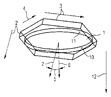
Fig. 1 shows a hexagonal crystal structure 1
with a crystal axis. A seed crystal comprising SiC is
denoted by 1. The lattice cell of the seed crystal 1 is
symbolically indicated in fig. 1. The basic area of the
lattice cell is enclosed by two vectors 3 and 4<1120>
and <1110>, respectively. A third vector 2 in the
hexagonal lattice cell, which encloses the volume of
the lattice cell, is the vector [0001]. It is identical
CA 02368380 2001-08-17
GR 99 P 3078 P - 6a -
to the crystal axis of the seed crystal 1 and, in the
illustration shown, includes
CA 02368380 2001-08-17
GR 99 P 3078 P - 7-
an angle 5 with a normal 6 to the seed crystal 1. The
normal 6 to the seed crystal 1 is perpendicular to the
surface of the seed crystal on which the SiC is
deposited from the gas phase for the purpose of forming
the bulk single crystal. In a first embodiment of the
method according to the invention, this angle 5 is
between 2 and 10 . (In this case, the angle 5 is the
angle between the direction of growth and the [0001]
vector 2 of the bulk single crystal.)
The arrow 12 indicates the direction of growth
of the crystal which is grown on, this direction being
explained in more detail below.
Figs. 2A and 2B show simplified illustrations
of the arrangement of the atoms in the lattice in the
direction of the third vector [0001] of the lattice
cell. The atoms in the SiC lattice are situated in
superposed planes. Furthermore, they adopt a defined
distance from one another in the lateral direction. In
figs. 2A and 2B, this is in each case indicated by a
grid of auxiliary lines 7. Small solid circles indicate
the C atoms 9, while larger shaded circles indicate the
Si atoms 8 in the SiC lattice.
The sequence of the atoms of an SiC crystal of
6H structure is shown in fig. 2A. It can be seen from
fig. 2A that the SiC atoms successively arrange
themselves one level higher and one level further to
the right during growth. At the fourth level, the
direction of the lateral offset is reversed, so that
the next atoms are no longer incorporated offset to the
right of the previous atom, but rather are offset to
the left of the previous atom. After another four
levels, this lateral offset is reversed again. The
number of atoms incorporated in the lattice with an
offset to the right is identical to the number of atoms
incorporated in the lattice with an offset to the left,
resulting in a "zigzag chain" with links of identical
length. The adjacent levels in figs. 2A and 2B on the
horizontal axis are denoted by A, B, C. After six
layers, a point
CA 02368380 2001-08-17
GR 99 P 3078 P - 7a -
which is equivalent to the starting point is reached. A
lattice
CA 02368380 2001-08-17
GR 99 P 3078 P - 8-
period, i.e. the distance of six layers to the first
repetition, has a length of 1.512 nm (15.12 A).
Fig. 2B shows the same situation for a 15R
lattice. The difference between the crystallization in
6H and in 15R consists in the fact that the number of
levels which are incorporated in the lattice with an
offset to the right in a 15R crystal is greater by one
than the number of levels which are incorporated in the
lattice with an offset to the left. The "zigzag chain"
no longer has links of equal length. Therefore, as it
builds up, the chain "migrates" to the right. After
sixteen layers, however, a point which is equivalent to
the starting point is reached even with the 15R
lattice. The lattice period with the 15R
crystallization is 3.73 nm (37.30 A).
To stabilize 15R SiC, it is particularly
expedient for the growth to take place in the direction
of the Si side of the polar [0001] axis. Therefore, the
seed crystal 1 is oriented in such a manner that the Si
atoms 8 form the termination on a first side 10 of the
seed crystal 1, and the C atoms 9 form the termination
on a second side 11 of the seed crystal 1. The growth
therefore takes place on the first side 10, which is
situated at the bottom in fig. 2A and fig. 2B: the
growth takes place with the growth direction 12 from
the top downward.
Figs. 3A and 3B show a device for carrying out
the method according to the invention and its
temperature profile, respectively. A crucible 13 is
arranged in a furnace 14 which, by means of heating
windings or induction coils 15, is heated to a mean
temperature of more than 2 200 C. The growth crucible
may in particular be an inductively heated growth
crucible. The SiC seed crystal 1 is attached to the
upper end (the cover) of the crucible 13. SiC powder 16
at the lower end of the crucible 13 is sublimed by the
high temperature and is deposited, as a growing SiC
bulk single crystal 17, on the seed
CA 02368380 2001-08-17
GR 99 P 3078 P - 9-
crystal 1. The temperature distribution is such that a
higher temperature prevails at the lower end of the
furnace while a lower temperature prevails at the upper
end of the furnace. This temperature profile is
illustrated in fig. 3B, in which the temperature is
plotted on the horizontal axis and the height in the
furnace 14 is plotted on the vertical axis. The
temperature field is practically rotationally
symmetrical. The temperature profile shown in fig. 3B
has a curvature and therefore a section where
d2T/dx2 = 0. This makes a significant contribution to
the uniaxial tensile stress which is required for the
15R growth.
In the latter embodiment of the method
according to the invention, the uniaxial tensile stress
is also achieved by orientation of the seed crystal 1
so that the normal to the surface of the seed crystal 1
includes a predetermined angle with the [0001] axis 2
of the bulk single crystal.
Instead of grinding the seed crystal 1 so that
it has an inclination corresponding to the
predetermined angle 5, the uniaxial tensile stress can
also be generated by means of a rotationally
symmetrical temperature field, the axis of symmetry of
which does not coincide with the crystal axis. In a
further embodiment, by contrast, the temperature field
is not rotationally symmetrical.
In addition or in a further embodiment of the
production process, the uniaxial tensile stress may be
generated by asymmetric growth. This can be achieved,
for example, by diverting the mass flow of the SiC gas
species through a diaphragm system in the furnace, so
that after a predetermined time the SiC bulk single
crystal 17 has grown further on one side than on the
other side. Consequently, the normal to the surface of
the growth phase boundary is at an angle with respect
to the [0001] axis 2 of the SiC bulk single crystal 17.
In the case of a curved phase boundary, this expression
is understood to mean the mean surface normal.
CA 02368380 2001-08-17
GR 99 P 3078 P - 10 -
A diaphragm system of this type with a diaphragm 18 is
shown in fig. 4. The diaphragm 18 is arranged in such a
way that the mass flow comprising the SiC gas phase
onto the growing SiC bulk single crystal 17 is greater
on one side of the SiC bulk single crystal 17 than on
the opposite side of the SiC bulk single crystal 17:
the principal aperture of the diaphragm 18 is not
arranged centrally with respect to the axis of symmetry
of the seed crystal 1. Consequently, vaporized SiC from
the holding region 16 flows more toward one side of the
growing SiC bulk single crystal 17, and is deposited to
a greater extent on that side of the SiC bulk single
crystal 17 which lies opposite the aperture of the
diaphragm 18 than on that side of the SiC bulk single
crystal 17 which lies "in the shadow" of the
diaphragm 18.
Moreover, a uniaxial tensile stress, the
resultant of which acts in the predetermined angle 5,
can be exerted on the SiC bulk single crystal 17 during
the growth by means of mechanical devices. A
corresponding device is shown in fig. 5. The seed
crystal 1 is arranged in a tube 19, in which the
thickness of the tube wall is dependent on the height
and on the direction perpendicular to the axis of the
tube 19. By way of example, in the embodiment shown in
fig. 5, the thickness of the tube wall at the level of
the seed crystal 1 on the left-hand side is very great,
while the opposite wall on the right is very thin. The
result is that the expansion (not illustrated) of the
tube 19 caused by the high temperature in the furnace
is greater on the side of the thick wall than at the
thin wall on the opposite side. In this way, the SiC
bulk single crystal 17 is forced into "skewed" growth.
In this context, it should be ensured that the
expansion coefficient of the material from which the
tube 19 is produced differs from that of SiC and also
from that of the surrounding crucible 13. As a result,
the temperature gradient which prevails during the
growth applies said tensile stress to the SiC bulk
CA 02368380 2001-08-17
GR 99 P 3078 P - 10a -
single crystal 17, and during cooling the SiC bulk
single crystal 17 is subject to a shear force,
CA 02368380 2001-08-17
GR 99 P 3078 P - 11 -
so that the desired asymmetric "zigzag chain" of the
atoms in the SiC bulk single crystal 17 is produced.
As well as or in addition to the axial
temperature profile which is shown in fig. 3B and is
characterized in particular by a non-vanishing second
position derivative in the axial direction, it is also
possible for an inhomogeneous radial temperature
profile within the crucible 13, in combination with an
SiC seed crystal 1 whose normal is tilted toward the
[00013] crystal direction to effect a uniaxial tensile
stress which is beneficial to the 15R growth. An
advantageous radial temperature profile of this type
can be described most easily through its isotherms. By
way of example, fig. 6 shows five non-planar isotherms
Il to 15, all of which have a curvature with a radius
of curvature R. To form a uniaxial stress which is
sufficient for rhombohedral crystal growth, it is
expedient to establish a temperature profile with
isotherms I1 to 15 whose radius of curvature is at most
4 times as great as the diameter of the growing SiC
bulk single crystal 17. In the example shown in fig. 6,
the SiC bulk single crystal 17 has a diameter of about
2 inches and the radius of curvature is 180 mm long.
With a transfer of material from the stock of SiC
powder 16 to the growing SiC bulk single crystal 17
which is homogeneous over the cross section of the
crucible 13, the non-planar, convex profile of the
isotherms Il to 15 is reproduced in a crystal growth
surface 20. This is then of the same shape as the
isotherms Il to 15.
The method according to the invention allows
the production of a-SiC bulk single crystals, in
particular with a rhombohedral 15R crystal structure,
for semiconductor wafers and substrates. SiC wafers
with a 15R crystal structure have particularly
advantageous properties for some electronic
applications, in particular MOS transistors. In further
processing steps, cubic SiC epitaxial layers for
electronic applications can be grown on the 15R SiC.