Note: Descriptions are shown in the official language in which they were submitted.
CA 02368585 2001-09-26
WO 00/60735 _ 1 _ PCT/US00/08425
NON-LINEAR DISTORTION GENERATOR
BACKGROUND OF THE INVENTION
Field of the Invention
The present invention relates generally to communication systems employing
amplification devices. More particularly, the invention pertains to a non-
linear
predistortion or postdistortion generator for coupling in-line with an
amplifier,
optical detector or laser to minimize the signal third order distortion caused
by signal
processing.
Description of the Related Art
Amplifiers are widely used in many types of communication applications.
Although it is preferable to keep amplifiers within their linear range of
operation, it
has been increasingly necessary to extend the operation of amplifiers into
high power
and high frequency regions of operation. Typically, the output power of an
amplifier
is limited by the non-linearity of the active devices, including bipolar
transistors and
I S FETs. These non-linearities result in distortions which are impressed upon
the signal
being amplified. Reducing the non-linear distortions of an amplifier results
in
increases of the output power, the system dynamic range and the carrier-to-
noise
ratio. Accordingly, minimizing distortions and achieving linear frequency
response
is paramount to efficient amplifier operation.
Additionally, laser or optical detectors used within a circuit can also
introduce
distortions. It is preferable to minimize or eliminate all of these types of
distortions.
CA 02368585 2001-09-26
WO 00/60735 PCT/US00/08425
-2-
Minimizing distortion is particularly important when a series of amplifiers is
cascaded over a signal transmission path, such as a series of RF amplifiers in
a
CATV transmission system. Disposed throughout a CATV transmission system are
RF amplifiers that periodically amplify the transmitted signals to counteract
cable
attenuation and attenuation caused by passive CATV components, such as, signal
splitters and equalizers. The RF amplifiers are also employed to maintain the
desired
carrier-to-noise ratio. Due to the number of RF amplifiers employed in a given
CATV transmission system, each RF amplifier must provide minimum degradation
to the transmitted signal.
Many amplifiers are subject to a wide range of ambient operating
temperatures. These temperature changes may affect the operating
characteristics of
certain electronic components within the amplifier, thereby inducing
additional
distortions. A temperature range of -40°C to +85°C is not
uncommon for many
amplifier applications in a communication environment. To ensure consistent
performance over the operating bandwidth, and to minimize resulting
distortions, an
amplifier must be designed for a broad range of ambient operating
temperatures.
The distortions created by an amplifier which are of primary concern are
second (even) and third (odd) order harmonic intermodulation and distortions.
Prior
art amplifier designs have attempted to ameliorate the effects of even order
distortions by employing push-pull amplifier topologies, since the maximum
second
order cancellation occurs when equal amplitude and 180 ° phase
relationship is
CA 02368585 2001-09-26
WO 00/60735 PCT/US00/08425
-3-
maintained over the entire bandwidth. This is achieved through equal gain in
both
push-pull halves by matching the operating characteristics of the active
devices.
However, odd-order distortion is difficult to remedy. Odd-order distortion
characteristics of an amplifier are manifest as cross modulation (X-mod) and
composite triple beat (CTB) distortions on the signal being amplified. X-mod
occurs
when the modulated contents of one channel being transmitted interferes with
and
becomes part of an adjacent or non-adjacent channel. CTB results from the
combination of three frequencies of carriers occurring in the proximity of
each
carrier since the carriers are typically equally spaced across the frequency
bandwidth.
Of the two noted distortions, CTB becomes more problematic when increasing the
number of channels on a given CATV system. While X-mod distortion also
increases in proportion to the number of channels, the possibility of CTB is
more
dramatic due to the increased number of available combinations from among the
total number of transmitted channels. As the number of channels transmitted by
a
communication systemincreases, or the channels reside close together, the odd-
order
distortion becomes a limiting factor of amplifier performance.
There are three basic ways of correcting distortion created by a non-linear
device (NLD): 1) reduce the signal power level; 2) use a feed forward
technique;
and 3) use a predistortion or postdistortion technique. The first method
reduces the
signal power level such that the NLD is operating in its linear region.
However, in
the case of an RF amplifier this results in very high power consumption for
low RF
output power.
CA 02368585 2001-09-26
WO 00/60735 PCT/US00/08425
-4-
The second method is the feed forward technique. Using this technique, the
input signal of the main amplification circuit is sampled and compared to the
output
signal to determine the difference between the signals. From this difference,
the
distortion component is extracted. This distortion component is then amplified
by an
auxiliary amplification circuit and combined with the output of the main
amplification
circuit such that the two distortion components cancel each other. Although
this
improves the distortion characteristics of the amplifier, the power consumed
by the
auxiliary amplification circuit is comparable to that consumed by the main
amplification
circuit. This circuitry is also complex and very temperature sensitive.
The third method is the predistortion or postdistortion technique. Depending
upon whether the compensating distortion signal is generated before the non-
linear
device or after, the respective term predistortion or postdistortion is used.
In this
technique, a distortion signal equal in amplitude but opposite in phase to the
distortion
component generated by the amplifier circuit is estimated and generated. This
is used
to cancel the distortion at the input (for predistortion) or output (for
postdistortion) of
the amplifier, thereby improving the operating characteristics of the
amplifier.
One such distortion design, as disclosed in U.S. Patent No. 5,703,530 and
shown
in Figure 1, relies upon a traditional ~-attenuation network and a delay line
for gain
compensation; and a diode pair coupled with a delay line for distortion and
phase
compensation. This circuit generates a distortion that is equal in amplitude
but opposite
CA 02368585 2001-09-26
WO 00/60735 PCT/US00/08425
_5_
in phase to the distortion introduced by the amplifier. Plots of the
distortions
contributed by the distortion generator and the distortions manifest by the
amplifier are
shown in Figures 2 and 3. As shown, the distortion signal compensates for the
distortions generated by the amplifier. However, the use of delay lines in
such a manner
is impractical since delay lines are physically large, are difficult to adjust
and the results
are inconsistent across a wide frequency range. Additionally, both amplitude
and phase
information are required for correct compensation. The '530 patent also states
that the
system disclosed therein is not ideal for certain application, such as
predistortion for
CATV RF amplifiers, due to the excessive losses introduced by the distortion
circuit.
An inline predistortion design, as disclosed in U.S. Patent No. 5,798,854,
provides compensation for NLDs by applying a predistorted signal equal in
magnitude
but opposite in phase to the distortion produced by the NLD. However, the
circuitry
disclosed therein is not matched to the NLD. Additionally, the '854 patent
presents a
design that is typical of the prior art in the use of a high resistance bias
for the diodes.
This will reduce the correction efficiency and increase the effects of
temperature upon
the circuit.
Accordingly, there exists a need for a simple distortion generator which
counteracts the distortion created by an NLD. The circuit should not introduce
additional signal delay and should operate over a wide frequency bandwidth and
wide
ambient temperature range.
CA 02368585 2001-09-26
WO 00/60735 PCT/US00/08425
-6-
SUMMARY OF THE INVENTION
The present invention is an in-line predistortion or postdistortion generator
for
coupling in-line with an NLD to produce an output signal of useful amplitude,
but with
low composite triple beat and cross modulation distortions. The distortion
generator
comprises an instant controlled non-linear attenuator which utilizes the non-
linear
current flowing through a pair of diodes to provide the proper amount of
signal
attenuation over the entire frequency bandwidth. The distortion generator
circuitry is
always matched to the NLD, thereby ensuring a frequency response that is
predictable
and predefined. The distortion generator also includes a temperature
compensation
circuit to ensure consistent operation throughout a wide temperature range.
Accordingly, it is an object of the present invention to provide a temperature
compensated distortion generator which minimizes cross modulation and
composite
triple beat distortions manifested by an NLD such as an RF amplifier, a laser
diode or
a photodetector.
Other objects and advantages of the of the present invention will become
apparent to those skilled in the art after reading a detailed description of
the preferred
embodiment.
BRIEF DESCRIPTION OF THE DRAWINGS
Figure 1 is a schematic diagram of a prior art distortion generator.
CA 02368585 2001-09-26
WO 00/60735 PCT/US00/08425
Figure 2 is a combination plot of the effect of using the outputs from the
prior
art distortion generator shown in Figure 1 with an RF amplifier.
Figure 3 is a combination plot of the effect of using the outputs from the
prior
art distortion generator shown in Figure 1 with an RF amplifier.
Figure 4 is schematic diagram of a rc attenuator.
Figure 5 is a signal diagram of the diode non-linear current caused by the
input
voltage.
Figure 6 is a schematic diagram of the preferred embodiment of the distortion
generator of the present invention.
Figure 7 is a schematic diagram of the temperature compensation circuit.
DESCRIPTION OF THE PREFERRED EMBODIMENTS
The preferred embodiment of the present invention will be described with
reference to the drawing figures where like numerals represent like elements
throughout.
Although the preferred embodiment of the present invention will be described,
for
simplicity of explanation, as being coupled with an RF amplifier, those
skilled in the art
would clearly recognize that such a distortion generator could also be
utilized to
compensate for distortion in laser transmitters, optical detectors, and other
electronic
components which operate over a wide range of frequencies. The description
herein is
not intended to be limiting, rather it is intended to be illustrative.
CA 02368585 2001-09-26
WO 00/60735 PCT/US00/08425
_8_
The present invention will be described with reference to Figure 4, whereby a
~t attenuator network 20 is shown. The network 20 comprises a selected
configuration
of resistors Zl, Rl, R2, R3, Zo, Rp. The signal source is input at signal
input 30 and the
output of the attenuator network 20 is seen across the output 95. Zl is the
source of
internal impedance which should be equal to the system impedance Zo, which is
seen
across the output 95. In an embodiment of the invention for use with a CATV
system,
the impedance values Zl and Zo are equal to 75 Ohms. Three of the resistors
Rl, R2, R3
form a ~ attenuator configuration. Preferably, the values (Y) of resistors RZ
and R~ are
equal, and substantially larger than the value (X) of resistor Rl. Resistor Rp
is
connected in parallel with resistor Rl.
As one skilled in the art would clearly recognize, when the following
condition
is satisfied:
X = 2Zo2 Y~ (YZ - Zo2) Equation (1)
the attenuator network 20 is matched at input and output, from DC to very high
frequencies. For one example of the attenuator when X = 7.5 and Y = l .SK, the
power
attenuation A for this attenuator network 20 is:
Equation (2)
2(YZo / (Y + Zo) + X)Y (YZo / (Y + Zo))
(Y + X + YZo / (Y + Zo)) (X + (YZo / (Y + Zo)))
_ (__________________________________________________________________________
Zo + (YZo / (Y + Zo) + X)Y
Y+X+YZo/(Y+Zo)
CA 02368585 2001-09-26
WO 00/60735 PCT/US00/08425
-9-
Under the condition when Zo « Y, (as is the case when X = 7.5 and Y = 1.5K):
A= (2 Zo/ (2 Zo + X))z Equation (3)
A (dB) = 10 lg A Equation (4)
When X = 7.5 and Y = 1.5k, A (dB) = 0.42dB. This means the attenuator network
20
has very low insertion losses and a good frequency response. When X has a
small
variation due to the parallel of RP, shown in Figure 4, from Equation (3)
Delta X
D elta A (dB ) - - 8 .68 Equation (5)
2Zo + X
z
Delta X _ X X R R P - X - - R P Equation (6)
From Equation (6):
2
Delta A (dB) - 8.68 X Equation (7)
2Zo RP
For example, If Rp = 375 ohms then:
7.5 7.5 _
Delta A (dB) = 8.68 150 375 0.00868dB Equation (8)
Equation (8) shows that when RP (375 ohms) is in parallel with RI (7.5 ohms),
the
attenuation will be reduced by 0.00868dB. This amount of attenuation change is
needed
for non-linear compensation for an amplifier. This example also shows that
when the
CA 02368585 2001-09-26
WO 00/60735 PCT/US00/08425
-10-
value of RP » R,, (i.e., when RP is 50 times larger than R1), adding Rp
parallel with Rl
has almost no effect on the impedance match, and the voltage drop over the RP
is mainly
determined by the value of R1.
However, if a linear resistor RP is used in the attenuator network 20, there
will
be no distortion signal produced. The attenuator network 20 as shown is a
linear device.
In order for a distortion circuit to operate effectively, diodes are used to
create a non-
linear resistance. Preferably, Schottky diodes are utilized. At small current,
diode
current is exponentially proportional to the voltage across over the diode.
Thus diodes
can be used as a non-linear resistance. For non-linear applications, the
amount of
attenuation can be calculated as:
Delta A (dB) = 8-68 2Zo R g~6g ZZo 1, Equation (9)
P
Where IP is the current flow through RP, (the non-linear resistance). I, is
the
current flow through RI. Equation 9 provides the relationship of the
attenuation change
due to the current change in IP. This equation is accurate over a broad
frequency range.
The relationship between the delta attenuation and a change in current is
still valid when
the resistance is a non-linear resistor. Accordingly, Equation 9 provides a
good
estimation of how much non-linear current is required for predistortion or
postdistortion
purposes.
CA 02368585 2001-09-26
WO 00/60735 PCT/US00/08425
-11-
Referring to Figure 5, when the input sinusoidal voltage wave changes from
V, to VZ to V3, the output current changes from I, to IZ to I3 respectively.
The non-
linear current used for third order correction is:
I nonlinear _ Il - 2 I2 + I3 Equation (10)
From Equation 9, the non-linear current needed is:
X I nonlinear
Delta A nonlinear correction (dB) = g~68 2Zo I output Equation (11)
Only non-linear current will be useful for predistortion or postdistortion
purposes. Equation 11 can be rewritten in the form of
Delta A nonlinear correction (dB) - g.6g I nonlinear eff Equation (12)
I output
I nonlinear
I nonlinear eff = R 1 / (2Zo) Equation (13)
Accordingly, I nonlinear eff in Equation 12 is the effective non-linear
current
going to the output port 114 which is shown in Figure 6. I output in Equation
12
SUBSTITUTE SHEET (RULE 26)
CA 02368585 2001-09-26
WO 00160735 PCT/US00/08425
-12-
is the total current that goes to the output port 114. Equation 13 shows that
only a
small part of the non-linear diode current is effectively being used for
correction.
The ~ attenuator network 20 has low insertion loss and the voltage drop of
the input voltage on R, (shown in Figure 4) is proportional to the input
voltage.
This voltage may be used to drive a pair of diodes to produce non-linear
current.
The non-linear current flowing in the diodes will cause an attenuator to
provide less
attenuation at larger RF amplitudes, (i.e. when the input signal has a higher
power).
This may be used to compensate for the signal compression caused by
amplification.
Because of the relatively high value of the diode's non-linear resistance, the
match
of the attenuator network is almost unchanged. This match will not be changed
even
over temperature. Additionally, frequency response over mufti-octave frequency
bands is favorable.
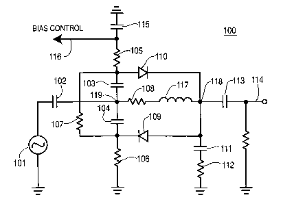
Referring to Figure 6, the preferred embodiment of the attenuator 100 for
predistortion and postdistortion is shown. The attenuator 100 of the present
invention includes several additional components that modify a traditional n
attenuator to achieve significantly better performance over a wide frequency
and
temperature range. The attenuator 100 has an input port 101, an output port
114 and
a bias control port 116. The attenuator 100 may be used in a predistortion
configuration with an amplifier or in a postdistortion configuration. For a
predistortion configuration, the output port 114 is connected to the input of
an
amplifier. For the postdistortion configuration as shown in Figure 6, an
output
signal generated by an amplifier, is applied to the input port 101. The
attenuator 100
SUBSTITUTE SHEET (RULE 26)
CA 02368585 2001-09-26
WO 00/60735 PCT/US00/08425
-13-
includes resistors 105, 106, 107, 108, 112; capacitors 102, 103, 104, 111,
113, 115;
diodes 109, 110, and an inductor 117.
In most prior art applications, an inductor is used as a phase control element
to change the correction signal phase. However, in the present invention the
inductor 117 is used in series with the resistor 108 to make a parallel
resonance
circuit with the forward biased diode capacitor. The inductive reactance
cancels the
specific capacitive reactance of the diodes. At the resonance frequency, the
capacitance of the diodes 109,110 will be compensated by the inductor 117 so
that
the impedance between points 118 and 119 will be purely resistive and can be
calculated as follows:
R impedance between 118, 119 = L / (C * R); Equation (14)
where L is the inductance of 117 in Henrys; C is the total forward biased
capacitor
in Farads; and R is the resistance 108 in Ohms. By carefully controlling L and
C,
one may get the following:
R impedance between 118, 119 = R Equation (15)
This means the capacitive effect has been totally canceled and an ideal pure
resistive
load over a very wide frequency range has been achieved.
In prior art systems, the capacitance associated with the diodes has not been
considered. In predistortion applications, Shottkey diodes are forward biased,
which
results in a greater capacitance. When an RF signal is input across the
diodes, the
SUBSTITUTE SHEET (RULE 26)
CA 02368585 2001-09-26
WO 00/60735 PCT/US00/08425
-14-
average capacitance increases. Even at a bias of 0 volts, the impedance
introduced
by the diodes capacitance may not be ignored since the capacitance in parallel
with
the PN junction of the diodes will reduce the overall voltage drop on the
diodes, thus
reducing the non-linear current produced by the diodes and the overall
correction
effect. Compensating for the capacitance associated with the diode 109, 110,
the
inductor 117 resonates with the capacitance of the diodes 109, 110 at higher
RF
frequencies, thus extending the overall frequency response of the circuit.
The function of the resistors 105, 106, 107, 108, 112 and the capacitors 102,
103, 104, 111, 113, 115 and inductance 117 is to form a modified ~c
attenuation
network in comparison to the n attenuation network 20 shown in Figure 4. The
capacitors 102,103,104,111,113, and 115 are also used for DC blocking and AC
coupling. From an AC standpoint, the parallel combination of resistors 105 and
106
is functionally equivalent to resistor R2 of Figure 4. Preferably, the values
of
resistors 105 and 106 should be chosen such that the parallel combination is
equivalent to the value of resistance of resistor 112, (i.e.
((R,os*R,o~)~(R,os+R,o6))
R,12). Resistor 108 is functionally equivalent to resistor RI of Figure 4; and
the in-
series combination of resistor 112 and capacitor 111 is functionally
equivalent to
resistor R~ of Figure 4. The value of resistor 107 has no effect on RF signal
attenuation.
The other function for resistors 105, 106, and 107 is to supply a DC bias to
the diodes 109,110. The diodes 109,110 are first connected in series; and the
series
combination is connected to resistor 107 in parallel. Because resistor 107 has
a low
SUBSTITUTE SHEET (RULE 26)
CA 02368585 2001-09-26
WO 00/60735 PCT/US00/08425
-15-
resistance value and is in parallel with the diodes 109, 110, the voltage drop
across
the diodes 109, 110 will be primarily determined by the resistance of resistor
107.
If the DC current flow in resistor 107 is much more than the current flow in
the
diodes 109, 110, the DC voltage drop across the diodes 109, 110, will be very
stable
and will be insensitive to the presence or absence of a signal at the input
port 101.
The integrated functions of signal attenuation and diode bias supply avoid any
parasitic effects due to the introduction of additional bias circuitry. This
permits a
high frequency response and a favorable impedance match.
From a DC perspective, resistor 107, in parallel with capacitors 103 and 104,
provides a dissipative circuit to the capacitors 103,104. Therefore, resistor
107 will
discharge the accumulated electric charge of connected capacitors 103,104 in
every
AC cycle.
Diode 109 is connected to resistor 108 through capacitor 104 while diode 110
is connected to resistor 108 through capacitor 103. Diode 109 is responsible
for the
RF distortion correction during the negative portion of the AC cycle, while
the diode
110 has the same function during the positive half of the AC cycle. The non-
linear
current of diode 109 charges capacitor 104, and the non-linear current of
diode 110
charges capacitor 103. Due to the configuration of the circuit, the voltage
produced
on capacitors 103 and 104 have the same value but different signs. The small
resistance from resistor 107 connected to the capacitors 103, 104 discharges
the
accumulated electric charge during every AC cycle. As a result, there is no
additional DC voltage drop across the capacitors 103, 104 due to the input RF
SUBSTITUTE SHEET (RULE 26)
CA 02368585 2001-09-26
WO 00/60735 PCT/US00/08425
-16-
signals. This permits the diode 109,110 to provide the largest non-linear
current for
the correction purpose.
The present invention has several unique advantages over the prior art. Due
to its symmetric structure, the attenuator 100 produces only odd order
distortion.
Consequently, the circuit does not degrade the second order performance of an
NLD.
The attenuator 100 also uses two low series resistances 107, 108. Resistor 107
significantly improves the correction efficiency. Resistor 108 provides for
distortion
correction with low insertion losses. Due to the attenuator 100 design, the
voltage
drop across resistor 108 fully loads the diodes 109, 110 even under non-linear
operation of the diodes 109,110. As a result, maximum non-linear current is
utilized
for correction purposes. The present attenuator design uses low series
resistance 108
in series with the inductor 117 to compensate for the capacitance of the
diodes 109,
110. Thus, this circuit may work over a wide frequency range. This correction
circuit design is flexible and may be adjusted to different kinds of RF
hybrids with
different distortion characteristics. This circuit is always matched to its
input side
and output side over wide frequency range.
Finally, proper phasing of the distortion signals is inherent in the design,
thereby avoiding additional phase circuitry and delay lines. This permits a
circuit
design which is much less complex and results in a compact and robust design.
Table 1 provides a listing of the components shown in Figure 6. However,
one skilled in the art would clearly recognize that the values shown in Table
1 are
only for explanatory purposes, and should not be considered to be limiting to
the
SUBSTITUTE SHEET (RULE 26)
CA 02368585 2001-09-26
WO 00/60735 PCT/US00/08425
-17-
invention. For example, the value of resistor 108 may range from approximately
2S2
to 30SZ. Likewise, the value of resistor 107 may range from approximately
100SZ to
3000SZ.
TABLE 1
COMPONENT VALUE OR
IDENTIFICATION
102 0.1~ f
103 0.1 ~ f
104 0.1~ f
105 6KSZ
106 6KS2
107 33052
108 7.SS2
109 HP HSMS-2822#L30
110 HP HSMS-2822#L30
111 0.1~ f
112 3KS2
113 0.1~ f
114 7552
115 O.lp f
117 l.SnH
As previously described, the attenuator 100 uses the non-linear current
produced by the diodes 109, 110 to compensate for the voltage compression
caused
by an NLD. As shown, the attenuator 100 comprises capacitance, resistance and
two
diodes. The diodes are the only components that are sensitive to temperature
change
SUBSTITUTE SHEET (RULE 26)
CA 02368585 2001-09-26
WO 00/60735 PCT/US00/08425
-18-
and the only components that require correction during operation over a wide
temperature range. There are three factors which must be taken into
consideration
when operating the attenuator 100 over a wide temperature range:
1 ) The diode operating current will change if the bias voltage remains
constant while the ambient temperature changes. Under the same input voltage
swing at the input port 101 and the same bias voltage, more non-linear diode
current
will be created as the ambient temperature rises.
2) When the ambient temperature rises, the diode will produce less non-
linear correction current for the same input signal voltage and the same diode
bias
current.
3) NLDs typically exhibit more distortion as the ambient temperature
rises. Accordingly, a higher diode non-linear current is required for
correction of the
greater distortion.
All of the temperature effects experienced by the attenuator 100 are related
to the bias voltage. Some of the effects are additive while others are
subtractive.
However, the result is that for a given temperature, there will be an optimum
bias
voltage to produce the proper correction output. Proper temperature correction
will
be achieved when there is a predefined change of bias voltage verses
temperature.
Referring to Figure 7, the preferred embodiment of the temperature
compensation circuit 200 is shown. The temperature compensation circuit 200
controls the bias of the diodes 109, 110 (shown in Figure 6) for optimum
compensation of the distortion. As shown, the temperature compensation circuit
200
SUBSTITUTE SHEET (RULE 26)
CA 02368585 2001-09-26
WO 00/60735 PCT/US00/08425
-19-
comprises two transistors 206, 213; a capacitor 216; nine resistors 201, 202,
203,
204, 207, 209, 210, 214, 215; two diodes 205, 208; and a negative temperature
coefficient thermistor 211.
The negative temperature coefficient thermistor 211 is coupled in parallel
with resistor 210 to form a temperature linearized resistance, which is
correlated to
a change in temperature. The PNP transistor 206 provides a constant current
source
through its collector to the linearized resistor combination 210, 211. The
constant
current provided by the PNP transistor 206 induces a linearized voltage change
across the resistor combination 210, 211 as the temperature changes. By
adjusting
the value of the variable resistor 202, the amount of constant current through
the
PNP transistor 206 can be changed. Therefore, the voltage swing over
temperature
can be changed. The constant current also passes through the variable resistor
209,
thereby creating a constant voltage drop that is used as a starting bias point
for bias
voltage adjustment. By selectively adjusting the resistance of resistors 202
and 209,
any combination of voltage swing and starting bias voltage can be obtained. A
NPN
transistor 213, which is an emitter follower transistor, provides the control
bias
voltage from line 217 through line 116 to the attenuator 100, as shown in
Figure 7.
The two diodes 205 and 208 are used to compensate for the junction voltage of
the
two transistors 206, 213 which change over temperature.
Table 2 provides a listing of the components shown in Figure 7. However,
one skilled in the art would clearly recognize that the values shown in Table
2 are
only for example, and should not be considered to be limiting to the
invention.
SUBSTITUTE SHEET (RULE 26)
CA 02368585 2001-09-26
WO 00/60735 PCT/US00/08425
-20-
TABLE 2
COMPONENT VALUE OR
IDENTIFICATION
201 16KS2
202 3 .3 KSZ
203 4.7KS2
204 SOKS2
205 1N4148
206
2N3906
207 2KSZ
208 1 N4148
209 1.5 KSZ
210 2KSZ
211 DKE 402N 10
212 100 S2
213 2N3904
214 100 S2
215 3KS2
216 50~ f
It should be recognized that the present invention provides an instant voltage
controlled non-linear attenuator design combined with a bias supply for
optimum
non-linear correction efficiency and bias temperature stability. Even if the
temperature compensation circuit 200 as disclosed herein is not utilized, the
preferred embodiment of the present invention provides adequate distortion
correction over a broad temperature range. When the temperature compensation
circuit 200 is utilized, the distortion compensation results can be further
improved.
SUBSTITUTE SHEET (RULE 26)
CA 02368585 2001-09-26
WO 00/60735 PCT/US00/08425
-21-
Accordingly, a trade off between the performance of the compensating circuit
and
the complexity of the circuit must be weighted.
*
SUBSTITUTE SHEET (RULE 26)