Note: Descriptions are shown in the official language in which they were submitted.
CA 02368668 2002-O1-21
Y, r
y
Beam deflector, switching system comprising beam
deflectors as well as method for selectively coupling
terminals for optical sicfinals
The invention relates to a beam deflector for deflecting a
beam of light into a selectable direction, and to a switching
system comprising a plurality of terminals for optical
signals in order for optical signals entering the switching
system through one or more terminals to be output at
selectable other terminals. In particular., the invention also
relates to a switching system for data communication systems
with fiber-optical switching systems. Furthermore, the
invention relates to a method for operating such a switching
system, in particular for a fiber-optical switching system.
From B.H. Lee and R.J. Capik "Demonstrs.tion of a very low-
loss 576x576 servo-controlled, beam-steering optical switch
fabric", a beam-steering switch is known which enables a
plurality of fiber-optical inputs to be selectively coupled
with a plurality of fiber-optical outputs . To this end, each
optical input comprises a collimator which is adjustable by
servo-control such that a light beam exiting at one terminal
end of the input impinges upon a terminal. end of the selected
optical exit and enters the same. The servo-controlled
adjustment of the plurality of collimators is mechanically
complex and a desired reduction of switching time is
difficult.
US patent no. 5,963,682 discloses a switching system for
selectively optically coupling optical inputs with optical
outputs, wherein beam directions are not adjustable by servo-
control, but by means of liquid crystal cells and the
CA 02368668 2002-O1-21
6 T is., a
2
application of specific voltage and field patterns to the
same. The electro-optical effect of the liquid crystals used
for this purpose is sufficient to attain, by the application
of electric field patterns, adequate deflection angles for
selectively driving several outputs. However, in this prior
art system, the inertance of the liquid crystal limits an
attainable switching speed and, moreover, Tosses of optical
intensity which occur when the optical signals pass through
the switching system are felt to be too high.
US patent no. 5,319,492 discloses an optical switch, wherein
an optical polymer which is non-linear in the second order is
enclosed in a cavity, to which polymer a spatially changing
electric field can be applied by means of structured
electrodes in order to produce a switchable reflection
grating, because the refractive index of the polymer can be
spatially varied by the application of the electric field. As
the cavity is mirrored, the achievable deflection angle is
increased, because an incident light beam circulates several
times in the cavity. However, when the light beam circulates
several times in the resonator, the intrinsic absorption of
the polymer material results into significant intensity
losses, so that an increase of the deflection angle is
limited by the absorption of the medium in the cavity.
It is one object of the present invention to provide a beam
deflector for deflecting an incident light beam which is
improved in particular in respect of attainable deflection
angles or/and switching times.
Moreover; it is an object of the invention to provide a beam
deflector which is better suited for use in optical data
communication systems.
In addition, it is an object of the present invention to
provide a switching system comprising a plurality of
CA 02368668 2002-O1-21
t r. !!~a- a
3
terminals for optical signals which is in particular suitable
to be employed in optical data communications systems with
high transmission rates and short switch-over times.
Furthermore, it is an object of the invention to provide a
sviitching system comprising several terminals for optical
signals which enables comparatively little losses of optical
intensity to be achieved.
According to a first aspect, the invention proceeds from a
beam deflector which comprises a plate of electro-optical
material disposed between plano-parallel mirrors, the
reflective index of said electro-optical material being
spatially changeable by the application of an electric field
pattern in the direction of extension of the plate. The
reflectivity of the mirror of the pair of mirrors facing
towards the incident light beam is less than that of the
other mirror of the pair of mirrors. As a result, the
intensity of the incident light beam reflected by the beam
deflector is higher than the intensity of the incident light
beam transmitted by the beam deflector.
In this respect, the invention is distinguished in that the
first or/and the second mirror comprises a plurality of
layers of dielectric material, the refractive indices of
which are different from each other from layer to layer.
The invention is based on the concept that the electro-
optical material is disposed in a high-quality resonator, so
that the number of circulations which parts of the incident
light beam perform in the resonator before they exit is
particularly high. This high quality of the resonator is
achieved by the use of mirrors having a high reflectivity and
a low residual transmisssivity, respectively. This is
achieved by the use of multi-layer mirrors of dielectric
materials having different refractive powers. The high
CA 02368668 2002-O1-21
t_ c 10.A x
4
quality the resonator and, as a result,
of the high number of
circulations of the beam to be deflected intensifies the
effect the electro-optical material, so that, on the one
of
hand, the deflection angles achievable with this material
is
increased as compared to a material which is passed through
only once or only a couple of times. On the other hand, it
is
possible, at a given deflection angle, to reduce the
thickness of the electro-optical material as compared to
a
system a result, it is
with lower
resonator
quality.
As
possible o reduce the electric fields to
t be applied and the
switching times, in particular when the electro-optical
material s a liquid crystal.
i
Moreover, it is possible to employ in a high-quality
resonator also electro-optical materials which have a
relatively low electro-optical effect as compared to the
known liquid crystals, but can be switched much quicker.
Preferably, the beam deflector is provided for deflecting
light having optical wavelengths, preferably light in a
wavelength range of from 0.5 ~m to 3.0 ~,m, more preferred, in
a wavelength range of from 1.0 ~.m to 2.0 ~.m and, particularly
preferred, in a wavelength range of from 1.3 ~.m to 1.7 Vim.
Preferably, electro-optical solid materials are used,
preferably lithium niobate (LiNb03) or/and gallium arsenide
( GaAs ) .
In order to increase the reflectivity of the mirrors, and
thus the quality of the resonator, preferably, several layers
of the dielectric materials have a thickness which
corresponds substantially to a value d which satisfies the
equation d = 7~/4, wherein ~, is the wavelength of the light of
the incident beam in the dielectric material of the layer. As
a result, the partial beams of the incident light beam
reflected at a front boundary surface and a rear boundary
CA 02368668 2002-O1-21
c ... ,
surface of a layer of such a thickness d interfere with each
other in constructive manner, whereas partial beams
transmitted through the layers interfere with each other'in
destructive manner.
Further, in order to increase the resonator quality, the
plate of electro-optical material has a thickness which
corresponds substantially to a value D which satisfies one of
the two formulae D = k/2 * ~, and D = (2k-1) /4 * ~,, wherein ~,
is the wavelength of the incident beam in the electro-optical
material and k is a natural number of more than O. The first
or second one of the equations is selected depending on
whether the layers adjacent to the electro-optical material
have a higher or lower refractive index than the electro-
optical material itself and whether the structure of the
mirror layer'stack adjacent to the plate of electro-optical
material is symmetrical or unsymmetrical in respect of the
plate.
A simple configuration of the mirror is obtained if the
mirror layers are made of merely two different dielectric
materials which are alternately laminated onto one another.
The refractive indices of the two mirror materials should
differ from each other as much as possible. Preferably,
silicon dioxide {Si02) and titanium oxide (Ti0) are employed
as such mirror materials. Preferred materials are also
gallium arsenide (GaAs) and aluminium arsenide (AlAs) or
aluminium gallium arsenide (AlGaAs).
In order for the intensity of the deflected light beam to be
as high as possible; the mirror of the resonator facing away
from the incident light beam is substantially fully
reflective. The mirror facing towards the incident beam could
be provided likewise substantially fully reflective to
further increase the resonator quality. However, this mirror
has a residual transmissivity which is more than five times,
CA 02368668 2002-O1-21
ae r
in particular, more than ten times the residual
transmissivity of the mirror facing away from the incident
light beam.
Preferably, the beam deflector comprises a second plate of
electro-optical material which, viewed in the direction of
the incident beam, is disposed behind the second mirror and
arranged in a further resonator formed by the second mirror
and a third mirror which is disposed plano-parallel thereto.
Preferably, said second resonator is of a higher quality than
the first resonator disposed above the former, viewed from
the incident beam. Preferably, this is achieved in that the
third mirror has a still higher reflectivity than the second
mirror. Preferably, here, too, the residual transmissivity of
the third mirror is five times, in particular, ten times less
than the residual transmissivity of the second mirror. The
high quality of the second resonator is preferably achieved
by similar means as referred to above in respect of the first
resonator, the number of mirror layers between which the
second plate of electro-optical material is disposed,
however, being higher.
If, by means of the electrode arrangements which are
spatially structured in the plane of the mirrors, electric
fields are applied to the electro-optical materials, which
electric fields change in plate direction, the refractive
index of the electro-optical material changes in plate
direction, which results into a locally changing phase
position between the incident beam and the beam emerging from
the resonator. With appropriately structured electrodes and
appropriate voltages applied thereto, the beam deflector may
thus have the effect of a phase grating which changes the
direction of the beam emerging from the beam deflector in
respect of the incident light beam. By changing the voltage
pattern applied, the direction of the light beam emerging
ww CA 02368668 2002-O1-21
c
7
from the beam deflector can then be freely varied in certain
ranges.
In order to change the direction of the deflected light beam
in two spatial directions, each electrode arrangement is
comprised of a plurality of parallel; juxtaposed stripe
electrodes, the directions of extension of the stripes of the
two electrode arrangements extending transversely, and in
particular orthogonally, to each other. Here, the electro-
optical material is provided between the two electrode
arrangements.
Such a configuration is disadvantageous in respect of the
manufacture of the beam deflector in~. that a spatially
structured electrode arrangement must be manufactured and
contacted on both sides of the plate of electro-optical
material.
According to a further aspect, the invention proceeds from a
beam deflector for deflecting a beam of light into two
spatial directions, comprising a plate of electro-optical
material disposed between a pair of electrode arrangements
and a pair of piano-parallel mirrors, the invention according
to this aspect being distinguished in that merely one of the
two electrode arrangements being spatially structured in
plate direction and the other electrode .arrangement covering
substantially the entire area of the electro-optical material
effective for the incident light beam.
Here, the structured electrode arrangement comprises
preferably two sets of stripe electrodes, the stripe
electrodes of each set being juxtaposed in parallel to each
other and the directions of extension of the stripe
electrodes of different sets extending at an angle relative
to one another, in particular orthogonally, to each other.
~ CA 02368668 2002-O1-21
t. ~ t r
In order to be able to produce electric fields independently
of each other in the electro-optical material by menas of the
two sets of electrodes, each one of the two sets of
electrodes comprises active areas which, projected to the
mirror plane, are juxtaposed. Active areas of the electrode
sets are those areas where the electrodes of the electrode
sets do substantially not shield each other and thus act on
the electro-optical material.
In the configuration where the electrode sets are provided as
stripe electrodes, preferably, the stripes comprise in
longitudinal direction, alternately, wide and narrow active
areas, the stripe electrodes of different sets intersectingly
overlapping each other with their narrow areas. At least in
the areas of intersection, the intersecting electrodes are
electrically insulated from each other.
According to a further aspect, the invention proceeds from a
switching system for selectively coupling a plurality of
optical inputs with a plurality of optical. outputs, wherein a
plurality of terminals comprising terminal ends for the
optical signals to emerge from or/and to enter as light beams
is provided, and the terminal ends are disposed spaced apart
from each other at predetermined positions and, furthermore,
a plurality of~ beam deflectors is provided such that a
separate beam deflector is allocated to each terminal end and
the light beam exiting from the terminal end allocated to the
beam deflector is directed to the same, and said beam
deflector can be driven such that at least a part of the
light beam directed thereto is directed into a selectable
direction in order to enter, possibly after further
deflections, at least one selected termina)_ end.
In this respect, the invention is distinguished in that the
beam deflector operates in reflection, i.e., the light beam
directed to the beam deflector subst<antially does not
_ CA 02368668 2002-O1-21
t an
transmit the beam deflector, but rather, the major part of
the light beam directed to the beam deflector is returned or
reflected by the same.
As compared to the conventional beam deflector operating in
transmission, wherein an intensity of the transmitted
effective beam is reduced due to reflection losses which axe
on principle unavoidable, the system according to the
invention is distinguished in that substantially the entire
intensity of the incident light beam is available to the beam
deflector also as effective beam after the desired
deflection.
Advantageously, the switching system comprises at least one
mirror which is arranged such that a light beam emerging from
any predetermined terminal end can be directed by the beam
deflector allocated to said terminal end to the mirror such
that said mirror directs said beam to a further beam
deflector which is allocated to the se7_ected terminal end.
This configuration enables the light beams to impinge with
substantially optimal orientation on the terminal end which
they are to enter, As a result, feed-in losses and thus
transmission losses are considerably reduced in the switching
system.
A particularly simple configuration of the beam deflection
via the mirror is attained if effective mirror surfaces of
said mirror are positioned in spaces between adjacent
terminal ends or between the light beams emerging from and
entering the same, respectively.
In order to reduce an overall length of the switching system,
at a given maximum deflection angle of the beam deflector and
a given distance of the terminal ends to be driven by the
beam deflector, preferably, a telescope is positioned between
the terminal ends and the beam deflectors, said telescope
CA 02368668 2002-O1-21
1~
comprising at least one objective lens through which all
beams emerging from and entering terminal ends extend. The
telescope may be a Keplerian telescope, a Galilean telescope
or any other type of telescope.
Furthermore, it is advantageous to provide a separate
telescope for each beam deflector in order for a beam
diameter of the beam emerging from the exit end, optionally
after collimation, to be adjusted as optimally as possible to
an effective diameter of the beam deflector.
For the purpose of distinction, the above-described telescope
through which all beams extend is referred to hereinbelow as
common telescope, whereas the plurality of telescopes, which
are allocated individually to the beam deflectors are
referred to hereinbelow as individual telescopes.
Another essential, though not inevitable, aspect of the
invention resides in that to provide lateral dimensions of
the beam deflectors larger than this would be actually
necessary in terms of manufacturing engineering. In
particular, a distance b in the plane of the plate of
electro-optical material along which the beam deflector can
provide a phase shift of the reflected light of 2~ should not
be selected to be smaller than is indicated by the formula
b>~.* 5* 1
2 ~n*~n~
If this dimensioning rule is observed, crosstalk from one
output channel to another output channel is largely avoided.
This aspect is particularly embodied in a switching system,
wherein a distance between adjacent terminal ends is smaller
than a distance between adjacent beam deflectors. In terms of
manufacturing engineering, for example, the structure of the
CA 02368668 2002-O1-21
.~ r
11
structured electrode arrangement could be further reduced in
size, in order to adjust the distance between adjacent beam
deflectors to the distance between adjacent terminal ends.
However; in order to reduce crosstalk: between different
output channels, the distance between adjacent beam
deflectors is selected to be larger than it would be
necessary in terms of manufacturing engineering. However, the
distance between adjacent terminal ends is then not adjusted
to the distance between the adjacent beam deflectors, but the
distance between adjacent terminal ends is reduced in order
to reduce a maximally required deflection angle of the beam
deflectors and, thus, the overall length of the switching
system.
Embodiments of the invention are described in further detail
hereinbelow with reference to the accompanying drawings,
wherein
Figure 1 is a cut schematic partial view of an embodiment of
a beam deflector according to the invention,
Figure 2 is a graphical representation of a phase curve of
a beam reflected at the beam deflector dependent
upon a wavelength of an incident beam of light,
Figure 3 is a schematic representation illustrating a
voltage pattern to be applied to an electrode
structure of the beam deflector of Figure 1 for
attaining a beam deflection,
Figure 4 is a schematic plan view of the beam deflector of
Figure 1 illustrating electrode structures for
deflecting the beam in two spatial directions,
. CA 02368668 2002-O1-21
a
6 1
12
Figure 5 is a schematic representation of a circuit for
applying voltages to the electrodes of the beam
deflector of Figure 1,
Figure 6 illustrates an embodiment of a switching system
according to the invention for selectively
coupling terminals for optical signals,
Figure 7 is an illustrative detailed representation of the
switching system of Figure 6,
Figure 8 is a schematic cross-sectional representation of a
further embodiment of the beam deflector according
to the invention,
Figure 9 shows graphical representations illustrating
reflectivity curves of the beam deflector of Fig.
8 dependent upon the wavelength of the incident
beam,
Figure 10 shows graphical representations illustrating phase
curves of the beam reflected at the beam deflector
of Figure 8 dependent upon the wavelength of the
incident beam,
Figure 11 illustrates an embodiment of an electrode
structure according to the invention for a beam
deflector,
Figure 12 illustrates a further embodiment of a switching
system according to the invention,
Figure 13 illustrates a still further embodiment of a
switching system according to the invention, and
CA 02368668 2002-O1-21
r_
13
Figure 14 illustrates a variant of a beam deflector to be
employed in the switching system accarding to
Figures 12 and 13, and
Figure 15 illustrates a variant of the detailed
representation shown in Figure 7.
A first embodiment of a beam deflector 1 according to the
invention is described with reference to Figures 1 to 4.
The structure of the beam deflector 1 is that of an optical
resonator or etalon, wherein a plate 3 of electro-optical
material is arranged between two plano-parallel mirrors 5 and
As referred to herein, an electro-optical material is any
material which has a distinct, i.e., technically utilizable,
electro-optical effect, i.e., a refractive index n of the
electro-optical material is variable by applying an electric
field to said material. To this end, it is in particular the
so-called linear electro-optical effects of the applied
electric field strength which is of interest here.
The electro-optical material selected for this embodiment is
lithium niobate (LiNb03) , for which a refractive index of n =
2.3 is assumed, said reflective index being variable by On -
5*10 4 by the application of a suitable electric voltage of
about 400 Volt to electrodes arranged at a distance from each
other of 100 ~.m.
Of the two mirrors 5, 7, between which the plate 3 of
electro-optical material is embedded, the upper mirror 5 of
Fig. 1 facing towards an incident light beam 9 has a lower
reflectivity than the lower mirror 7 facing away from the
light beam in respect of the plate 3.
~ , ~ CA 02368668 2002-O1-21
14
Fsach mirror 5, 7 is highly reflective and provided with low
self-absorption in that a plurality of layers 11, 13 of
dielectric material with different refractive indices are
alternately laminated onto each other. In the present
embodiment, titanium oxide (Ti0), for which a refractive
index nH = 2.20 is assumed;' is used as material for the layers
11 with a high refractive index and Silicon oxide (Si02), for
which a refractive index nL = 1.48 is assumed, is used for the
layers 13 with a low refractive index.
The number of alternately arranged layers 11, 13 of the upper
mirror 5 is smaller than the number of layers 11, 13 which
the lower mirror 7 is comprised of , so that the lower mirror
7 has a higher reflectivity than the upper mirror 5. In
particular, the residual transmissivities of the two mirrors
5, 7 differ so strongly from each other that merely a minimum
intensity proportion 15 of the incident beam 9 passes through
the etalon 1 in transmission and the major intensity of the
deflected beam 1? is reflected by the etalon 1.
In respect of the high quality of the resonator, the layers
11, 13 of dielectric material have a thickness dl and d2,
respectively, which corresponds to a fourth of the wavelength
of the incident beam 9 in the respective dielectric
material of the layer.
Equally in respect of the high quality of the resonator, a
thickness D of the plate 3 of electro-optical material is
adjusted to the wavelength 7~ of the incident beam 9 in the
electro-optical material. Preferably, the thickness D
satisfies one of the formulae D = k/2 * ~, and D = (2k-1)/4
wherein ~, is the wavelength of the incident beam in the
electro-optical material and k is a natural number of more
than 0. In this respect, one of the two formulae is selected
such that partial beams which repeatedly circulate in the
~ CA 02368668 2002-O1-21
r
resonator formed by~the mirrors 5 and 7 interfere with each
other in a constructive manner.
Electric fields can be applied, position-dependent, to the
electro-optical material 3 by means of two spatially
structured electrode arrangements in order to change,
position-dependent, the refractive index n of the electro-
optical material 3. An upper electrode arrangement 19 is
disposed on the upper mirror 5 and comprises a plurality of
parallel and spaced apart stripe electrodes 21. The second
electrode arrangement 23 is mounted to the lower mirror 7
below the same and likewise comprises a plurality of parallel
and spaced apart stripe electrodes 25 (:see Figure 4). The
directions of extension of the stripe electrodes 21 and 25,
in projection to the plane of the plano-parallel mirrors 5,
7, extend orthogonally to each other in order for the
deflected beam 17 to be deflected into two spatial directions
by means of the beam deflector 1, as it is described
hereinbelow.
First, be it assumed that a substantially homogeneous
electric field is applied to the entire plate 3 of electro-
optical material via the electrode arrangements l9 and 23 in
order to change the refractive index of the electro-optical
material.
Since, as described above, substantially the entire intensity
of the incident beam 9 is reflected into the exiting beam 17,
the reflectivity of the etalon 1, when being examined
dependent upon the wavelength ~,, deviates only slightly from
a 100% reflectivity R.
This is different if the phase position of the reflected beam
17 is examined in respect of the incident beam 9 dependent
upon the wavelength ~, of the incident beam 9. A graphical
representation of these phase curves is shown in Figure 2,
CA 02368668 2002-O1-21
s
' 16
wherein the points represented by the letter X indicate the
phase curve when the electro-optical material it is not
subjected to an electric field, and wherein points
represented by circles indicate the phase curve when the
refractive index of the electro-optical material 3 is
increased by the application of a correspondingly selected
field from n - 2.30 to n + ~n - 2.31. (For a better
understanding, a value of 0.01 was selected for 0n. In
practice, lower values are applied so that comparatively low
voltages are sufficient to produce the required electric
field strength.)
The depicted phase curve is obtained if four double-layers of
silicon oxide and titanium oxide are employed fox the upper
mirror 5, each having a thickness d1 = d2 - ~,j4, if the lower
mirror 7 is comprised of 16 double-layers of silicon oxide
and titanium oxide, each having a thickness of dl - d2 - 7~j4
and if the plate of electra-optical material has a thickness
D = 14.5,.
The beam deflector is provided in respect. of a predetermined
wavelength (design quality) ~,o - 1.55 ~,m such that, when no
electric field is applied; the phase difference between
incident beam 9 and reflected beam 17 is 0. If an electric
field is applied such that the refractive index of the
electro-optical material 3 changes by L\n - 0.01 at this
wavelength ?~o, a phase difference of about 1.4 is produced
between incident and reflected wave, as it is evident from
Figure 2. If stronger electric fields are applied, also
larger phase differences Ocp can be produced. In all, with the
described etalon 1, it is possible to freely adjust the phase
relation between the incident beam 9 and i~he exiting beam 17
at the design quality ~,o, over a full period of from -~t to +~.
In Figure 3, a wave front of the incident beam 9 having
entered the etalon 1 is indicated by a line 27 extending
CA 02368668 2002-O1-21
.v . s
17
parallel to the mirrors 5, 7, and a direction of propagation
of the wave front 27 is indicated by an arrow 29.
An electric voltage pattern is applied to the electrode
structure 23 through the stripe electrodes 23, said pattern
having, position-dependent, a sawtooth shape in an x-
direction transverse to the direction of extension of the
stripe electrodes 25. In response to the voltages applied, a
position-dependent change of the refractive index is: produced
in the electro-optical medium 3, which is thus likewise of
sawtooth shape in x-direction. Here, a difference between the
lowest voltage 0 applied to the electrodes 25 and the
highest voltage Umax applied to the electrodes is selected
such that the corresponding change of the refractive index n
of the electro-optical material causes a phase shift of the
reflected beam 17 of almost 2~c. Accordingly, the wave front
27 which was initially oriented in mirror direction adjusts
itself obliquely in the resonator, as it is indicated in
Figure 3 by lines 31, a phase jump of 2~i occurring from one
line 31 to the next one. As a result of the tilt of the wave
fronts 31, the direction of propagation of the wave in the
resonator 3 no longer extends orthogonally to the mirror
surfaces 5 and 7, but likewise obliquely thereto, as it is
indicated by arrows 33 in Figure 3. The direction of the beam
17 emerging from the beam deflector 1 is then accordingly
deflected in x-direction relative to the direction of the
incident beam 9.
As it is evident from the above description, the etalon 1
constitutes a phase grating for the incident beam 9 which,
when the applied voltages exhibit, position-dependent, the
sawtooth shape, constitutes a "blazed" phase grating which
enables light to be deflected in well-aimed manner into
predetermined spatial directions.
CA 02368668 2002-O1-21
. ~ ,
If voltages are now applied, position-dependent, to the
stripe electrodes 21 of the electrode arrangement 19 as well,
it is possible to deflect the beam also in Y-direction.
Figure 3 also indicates a distance b, along which the beam
deflector 1 provides a phase shift of 2;~. In the drive mode
reflected by Fig. 3, said length b corresponds to the width
of 6 stripe electrodes 25. The shortest length b attainable
with this beam deflector 1 corresponds to double the distance
between two stripe electrodes 25 if the electrode arrangement
23 is driven such that the voltages 0 and Umax are
alternately applied to respective adjacent stripe electrodes.
It is now conceivable, by reduction of 'the distance between
adjacent stripe electrodes 25, to also reduce the minimum
distance b and to thus provide a phase grating having a still
higher grating period and, as a result, higher maximum
deflection angles, which would be possible in the described
embodiment in terms of manufacturing engineering. However, a
guided and targeted deflection of the incident beam 9 is
attained with high quality it a minimum value b realized by
the drive mode is higher than
~* 5 * 1
2 ~n*~n~
In order to obtain a more profound understanding of the
operation of the electrode arrangements 19 and 23, reference
can be taken to US patent no. 4,639,091, the full disclosure
of which is incorporated herein by reference.
The beam deflector illustrated in Figure 1 can be
manufactured, for example, in that the plate 3 is cut from a
lithium niobate monocrystal in suitable manner and then,
first, the mirrors 5 and 7 are laminated on the respective
sides of the plate by vapor deposition and, finally, the
. CA 02368668 2002-O1-21
19
electrode arrangements 19 and 23 are attached on the mirrors
and 7, respectively.
Figure 5 is a schematic representation of an electronic
circuit suitable for applying voltage patterns to two
electrode arrangements, each including 32 stripe electrodes,
in order to deflect an incident light beam 9 in x-direction
as well as in y-direction into 32 different spatial
directions. The circuit comprises a low-voltage part 35, laid
out, for example, in CMOS technology, as well as a high-
voltage part 37. Data words, each encoding a desired
deflection direction, are serially read-in, via an input SI,
into a shift register 41 and transferred in parallel from the
same to an address register 42, a clock input CL and a load
command input LD being, in addition, provided for this
purpose. Furthermore, the circuit comprises two memories
designated MEMX and MEMY in which voltage patterns for
voltages to be applied to the stripe electrodes 25 and 21 are
stored in order for a beam deflection into the desired
spatial directions to be performed. The encoding of the words
read-in into the shift register 41 is selected such that it
can be directly used via the address register 42 to
respectively address the corresponding voltage pattern in the
memories MEMX and MEMY. The addressed voltage patterns are
then supplied from the memories MEMX and MEMY to 64 digital-
to-analog current converters which supply, allocated to each
electrode 21; 25, a current to lines 41 connected to the
high-voltage part 37 where the supplied currents are
respectively converted into a corresponding high voltage
between 0 and 400 volt by means of transistors T and
resistors R and then supplied to terminals 43 for the
respective stripe electrodes 21, 25.
Further, in Figure 5, reference sign BS designates a bias
voltage for the transistors and reference sign HV designates
a terminal for supplying the high-voltage.
CA 02368668 2002-O1-21
The beam deflector described above can be employed, for
example, in a switching system for selectively coupling a
plurality of inputs and outputs for optical signals which
are, for example, input and output via light conductors. An
example of a switching system for selectively coupling
optical fibers employing a conventional beam deflector is
disclosed in US patent no. 5,963,682, the full disclosure of
which is incorporated herein by reference.
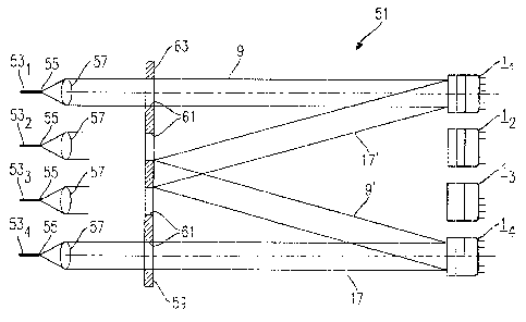
Figures 6 and 7 schematically show partial views of a
embodiment of the switching system 51 according to the
invention. A plurality of optical fibers 53-1, 53-2, 53-3,
53-4 constitute the terminals for optical signals of the
switching system 51, wherein terminal ends 55 of the fibers
53 are arranged as a two-dimensional field with equal grating
distance a in x-direction and y-direction. To this end, a
support for the fiber ends is provided, wr~ich is not shown in
the drawings, said support also holding a plurality of
collimator lenses 57 such that a lens 57 is positioned in
front of each fiber end 55 in order for the light emerging
from the fiber end 55 to be collimated as parallel beam 9
and, respectively, to feed a parallel beam 17 impinging on
the lens 57 into the corresponding fiber 5:3.
~ A separate beam deflector 1-1, 1-2, 1-3, 1-4 is allocated to
each terminal 53-1, 53-2, 53-3, 53-4 such that a field of
beam deflectors 1 is positioned spaced apart from the fiber
ends 55 such that beams 9 exiting from the fiber ends 55
impinge directly on a beam deflector l allocated to the same.
A plate 59 is disposed between the field of fiber ends 55 and
collimator lenses 57 and the field of deflectors 1
perpendicular to the beam direction and comprises holes 61
likewise spaced apart from each other by the distance a for
the beams 9, 17 to pass therethrough. A surface 63 of the
- CA 02368668 2002-O1-21
21
plate 69 facing towards the field of beam deflectors 1 is
mirrored.
Figure 6 illustrates a switch situation of the switching
system 51, wherein the upper optical terminal 53-1 of the
Figure is coupled, as input, with the lower optical terminal
53-4 of the Figure, as output. To this end, the electrode
structure of the upper beam deflector 1-1 of Figure 6 is
driven such that the beam 9 emerging from the optical input
53-1 is reflected; as beam 17', through such an angle that
the reflected beam 17' impinges on the mirrored surface 63 of
the plate 59 such that it is, in turn, reflected as beam 9'
by the same and impinges on the lower beam deflector 1-4 of
Figure 6 which is allocated to the optical output 53-4. The
lower beam deflector 1-4 is driven here such that the beam 9'
incident thereupon is reflected into the beam 17 which is fed
into the optical output 53-4. Thus, the fiber 53-1 is, as
optical input, coupled to or connected with the fiber 53-4,
as optical output.
However, it is also possible to couple the fiber 53-1, as
optical input, with the fiber 53-2, as optical output, in
that the deflector 1-1 is driven such that the beam 17'
reflected by said beam deflector is directed to the mirror
surface 63 such that the beam 9' reflected by the mirror
surface 63 impinges on the beam deflector T-2 which then, in
turn, is driven such that the beam 9' impinging thereon is
fed into the fiber 53-2, as optical output.
It is thus possible to couple a plurality of terminals 53 of
the switching system 51 in freely selectable manner in that
the beam deflectors 1 allocated to the terminals to be
coupled are appropriately driven.
In the embodiment shown in Figures 6 and 7, in operation,
every second terminal 53 is provided as input and every
~ CA 02368668 2002-O1-21
y
22
second other optical terminal 53 is provided as output, as it
is illustratively shown in Figure 7, wherein the positions of
the terminals 53 used as optical inputs are. represented as
black circles and the positions of the terminals 53 used as
optical outputs are represented as white circles.
However, it i:s also possible to use every terminal as input
or output, as required. Further, it is also possible to
provide different or modified distances between adjacent
terminal ends. An illustrating example is schematically shown
in Fig. 15.
In the following, variants of the embodiments of the
invention shown in Figures 1 to p are described. Components
which are equivalent i.n structure and function to those of
Figures 1 to 7 are designated by the same reference numerals,
for the purpose of distinction, however, supplemented by an
additional letter. For the purpose of illustration, reference
is made to the entire above description.
Figure 8 schematically shows a beam deflector la provided as
double-resonator or double-etalon structure. Similar to the
etalon shown in Figure l, the deflector la comprises a highly
reflective upper mirror 5a comprised of layers of dielectric
materials which faces towards an incident beam 9a. Below the
mirror 5a, there is provided a plate 3a made of electro-
optical material which is delimited at the bottom by a
further mirror 7a which is likewise comprised of a plurality
of layers of dielectric material.
Below the mirror 7a, there is a second plate 71 of electro-
optical material and, below the second plate 71, there is
provided a further mirror 73 likewise comprised of a
plurality of layers of dielectric material having different
refractive indices.
, CA 02368668 2002-O1-21
c
23
The number of layers of dielectric material of the lower
mirror 73 is higher than the corresponding number of the
central mirror 7a which, in turn, is higher than the number
of dielectric layers of the upper mirror 5a. Accordingly, the
upper plate 3a of electro-optical material is enclosed in a
resonator formed by the two mirrors 5a and 7a which is of
lower quality than an optical resonator formed by the mirrors
7a and 73 in which the lower plate 71 of electro-optical
material is enclosed.
The entire structure consisting of the mirrors 5a, 7a anal 73
as well as of the plates 3a and ?1 of electro-optical
material is enclosed between electrode arrangements 19a and
23a. As in the etalon structure 1a, the rear mirrors of the
two resonators are also provided to have a reflectivity which
is substantially higher than that of, the respective front
mirrors, here, too, the major part of the intensity of the
incident beam 9a is reflected as beam 17a. Figure 9
illustrates the dependency of the reflectivity of the
structure shown in Fig. 8 on the wavelength ~,. The curve
marked by crosses reflects the curve for a structure wherein
the mirror 5a is comprised of 8 layers; the mirror 7a is
comprised of 12 layers and the mirror 73 is comprised of 22
layers. The curve marked by circles reflects the curve for a
structure wherein the mirror 5a is comprised of 6 layers, the
mirror 7a is comprised of 8 layers and the mirror 73 is
comprised of 22 layers. The curve marked by the letter x
reflects the curve for a structure wherein the mirror 5a is
comprised of 4 layers, the mirror 7a is comprised of 6 layers
and the mirror 73 is comprised of 22 layers.
It was found that in all mirror embodiments the reflectivity
is extremely high.
Accordingly, with such a configuration, a phase shift of more
than 2~t can also be achieved with wavelengths which differ
CA 02368668 2002-O1-21
' v ' a
24
from the design quality ~,o, which is particularly of
importance with a view to the deflection of the beam in two
spatial directions.
Figure 10 is a representation corresponding to that of Fig: 2
of the phase difference between incident and exiting beam for
the etalon structure of Fig. 8, the mirrors 5a, 7a and 73
being comprised of 6, 8 and 22 layers, respectively, the
thickness of the plates 3a and 71 being 14.5, and 10.5,,
respectively.
The main difference between the etalon of Fig. 1 and Fig. 8
resides in that, in the beam deflector la of Fig. 8, both
resonators can each contribute to the entire phase difference
with a maximum phase difference of 2~, so that phase
differences of 4~t can very easily be attained with this
double-resonator configuration.
The structure la shown in Figure 8 can, for example, be
manufacture in that, first, the electrode arrangement 23a is
deposited on a substrate (not shown in the Figure) and, next,
the layers of the mirror 73 are vapor-deposited thereon.
After the mirror 73 has been finished., the plate 71 of
electro-optical material, such as lithium niobate, may be
grown thereon by means of MOC~TD (metal organic chemical vapor
deposition). Subsequently, the mirror 7a is vapor-deposited
and, next, the plate 3a of lithium niobate is grown by means
of MOCVD. Next, the mirror 5a is vapor-deposited and,
finally, the upper electrode arrangement 19a is applied.
By means of MOCVD a plurality of electro-optical materials
can be deposited with sufficient precision and required
material structure in order for the optical effects required
for the present invention to be attained. For further details
of the MOCVD technique, reference is made to the article of
Ren Xu "The Challenge of Precursor Compounds in the MOCVD of
y~ CA 02368668 2002-O1-21
Oxides' from http://www.tms.org/pubs/journals/JOM/9710/Xu of
January 16, 2001, the disclosure of which is also
incorporated herein by reference.
The double-resonator la, the phase curve of which is shown in
Figure 10, is configured for a design quality 7~0 of 1.55 ~,m,
the operating point at the design quality being positioned in
the area of the phase jump shown in Fig. 10.
Figure 11 illustrates a variant of the upper electrode
arrangement 19a for a beam deflector of the invention. Here,
the electrode arrangement 19a is not only comprised of stripe
electrodes which extend in parallel only in one direction.
Much rather, the electrode arrangement comprises two sets of
stripe electrodes, one set thereof extending, with stripe
electrodes 21a, in horizontal direction in Fig. 11 and a
second set of stripe electrodes extending, with strip
electrodes 25a, in vertical direction in Fig. 1l.
If, for example, an electrode arrangement 19a of the type
shown in Fig 1l is disposed, for example, on the top of the
beam deflector of Fig. 1, it suffices to correspondingly
provide the electrode arrangement 23 on the bottom of the
beam deflector as continuous and uninterrupted earth
electrode. Nevertheless, the reflected beam can be deflected
into two spatial directions. This configuration of the
electrode arrangement 19a is advantageous in that merely one
of the two electrode arrangements must be' provided in
structured manner.
In order to avoid an overlap of the electrodes provided as
intersecting stripes, the stripes 21a, 25a comprise in length
direction, alternately, wide surface areas 81 and narrow
surface areas 81, with intersecting stripes overlapping each
other merely in narrow surface areas 83. The wide surface
areas 81 are substantially surface-covering and non-
~ ~ CA 02368668 2002-O1-21
r
26
overlapping so that the electric potentials applied thereto
can act on the dielectro-optical materials. The intersecting
areas 83 of the stripes 21a and 25a, respectively, are
electrically insulated from each other. This can be achieved
in that the first partial electrode set with the stripes 25a
is applied by means of a thin-film technique, an insulating
layer is applied thereon and the other partial electrode set
with stripe electrodes 21a is disposed thereon.
However, it is also conceivable to provide the stripe
electrodes 21a of the partial electrode set disposed remote
from the electro-optical material as stripes of approximately
uniform width, because the effect of these electrodes on the
electro-optical material in the areas where these stripes 21a
overlap the stripes 25a therebelow is shielded by the stripes
25a positioned therebelow, so that effective areas of the
continuously wide outer stripe electrodes exhibit a
configuration approximately similar to that of the wide areas
81 shown in Fig. 11.
A switching system 51b shown in Fig. 12 for selectively
coupling optical inputs 53b has a structure which is similar
to that shown in Fig. 6. In contrast thereto, a common
telescope 87, which is schematically depicted in the form of
a diverging lens 89 and a collective lens 91, is positioned
between a field of beam deflectors 1b and a plate 59b
comprising a mirrored side 63b. All beams extending between
the terminals 53b and the beam deflectors 1b pass through the
collective lens 91 as well as through the diverging lens 89.
The telescope 87 substantially serves to reduce the overall
length of the switching system 51b as compared to the overall
length which must be selected for the switching system
according to Fig. 6 at a predetermined maximum deflection
angle of the beam deflectors.
~ ~ CA 02368668 2002-O1-21
27
Moreover, the switching system 51b comprises a plurality of
individual telescopes 93 such that an individual telescope 93
is positioned in front of each beam deflector 1b for
adjusting a beam 9b collimated by a lens 55b in front of the
exit end of the fiber ends 53b to the diameter which
substantially fully illuminates the effective area of the
beam deflector 1b.
It is also evident from Fig. 12 that a distance between
adjacent fiber ends 53b is smaller than a distance between
adjacent beam deflectors 1b. Although it would be possible,
in terms of manufacturing engineering, to further reduce the
distance between adjacent beam deflectors 1b, the individual
beam deflectors 1b are so configured that the above-mentioned
lower limit for the distance in the electro-optical material
along which a phase shift of 2n is produced is maintained.
The switching system 51b shown in Fig. 12 can be modified in
that both the large telescope 87 or,~and the individual
telescopes 93 can be omitted so that the.;e components are, as
such, optional.
A switching system 51c shown in Fig. 13 again serves to
selectively couple a plurality of optical inputs and outputs
53c by means of a plurality of beam deflectors lc, each of
which is allocated separately to an optical terminal 53c.
Collimator lenses 57c respectively collimate the beams
emerging from fiber ends 55c onto the beam deflectors lc.
Similar to the embodiment of Fig. 6, an incident beam 9c
reflected by a beam deflector lc is reflected into a beam
17'c which is reflected from a mirror 63c as beam 9'c onto
the beam deflector lc which is allocated to the desired exit
terminal: However, the mirror 63c reflecting the beam 17'c
back into the beam 9'c is not provided at an apertured plate,
as in Fig. 6. Rather, the mirror 63c is positioned outside of
the beam path between the collimator lenses 57c and the beam
~ ~ CA 02368668 2002-O1-21
28
deflectors lc. For this purpose, a semi-transparent feed-out
mirror 97 is provided. The beams 9c and 17c pass through said
feed-out mirror 97 between the collimator lenses 57c and the
beam deflector lc. As a result, the feed-out mirror 97 has a
polarizing effect on theses beams and only the polarized
parts of the beams 9c and 17c transmitted through the mirror
97 are then reflected, after a polarization rotation at a ~,-
quarter-plate 99, by the mirror 97 onto the mirror 63
positioned outside of the beam path.
As the feed-out of the beams to be reflected at the mirror
63c by means of the polarizing mirror 97 entails a loss of
half the intensity (due to the polarizing effect), a further,
polarizing beam divider 101 is provided between the
collimator lenses 57c and the mirror 97 in order to feed-out
the polarization part which would get lost at the mirror 97
and to direct the same to a further field of beam deflectors
1'c. These beam deflectors are driven such that they couple
the same optical inputs and outputs 53c with each other which
are also coupled with each other via the beam deflectors lc.
To this end, the beam deflectors 1'c reflect the beams
incident thereupon to a mirror 63'c which corresponds to the
mirror 63c. Equally, an inclined, semi-transparent and
likewise polarizing mirror 97' is positioned between the
mirror 63'c and the beam deflector 1'cwhich corresponds to
the mirror 97, just as a ~,-quarter-plate 99' is positioned in
front of the beam deflectors lc'.
In all, the switching system 51c' is configured such that the
optical wavelengths for both polarization direction are
substantially of equal length so that also short optical
pulses which are separated into their two polarization
directions via the mirror 101 are, after deflection at the
beam deflectors lc and 1'c, respectively, recombined at the
mirror 101 substantially correct in time.
CA 02368668 2002-O1-21
29
In the above-described embodiments, lithium niobate has been
used , as electro-optical material. However, it is also
possible to use gallium arsenide (GaAs) as electro-optical
material, for which a refractive index n = 3.5 is assumed. It
is then recommended for the dielectric layers of the
resonator mirror to be alternately comprised of aluminium
arsenide (AlAs), for which a refractive index NL - 3.0 is
assumed, and gallium arsenide (nH - 3.5). Gallium arsenide,
too, exhibits an electro-optical effect, i.e., a change of
the refractive index in response to an applied electric
field. In this respect, the intensifying effect of the
electro-optical effect can be utilized by use of so-called
"quantum well" structures in the gallium arsenide. This
technology is described in US patent no. 4,525,687, the full
disclosure of which is in this respect incorporated by
reference .
The use of semi-conductors as materials for the plate of
electro-optical material is advantageous in particular also
in so far as, in such semi-conductor materials, physical
effects, such as the !'quantum confined stark effect" and the
"Franz-Keldisch effect", can be utilized to increase the
electro-optical effect.
In the above-described embodiments, the electrode
arrangements engage around both the plates of electro-optical
material and the mirrors made of layers of dielectric
material. However, it is also conceivable to arrange the
electrode arrangements between the plate of electro-optical
material and the layered mirrors. This esnables, on the one
hand, a smaller electrode distance to be attained with a view
to an increase of the electric field strength. On the other
hand, leak currents can be avoided which might be produced in
the mirror layers. In order to reduce absorption losses at
the electrode arrangements, the latter can then be arranged
in the resonator such that they are" spaced apart from the
< < , . ~ CA 02368668 2002-O1-21
L r
resonator mirrors such that they are positioned in
oscillation knots of the light field.
In the embodiments described above with reference to' Figures
12 and 13, the structure of the beam deflectors is that
described with reference to Figures 1 to 11. However, it is
also possible to provide the optical switching systems shown
in Figures 12 and 13 with beam deflectors, each comprising a
mirror which is mechanically pivotable in respect of a mirror
support. Such beam deflectors can be manufactured in
miniaturized form and are described, for example, in the
article of James A. Walter "The future of MEMS in
telecommunications networks", Journal Michromech. Microeng.
10 (200) R1-R7/PII: 50960-1317(00)06735-8. Figure 14
schematically shows a beam deflector lc provided as so-called
MEM mirror. A circular mirror surface 103 is punched out of a
plate material 101, with pairs of hinges 105 and 106 which
are diametrically opposed in respect of the mirror surface
respectively supporting the mirror surface 103 cardanically
relative to the remaining plate material 101. Below the
mirror surface 103 , there are provided four sectors of drive
electrodes 109 on an electrode support 111 spaced apart from
the rear side of the mirror by a little distance, said
electrode support being fixedly connected to the plate
material holding the mirror surface 103. By applying
appropriately dimensioned electric voltages to the sector
electrodes 109, an electrostatic field is produced between
the mirror 103 and the electrodes, said field imparting
mechanical shift forces on the mirror surface 103 so that the
latter is pivoted about the hinge webs 105 and 106,
respectively, in order for the mirror surface 103 to be
inclined in respect of its support and to set a desired
deflection angle for incident light beams.