Note: Descriptions are shown in the official language in which they were submitted.
CA 02369015 2001-09-26
1
DESCRIPTION
LIGHT-EMITTING ELEMENT MATRIX ARRAY
TECHNICAL FIELD
This invention relates to a light-emitting element
matrix array, particularly to a light-emitting element matrix
array in which a light up state of light-emitting element may
be controlled by a small control current.
BACKGROOND ART
In an light-emitting element array used in an optical
printer, it is essentially required to derive the same number
of lines from light-emitting elements as that of light-
emitting eleattents . A wire bonding method is generally used
for the derivation of lines. Therefore, the following
problems are caused as the. density of light-emitting elements
is increased.
( 1 ) A product cost becomes larger due to the. increase of an
area of a wire bonding pad on a light-emitting element array
chip, i.e. an area of a chip.
( 2 ) A production cast becomes larger due to the increase of
the number of wire bondings.
(3) A production becomes difficult as a pitch of wire bonding
becomes smaller.
(4) A product cost is increased because driving circuits, the
number thereof is equal to that of light-emitting elements,
are generally required.
An area of one bonding pad is several times or more
compared with an area of one light-emitting element, so that
the increase of light-emitting elements density leads to the
CA 02369015 2001-09-26
2
increase of chip area.
In order to avoid these problems, a light-emitting
element including a shift register, a light-emitting diode
(LED) matrix array, and a light-emitting thyristor matrix
array have been proposed heretofore.
The LED matrix array as shown in Fig.l has resolved
above-described problems by providing a plurality of light-
emitting diodes in one line on an insulating substrate, and
constituting a matrix with an anode side and a cathode side
to decrease the number of terminals derived from the array.
In Fig.l, one or more of light-emitting diodes L" L" L"
'-' may be lighted up by a combination of levels of anode
electrodes A, - A, and levels of cathode-selecting lines K, -
K,. When an anode electrode A1 is at a High (H) level and a
cathode selecting line Kj a Low (L) level, a light-emitting
diode L~"~i-1~ is lighted up. However, a current flows from an
anode driver (not shown) to a cathode driver (not shown)
through a light-emitting diode, so that both of drivers
require a large current driving capacity, resulting in the
cost increase of driver ICs.
Inorder to resolve this problem, a light-emitting
thyristor matrix array using a light-emitting thyristor of
pnpn-structure in place of a light-emitting diode has been
proposed. Fig.2 shows the light-emitting thyristor matrix
array. According to this matrix array, a plurality of light-
emitting thyristors T" Ts, T" ~~~ are arrayed in one line.
These thyristors are divided into groups four by four.
Anodes of thyristors in each group are commonly connected to
anode terminals A" A2, A" ~~- , respectively, gates of
thyristors in each group are separately connected to gate-
CA 02369015 2001-09-26
3
selecting lines G, - G, , and cathodes of all the thyristor
are commonly connected to a cathode line K. The lighting up
of thyristors T" Tz, T" ~~~ is determined by a combination of
levels of gate-selecting lines G, - G, and levels of anode
terminals A" A~, A" ~~ . As this matrix array is a type of
cathode common, when the cathode line K is at L level and an
anode terminal A; is at H level while one gate-selecting line
Gi being at L level and the others H level, a light-emitting
thyristor Ti"it_1~ is lighted up.
The gate-selecting lines only give trigger signals, so
that the lighting up of the thyristors may be controlled by a
small current driving capacity. As a result, the cost of a
driving IC may be decreased. For this matrix array using a
light-emitting thyristor, Japanese Patent has already been
issued to the present applicant (Japanese Patent No.2807910).
However, there is . a problem such that the product cost
thereof is high because such thyristor uses a pnpn-structure.
DISCLOSURE OF THE INVENTION
The object of the present invention is to provide a
light-emitting .element matrix array in which 'a function'
equivalent to a light-emitting thyristor may be implemented
by elements different therefrom.
According to the present invention, a function of a
light-emitting thyristor may be implemented by a combination
of a transistor and light-emitting diode (LED). In this case,
an LED may be fabricated by emitter and base layers or base
and collector layers of a transistor, so that the
combinational element of a transistor and an LED may be
implemented from a three-layer structure of npn or pnp.
CA 02369015 2001-09-26
4
Therefore, the thickness of an epitaxial film becomes thinner
compared with a light-emitting thyristor of a four-layer
pnpn-structure, resulting in a low cost of products.
Furthermore, a light-emitting element matrix array in
which a light up state of light-emitting element may be
controlled by a small control current may be implemented by
integrating transistors and LEDs in the same wafer.
Accordingly, the number of terminals derived from a light
emitting element matrix array chip may be decreased, thereby
reducing an area of the chip. As a result, a high resolution
light-emitting element matrix array may be easily provided.
BRIEF DESCRIPTION OF THE DRAWINGS
Fig.l shows a conventional LED matrix array.
Fig.2 shows a conventional light-emitting thyristor
array.
Fig.3A is a plan view of a combinational element.
Fig.3H is a cross-sectional view taken along X-X' line
in Fig.3A.
Fig.4 is an equivalent circuit diagram of the
combinational element.
Fig.5 shows a fabricating process for the combinational
element.
Fig.6 shows a light-emitting element matrix array of the
first embodiment.
Fig.7 shows a light-emitting element matrix array of the
second embodiment.
Fig.8 shows a light-emitting element matrix array of the
third embodiment.
CA 02369015 2001-09-26
BEST MODE FOR CARRYING OUT THE INVENTION
A preferred embodiment of a light-emitting element
matrix array according to the present invention will now be
described with reference to the drawings.
5 Emboditnent 1
Referring to Figs.3A and 3B, there is shown a
semiconductor element consisting of a combination of a
transistor and a light-emitting diode (LED), the
semiconductor element constituting a light-emitting element
matrix array of the present embodiment. The semiconductor
element is referred to as a combinational element hereinafter.
Fig.3A is a plan view and Fig.3B a cross-sectional view taken
along X-X' line in Fig.3A. Fig.4 shows an equivalent circuit
diagram of the combinational element. The transistor may be
fabricated by depositing three layers epitaxial film of npn-
structure consisting of a first n-type semiconductor layer 21,
a p-type semiconductor layer 22, and a second n-type
semiconductor layer 23 on a semi-insulating GaAs substrate_20,
followed by mesa isolating with an etching process.
Reference numeral 10 designates an emitter terminal, 11 a
base terminal, 24-an ohmic electrode for an n-type layer (an
emitter electrode), 25 an ohmic electrode for a p-type layer
(a base electrode), 26 an ohmic electrode for an n-type layer
(a collector electrode).
On the other hand, the LED is fabricated by removing the
second semiconductor layer 23 from the npn-structure (21, 22,
23). Reference numeral 12 designates an anode terminal, 27
an ohmic electrode for an n-type layer (a cathode electrode),
2B an ohmic electrode for a p-type layer (an anode electrode).
The cathode electrode 27 of an LED and the collector
CA 02369015 2001-09-26
6
electrode 26 of a transistor is connected to each other via a
line 30.
Referring to Fig. S, there is shown a fabricating process
for the above-described combinational element. First, three
layers epitaxial film of npn-structure consisting of the
first n-type semiconductor layer 21, the p-type semiconductor
layer 22, and the second n-type semiconductor layer 23 are
deposited on the semi-insulating GaAS substrate 20. Then,
the collector electrode 26 is formed on the n-type layer 23.
Then, the n-type layer 23 is removed with a part thereof
remained, the part having the collector electrode 26 thereon.
Next, the base electrode 25 for a transistor and the anode
electrode 28 for an LED are formed on the exposed p-type
layer 22. Then, the p-type layer 22 is,etched away to form a
transistor island 32 and an LED island 34, respectively.
Next, the emitter electrode 24 and the cathode electrode 27
are formed on the exposed n-type layer 21, followed by an
annealing process. Then, the n-type layer 21 is etched away
to isolate the transistor and LED in a mesa-structure. Next,
a protective film 40 is deposited on the overall structure,
contact-holes are opened therein on each electrode 24, 25, 26,
27, 28, and lines are formed on the protective film 40.
In the present embodiment, epitaxial films as shown in
Table 1 are used. Material for all the films is GaAs.
AuGe/Ni/Au is used for electrodes for an n-type layer and
AuZn/Au is used for electrodes for a p-type layer.
CA 02369015 2001-09-26
7
Table 1
Dopant Impurity Film Note
Concentration Thickness
1 O1'/cm'
Substrate C r - Semi-
insulating
First n-layer S i 2 0 0 . 2
P-layer Z n 1 0
Second n-layerS i 1 0 0 . 1
In the present embodiment, while the first n-type layer
is used as an emitter of the transistor and the second n-type
layer as a collector of the transistor, the first n-type
layer may be used as a collector of the transistor and the
second n-type layer as an emitter of the transistor.
While the embodiment has explained as to an npn-
structure, a pnp-structure may also be used.
According to the combinational element consisted of a
transistor and LED, an LED may be lighted up by causing the
emitter terminal 10 zero volts and both the base terminal 11
and the anode terminal 12 H level.
Fig.6 shows an embodiment of a light-emitting element
matrix array structured by arraying a plurality of
combinational elements. In this embodiment, a plurality of
combinational elements each consisting of a transistor Tr and
a light-emitting diode L are divided into groups four by four.
The bases of transistors in each group are separately
connected to base-selecting lines B, - B, of bus structure,
and the emitters of all the transistors are commonly
connected to an emitter line E. The anodes of LEDs in each
group are connected to common anode terminals A" Az, A" -~~ ,
respectively. One or more light-emitting diodes may be
CA 02369015 2001-09-26
8
selected by a combination of the levels of base selecting
lines B, - B, and the levels of anode terminals Ai, A~, A" ~~ .
For example, the light-emitting diode Lj"~s_l~ may be selected
to light up when both the anode terminal Ai and the base
s selecting line Bj are at H level.
Embodiment 2
While the base side of transistors is formed as a bus
structure in the embodiment 1, the anode side of LEDs may be
formed as a bus structure. Fig.7 shows an embodiment 2 in
which the anode side of LEDs is formed as a bus structure.
The anodes of LEDs in each group are separately connected to
anode-selecting lines A1 - A, of bus structure, and bases of
transistors in each group are connected to common base
terminals B" H~, B" ~~~, respectively.
According to this light-emitting element matrix array,
the light-emitting diode L~"~j_,~ may be selected to sight up
when both the anode-selecting line Ai and the base terniinal
B~ are at H level.
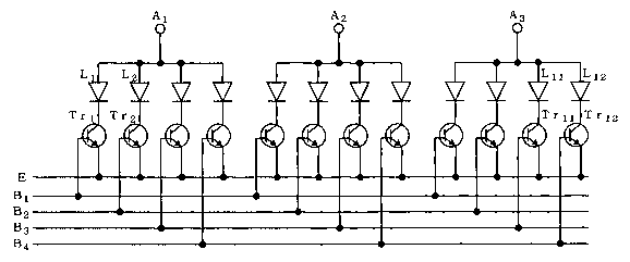
Embodiment 3
Fig.8 shows a variation of the embodiment 2, in which
one transistor Trl, Tr" Tr" w~ may be provided with respect
to a plurality of LEDs included in one group, respectively,
as shown in the figure, without providing one transistor with
respect to one LED. The base of each transistor is connected
to a base terminal B1, Bz, B, w, respectively. According to
this embodiment, a product cost may be decreased because an
area of elements is reduced by the area corresponding to the
reduced transistors.
INDUSTRIAL APPLICABILITY
CA 02369015 2001-09-26
9
According to the present invention, the function
corresponding to that of a light-emitting thyristor may be
implemented by a combinational element consisting of a
transistor and LED, and the combinational element may be
fabricated by three-layer structure of npn or pnp, therefore
it is possible to decrease the cost of the light-emitting
element matrix array.