Note: Descriptions are shown in the official language in which they were submitted.
CA 02369449 2002-01-24
Specification
Title of the Invention
Channel Data Extracting Circuit and Extracting Method
Background of the Invention
The present invention relates to a channel
data extracting circuit and extracting method for
extracting data from a byte-multiplexed frame for each
channel in SDH (Synchronous Digital Hierarchy).
Conventional SDH data multiplexing formats
include STM (Synchronous Transfer Module)-1 (bit rate:
150 Mbps), STM-4 (600 Mbps), and STM-16 (2.4 Gbps).
These multiplexing formats cannot efficiently use a
transmission channel in containing packet data such as
PPP (Point to Point Protocol).
Virtual concatenation, which is a technique
for solving this problem, can assign to an SDH channel
an arbitrary band (VC (Virtual Container)-3 (50 Mbps) x
n, VC-4 (150 Mbps) x n). For example, in STM-16, 48
VC-3 are multiplexed, and the channel band can be set
with intervals of 50 Mbps from VC-3 x 1 (50 Mbps) to
VC-3 x 48 (2.4 Gbps) by virtual concatenation.
Arbitrarily setting a channel band enables
efficient use of the channel such that the band
utilization factor is 66% in mapping using VC-4, but
100% in mapping using two channels of VC-3 when 100-Mbps
Ethernet data is contained in SDH.
- 1 -
CA 02369449 2004-11-30
71180-178
SDH is constituted by sequentially multiplexing
the payload bytes of a frame. In general, an n-1 selector
is used to extract data from a byte-multiplexed frame for
each channel or for each channel by virtual concatenation.
However, if the channel data extracting circuit for
extracting data for each channel is formed using the n-1
selector, the hardware becomes bulky.
Summary of the Invention
It is an object of embodiments of the present
invention to provide a channel data extracting circuit and
extracting method capable of extracting data from a byte-
multiplexed frame for each channel without increasing the
hardware scale.
According to the present invention, there is
provided a channel data extracting circuit for extracting
data for each channel from a frame in which byte data of
channels are multiplexed, comprising Banyan means for
distributing data for respective channels by Banyan switches
of planes corresponding to the channels and sequentially
aligning word data, and data control means for transmitting
to the Banyan means a control signal representing a channel
to which data belongs and controlling operations of the
Banyan switches.
Also according to the present invention, there is
provided an STM/Packet hybrid switch comprising: an STM
switch for performing switching processing of an STM frame;
and a packet switch having a channel data extracting circuit
for extracting data of respective channels from a frame in
which byte data of channels are multiplexed, said packet
switch having a Banyan unit for distributing data for
respective channels by Banyan switches of planes
- 2 -
CA 02369449 2004-11-30
'71180-178
corresponding to the channels and sequentially aligning word
data, and a data control unit for transmitting to the Banyan
unit a control signal representing a channel to which data
belongs and controlling operations of the Banyan switches,
wherein said packet switch fragments for respective channels
an STM frame received from said STM switch, and then
performs switching processing for each packet.
According to the present invention, there is
further provided a channel data extracting method of
extracting data for each channel from a frame in which byte
data of channels are multiplexed, comprising the steps of:
generating a control signal representing a channel to which
data belongs; and distributing data for respective channels
by Banyan switches of planes corresponding to the channels
in accordance with the generated control signal, and
sequentially aligning word data.
Brief Description of the Drawings
Fig. 1 is a block diagram showing an example
- 2a -
CA 02369449 2002-01-24
of an STM/Packet hybrid switch to which the present
invention is applied;
Fig. 2 is a block diagram showing a packet
switch shown in Fig. 1;
Fig. 3 is a block diagram showing a channel
data extracting circuit shown in Fig. 2 according to the
first embodiment of the present invention;
Fig. 4 is a block diagram showing an
arrangement of one plane of a Banyan switch in a Banyan
unit shown in Fig. 3;
Fig. 5 is a schematic view showing a state in
which byte-multiplexed data input to the channel data
extracting circuit shown in Fig. 3 are distributed for
the respective channels;
Fig. 6 is a block diagram showing a channel
data extracting circuit according to the second
embodiment of the present invention; and
Fig. 7 is a schematic view showing the
structure of word data output from a Banyan unit shown
in Fig. 6.
Description of the Preferred Embodiments
Preferred embodiments of the present invention
will be described in detail below with reference to the
accompanying drawings.
(First Embodiment)
As an application of a channel data extracting
circuit according to the present invention, an
- 3 -
CA 02369449 2002-01-24
STM/Packet hybrid switch for performing switching
processing between the module of an STM format (to be
referred to as an STM frame hereinafter) as an SDH
multiplexing format, and a packet based on PPP (Power to
Point Protocol) or the like will be described with
reference to Fig. 1.
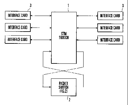
As shown in Fig. 1, the STM/Packet hybrid
switch comprises an STM switch 1 for performing
switching processing of an STM frame, a packet switch 2
for fragmenting an STM frame received from the STM
switch 1 into channels, extracting packets, and then
performing switching processing for each packet, and a
plurality of interface cards 3 for performing interface
operation between the outside of the apparatus and the
STM switch 1.
The interface cards 3 include an STM interface
card for containing data of an STM format, a PoS
interface card for containing data of PoS (Packet over
Sonet), and an Ethernet interface card for containing
data of an Ethernet format.
In Fig. 1, three interface cards 3 are
arranged on each of the input and output sides. However,
the interface card 3 is attached to each I/O port of the
STM switch 1, and the number of interface cards 3 is not
limited to three.
When the STM/Packet hybrid switch shown in
Fig. 1 is to operate as an STM switch in this
- 4 -
CA 02369449 2002-01-24
arrangement, an STM frame input to the input-side
interface card 3 is output to an output-side interface
card 3 corresponding to a transmission destination via
the STM switch 1.
When the STM/Packet hybrid switch shown in
Fig. 1 is to operate as a packet switch, an STM frame
input to the input-side interface card 3 is transferred
from the STM switch 1 to the packet switch 2. The
packet switch 2 fragments the STM frame into channels
and executes switching processing for each packet. The
packets having undergone switching processing are
constructed into an STM frame again, input to the STM
switch 1, and output to an interface card 3
corresponding to a transmission destination.
The packet switch 2 will be explained in
detail with reference to Fig. 2. As shown in Fig. 2,
the packet switch 2 comprises STM terminating units (STM
TRM) 11 for performing terminating processing of STM
frames output from the STM switch 1, channel data
extracting circuits (CH DET) 12 for distributing data of
byte-multiplexed STM frames for the respective channels,
packet detecting units (Packet DET) 13 for extracting
packets from the channel data distributed for the
respective channels, a packet switching unit (Packet
switch) 14 for performing switching processing of the
packets extracted by the packet detecting units 13, STM
mapping units (STM Mapper) 15 for distributing the
- 5 -
CA 02369449 2002-01-24
packets output from the packet switching unit 14 to
corresponding TSs (Time Slot) of STM frames, and STM
framer units (STM FRM) 16 which reassemble STM frames
from the packets distributed by the STM mapping units 15
and serve as interfaces with the STM switch 1.
Fig. 2 shows an arrangement for containing STM
frames of two ports, but the number of ports in the
packet switch 2 is not limited to two. The STM
terminating units 11, channel data extracting circuits
12, packet detecting units 13, STM mapping units 15, and
STM framer units 16 are arranged in correspondence with
the respective I/0 ports of the packet switching unit 14.
The operation of the STM/Packet hybrid switch
having this arrangement will be explained. An STM frame
output from the STM switch 1 is received by the STM
terminating unit 11 of the packet switch 2 and subjected
to terminating processing. Output data from the STM
terminating unit 11 is distributed by the channel data
extracting circuit 12 for the respective channels (or in
units of virtual concatenations), and the packets of
each channel are extracted by the packet detecting unit
13.
The packets extracted by the packet detecting
unit 13 are switched to ports corresponding to their
transmission destinations by the packet switching unit
14. Data of respective channels output from the packet
switching unit 14 are mapped into an STM format by the
- 6 -
CA 02369449 2002-01-24
STM mapping unit 15, and reassembled into an STM frame
by the STM framer unit 16. The resultant STM frame is
output to the STM switch 1.
The channel data extracting circuit 12
according to the first embodiment of the present
invention will be described in detail with reference to
Fig. 3. As shown in Fig. 3, the channel data extracting
circuit 12 comprises a Banyan unit 21 for distributing
byte-multiplexed input data for the respective channels,
a data control unit 22 for controlling input data
distribution processing of the Banyan unit 21, a
plurality of buffer units 23 for holding data of
respective channels output from the Banyan unit 21, and
a data selecting unit 24 for sequentially reading out
the data held by the buffer units 23 and outputting them.
If an STM frame contained in the STM/Packet
hybrid switch shown in Fig. 1 has a high-speed band
(e.g., 2.4 Gbps), the channel data extracting circuit 12
receives word data whose speed is converted into a low
one by parallel conversion (e.g., 38 Mbps x 8 bytes
parallel).
The data control unit 22 receives a frame
pulse representing the start of a frame signal at the
same time as input of the word data to the Banyan unit
21. By using the frame pulse as a reference, the data
control unit 22 manages a channel to which byte data of
a given TS (Time Slot) belongs, and controls input data
- 7 -
CA 02369449 2002-01-24
distribution processing of the Banyan unit 21 for each
byte.
The Banyan unit 21 is constituted by n-plane
Banyan switches (to be described later), and each plane
corresponds to a channel or a channel defined by virtual
concatenation. The Banyan switches are made up of a
plurality of 2 x 2 switches, extract channel data
fragmented into a plurality of TSs (Time Slots) for each
channel, and sequentially align the data.
When the Banyan unit 21 receives
parallel-converted data, it causes the Banyan switches
arranged for respective channels to execute switching
processing in accordance with a control signal that is
transmitted by the data control unit 22 and represents a
channel to which each byte data belongs. In this case,
each Banyan switch sets byte data belonging to its own
channel to valid byte data, and byte data belonging to
another channel to invalid byte data. The Banyan switch
performs switching processing by using only byte data
belonging to its own channel as valid byte data.
The outputs of the Banyan switches have
temporary accumulation buffers (to be described later)
for performing first-in first-out operation. Byte data
of respective channels having undergone virtual
concatenation are sequentially accumulated in the
temporary accumulation buffers. Output data from the
temporary accumulation buffers are held by the buffer
- 8 -
CA 02369449 2002-01-24
units 23, sequentially read out by the data selecting
unit 24, and output to the subsequent packet detecting
unit 13.
The arrangement of one plane of the Banyan
switch in the Banyan unit shown in Fig. 3 will be
explained with reference to Fig. 4. In the Banyan
switch shown in F.ig. 4, 8-byte parallel data are
input/output.
As shown in Fig. 4, the Banyan switch has a
Banyan management unit 31 for controlling the
transmission destination of byte data, a Banyan network
32 comprised of a plurality of multistage-connected 2 x
2 switches 34, and a plurality of temporary accumulation
buffers 33 for temporarily accumulating valid byte data
after switching processing. In Fig. 4, the Banyan
network 32 is constituted by connecting three stages of
four 2 x 2 switches 34. The structure of the Banyan
network 32 is not limited to this, and may be
constituted by multistage-connecting a larger number of
2 x 2 switches 34.
The temporary accumulation buffers 33 are
formed from a plurality of buffers for temporarily
accumulating byte data output from the Banyan network 32,
and arranged for respective bytes. In the example of
Fig. 4, the temporary accumulation buffers 33 are
constituted by eight buffers corresponding to outputs
"0" to "7" because of 8 output bytes. The Banyan
- 9 -
CA 02369449 2002-01-24
network 32 transmits input byte data to a corresponding
buffer of the temporary accumulation buffer 33 via a
root determined by the Banyan management unit 31.
The Banyan management unit 31 determines a
temporary accumulation buffer 33 serving as the
transmission destination of valid byte data Dv on the
basis of a control signal CB representing a channel to
which each byte data transmitted from the data control
unit 22 belongs.
In the example shown in Fig. 4, outputs "0" to
"4" of the temporary accumulation buffers 33 have
already held valid byte data Dv. Valid byte data Dv
input to the top position (input "0" in Fig. 4) of the
Banyan management unit 31 is assigned to output "5" of
the temporary accumulation buffer 33. Similarly, valid
byte data Dv to input "2" is assigned to output "6";
valid byte data Dv to input "6", to output "7"; and
valid byte data Dv to input "7", to output "0". Invalid
byte data DINV to inputs "3" to "5" are discarded by the
Banyan management unit 31 without being transmitted to
the temporary accumulation buffer 33.
Word data (bytes) at outputs "0" to "7"
fragmented into channels are simultaneously read out at
a predetermined timing, sequentially aligned, and output.
Referring back to Fig. 3, word data of
respective channels output from the Banyan unit 21 are
held by the buffer units 23, and sequentially output to
- 10 -
CA 02369449 2002-01-24
the subsequent packet detecting unit 13 via the data
selecting unit 24.
Note that the Banyan network 32 does not cause
internal blocking as far as input data are sequentially
sorted like packets inserted into an STM frame, as
described in "ATM Beginner's Guide: Passport to
Multimedia Age", Yokogawa Digital Computer Corp., SI
Business Division, pp. 47 - 51, July 1994.
Fig. 5 shows a state in which byte-multiplexed
data input to the channel data extracting circuit 12 are
distributed for the respective channels. As shown in
Fig. 5, byte data TSO to TSn input in response to a
frame pulse serving as a reference are assigned their
channel information, and distributed for the respective
channels by the channel data extracting circuit 12.
By using Banyan switches of planes
corresponding to channels, data are extracted for each
channel and sequentially aligned as word data (byte
data). Even data as a combination of arbitrary channels
by virtual concatenation can undergo switching
processing. In particular, the Banyan network is
adopted for word data alignment processing, so that the
channel data extracting circuit can easily cope with
virtual concatenation using a combination of any TSs,
and can suppress an increase in circuit scale.
(Second Embodiment)
Fig. 6 shows a channel data extracting circuit
- 11 -
CA 02369449 2002-01-24
according to the second embodiment of the present
invention. The channel data extracting circuit of the
second embodiment is different from that of the first
embodiment in that packet detecting units 25 are
interposed between a Banyan unit 21 and buffer units 23.
As for the remaining arrangement, the same reference
numerals as in the first embodiment denote the same
parts, and a description thereof will be omitted.
Each packet detecting unit 25 analyzes word
data distributed for the respective channels by the
Banyan unit 21, detects the boundary of a packet, and
transmits to a data control unit 22 information (e.g.,
packet length information) representing the boundary of
the next packet.
Accordingly, the data control unit 22 can
recognize start byte data of a packet for each channel.
The data control unit 22 outputs a signal representing
the start byte data of the packet to the Banyan unit 21,
and controls the Banyan unit 21 so as to output the
corresponding byte data at the start of word data, as
shown in Fig. 7.
As shown in Fig. 7, in the second embodiment,
idle data is inserted after the final byte of a packet,
and byte data at the start of the packet is always
positioned at the start of word data. This facilitates
subsequent processing. In performing this processing,
idle data is inserted after the final word of a packet.
- 12 -
CA 02369449 2002-01-24
For this purpose, the write speed to the buffer unit
must be set higher than the input data speed.
As has been described above, the present
invention achieves the following effects.
Banyan switches of planes corresponding to
channels are employed. Data are extracted in units of
channels by the Banyan switches, and sequentially
aligned in units of words. Even data as a combination
of arbitrary channels by virtual concatenation can
undergo switching processing.
Especially, the Banyan network is adopted for
data alignment processing in units of words. The
channel data extracting circuit can easily cope with
virtual concatenation using a combination of any time
slots, and can suppress an increase in circuit scale.
Data extracted for each channel is analyzed to
detect the boundary of a packet inserted into a frame.
A control signal representing whether data is start data
of the packet is generated based on the boundary of the
packet. Start data is output in accordance with the
control signal so as to be positioned at the start of
word data which constitutes the packet. Start byte data
of a packet is always positioned at the start of word
data, which facilitates subsequent processing.
- 13 -