Note: Descriptions are shown in the official language in which they were submitted.
CA 02369505 2001-10-12
WO 00/62097 PCT/SE00/00628
RADIATION DETECTOR, AN APPARATUS FOR USE IN PLANAR BEAM
RADIOGRAPHY AND A METHOD FOR DETECTING IONIZING RADIATION
FIELD OF THE INVENTION
The invention relates to a detector for detection of ionizing
radiation according to the preamble of claim 1, to an
apparatus for use in planar beam radiography according to the
preamble of claim 25 and to a method for detecting ionizing
radiation according to the preamble of claim 29.
BACKGROUND OF THE INVENTION AND RELATED ART
A detector and an apparatus of the kind mentioned above are
described in the copending PCT-application PCT/SE98/01873,
which is incorporated herein by reference. The detector
described in the reference includes a gaseous parallel plate
avalanche chamber. The detector provides good resolution, high
X-ray detection efficiency, and possibility to count every
photon absorbed in the detector. This gives further a huge
amount of possibilities when processing the detection signals,
such as energy detection, discriminating detection signals
from photons in certain energy ranges or from photons incident
at certain distance ranges from the anode or the cathode.
When using a detector of this kind in planar beam X-ray
radiography, e.g. slit or scan radiography, an apparatus which
provides that an object to be imaged only needs to be
irradiated with a low dose of X-ray photons is achieved, while
an image of high quality is obtained.
CA 02369505 2001-10-12
WO 00/62097 PCT/SE00/00628
2
Another detector and apparatus of the kind mentioned above, in
the section field of the invention, is disclosed in EP-A1-0
810 631.
For gaseous parallel plate avalanche chambers it has been
regarded as necessary that the avalanche anode and cathode
plates are parallel, and much effort has been made to achieve
high parallelism between the plates. However, the critical
point is that the distance where the electrons are subjected
to avalanche amplification, i.e. the length of the electron
avalanches, do not differ at different locations in the
gaseous parallel plate avalanche chamber. The reason for this
is that the amplification is strongly dependent on the
distance from the starting point to the end point of the
avalanche. However, avalanche anodes and cathodes have large
dimensions, in the planes they extend, compared with the
distance between them. Therefore, it has been very complicated
and costly to obtain a sufficient uniformity of those
distances or gaps.
SUMMARY OF THE INVENTION
A main object of the invention is to provide a one-dimensional
detector for detection of ionizing radiation, which employs
avalanche amplification, and provides well defined avalanches,
and which can be manufactured in a simple and cost effective
way.
This and other objects are attained by a detector according to
claim 1.
By the features of claim 1 is also achieved a detector which
can be given a length, in the direction of the incoming
CA 02369505 2001-10-12
WO 00/62097 PCT/SE00/00628
3
radiation, for achieving a desired stopping power, which makes
it possible to detect a major portion of the incoming
radiation.
By the features of claim 1 is also achieved a detector in
which electrons released by interactions between photons and
gas atoms can be extracted in a direction essentially
perpendicular to the incident radiation. Hereby it is possible
to obtain a very high position resolution.
By the features of claim 1 is also achieved a detector which
can provide good resolution, high X-ray detection efficiency,
and count a major portion of the photons incident in the
detector.
A detector which can give good energy resolution for X-rays is
also obtained.
It is also achieved a detector, which can operate at high X-
ray fluxes without performance degradation and has a long
lifetime.
By the features of claim 1 is also achieved a detector for
effective detection of any kind of radiation, including
electromagnetic radiation as well as incident particles,
including elementary particles.
It is also an object of the invention to provide an apparatus
for use in planar beam radiography, comprising at least one
one-dimensional detector for detection of ionizing radiation,
which employs avalanche amplification, provides well defined
CA 02369505 2001-10-12
WO 00/62097 PCT/SE00/00628
4
avalanches, and can be manufactured in a simple and cost
effective way.
This and other objects are attained by an apparatus according
to claim 25.
By the features of claim 25 is also achieved an apparatus for
use in planar beam radiography, e.g. slit or scan radiography,
which can provide that an object to be imaged only needs to be
irradiated with a low dose of X-ray photons, while an image of
high quality is obtained.
It is also achieved an apparatus for use in planar beam
radiography, in which a major fraction of the X-ray photons
incident on the detector can be detected, for further counting
or integration in order to obtain a value for each pixel of
the image.
It is also achieved an apparatus for use in planar beam
radiography, in which image noise caused by radiation
scattered in an object to be examined is strongly reduced.
It is also achieved an apparatus for use in planar beam
radiography, in which image noise caused by the spread of X-
ray energy spectrum is reduced.
It is also achieved an apparatus for use in planar beam
radiography, including a simple and inexpensive detector that
can operate with high X-ray detection efficiency and with good
energy resolution for X-rays.
Further is also achieved an apparatus for use in planar beam
radiography, including a detector which can operate at high X-
CA 02369505 2001-10-12
WO 00/62097 PCT/SE00/00628
ray fluxes without a performance degradation and has a long
lifetime.
It is also an object of the invention to provide a method for
5 detection of ionizing radiation, which employs avalanche
amplification, provides well defined avalanches, and can be
implemented in a simple and cost effective way.
This and other objects are attained by an apparatus according
to claim 29.
By the features of claim 29 is also achieved a method with
which it possible to detect a major portion of the incoming
radiation.
By the features of claim 29 is also achieved a method in which
electrons released by interactions between photons and gas
atoms are extracted in a direction perpendicular to the
incident radiation. Hereby it is possible to obtain a very
high position resolution.
It is also achieved a method, which can be used at high X-ray
fluxes.
BRIEF DESCRIPTION OF THE DRAWINGS
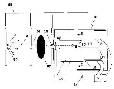
Figure 1 illustrates schematically, in an overall view, an
apparatus for planar beam radiography, according to a general
embodiment of the invention.
CA 02369505 2001-10-12
WO 00/62097 PCT/SE00/00628
6
Figure 2a is a schematic, partly enlarged, cross sectional
view, taken at II-II in Figure 1, of a detector according to a
first specific embodiment of the invention.
Figure 2b is a schematic, partly enlarged, cross sectional
view, taken at II-II in Figure 1, of a detector according to a
second specific embodiment of the invention.
Figure 2c is a schematic, partly enlarged, cross sectional
view, taken at II-II in Figure 1, of a detector according to a
third specific embodiment of the invention.
Figure 3 is a schematic view of an embodiment of an X-ray
source and an electrode formed by readout strips.
Figure 4 is a schematic top view of a second embodiment of an
X-ray source and an electrode formed by segmented readout
strips.
Figure 5 is a schematic cross sectional view of an embodiment
according to the invention, with stacked detectors.
Figure 6 is a schematic cross sectional view of a further
embodiment according to the invention, with stacked detectors.
DESCRIPTION OF PREFERRED EMBODIMENTS
Fig. 1 is a sectional view in a plane orthogonal to the plane
of a planar X-ray beam 9 of an apparatus for planar beam
radiography, according to the invention. The apparatus
includes an X-ray source 60, which together with a first thin
collimator window 61 produces a planar fan-shaped X-ray beam
9, for irradiation of an object 62 to be imaged. The first
CA 02369505 2001-10-12
WO 00/62097 PCT/SE00/00628
7
thin collimator window 61 can be replaced by other means for
forming an essentially planar X-ray beam, such as an X-ray
diffraction mirror or an X-ray lens etc. The beam transmitted
through the object 62 enters a detector 64. Optionally a thin
slit or second collimator window 10, which is aligned with the
X-ray beam forms the entrance for the X-ray beam 9 to the
detector 64. A major fraction of the incident X-ray photons
are detected in the detector 64, which includes a conversion
and drift volume 13, and means for electron avalanche
amplification 17, and is oriented so that the X-ray photons
enter sideways between two electrode arrangements 1, 2,
between which an electric field for drift of electrons and
ions in the conversion and drift volume 13 is created.
In this application planar X-ray beam is a beam that is
collimated, e.g. by collimator 61.
The detector and its operation will be further described
below. The X-ray source 60, the first thin collimator window
61, the optional collimator window 10 and the detector 64 are
connected and fixed in relation to each other by certain means
65 for example a frame or support 65. The so formed apparatus
for radiography can be moved as a unit to scan an object,
which is to be examined. In a single detector system, as shown
in Fig. 1, the scanning can be done by a pivoting movement,
rotating the unit around an axis through for example the X-ray
source 60 or the detector 64. The location of the axis depends
on the application or use of the apparatus, and possibly the
axis can also run through the object 62, in some applications.
It can also be done in a translative movement where the
detector and the collimator are moved, or the object to be
imaged is moved. In a multiline configuration, where a number
of detectors are stacked, as will be explained later, in
CA 02369505 2001-10-12
WO 00/62097 PCT/SE00/00628
8
connection with Figs. 5 and 6, the scanning can be done in
various ways. In many cases it can be advantageous if the
apparatus for radiography is fixed and the object to be imaged
is moved.
The detector 64 includes a first drift electrode arrangement
being a cathode plate 2 and a second drift electrode
arrangement being an anode plate 1. They are mutually parallel
and the space in between includes a thin gas-filled gap or
region 13, being conversion and drift volume, and an electron
avalanche amplification means 17. Alternatively the plates are
non-parallel. A voltage is applied between the anode plate 1
and the cathode plate 2, and one or several voltages is (are)
applied on the electron avalanche amplification means 17. This
results in a drift field causing drift of electrons and ions
in the gap 13, and electron avalanche amplification fields in
the electron avalanche amplification means 17. In connection
with the anode plate 1 is an arrangement 15 of read-out
elements for detection of electron avalanches provided.
Preferably the arrangement of read-out elements 15 also
constitutes the anode electrode. Alternatively the arrangement
of read-out elements 15 can be formed in connection with the
cathode plate 2 or the electron avalanche amplification means
17. It can also be formed on the anode or cathode plate
separated from the anode or cathode electrode by a dielectric
layer or substrate. In this case it is necessary that the
anode or cathode electrode is semi-transparent to induced
pulses, e.g. formed as strips or pads. In connection with
Figs.3 and 4 below different possible arrangements 15 of read-
out elements are shown.
As seen, the X-rays to be detected are incident sideways on
the detector and enters the conversion and drift volume 13
CA 02369505 2001-10-12
WO 00/62097 PCT/SE00/00628
9
between the cathode plate 2 and the anode plate 1. The X-rays
enter the detector preferably in a direction parallel to the
cathode plate 2 and the anode plate 1, and may enter the
detector through a thin slit or collimator window 10. In this
way the detector can easily be made with an interaction path
long enough to allow a major fraction of the incident X-ray
photons to interact and be detected. In the case a collimator
is used, this should preferably be arranged so that the thin
planar beam enters the detector close to the electron
avalanche amplification means 17 and preferably parallel
therewith.
The gap or region 13 is filled with a gas, which can be a
mixture of for example 90% krypton and 10% carbon dioxide or a
mixture of for example 80% xenon and 20% carbon dioxide. The
gas can be under pressure, preferably in a range 1 - 20 atm.
Therefore, the detector includes a gas tight housing 91 with a
slit entrance window 92, through which the X-ray beam 9 enters
the detector. The window is made of a material, which is
transparent for the radiation, e.g. Mylar~, or a thin aluminum
foil. This is a particularly advantageous additional effect of
the invention, detecting sideways incident beams in a gaseous
avalanche chamber 64, compared to previously used gaseous
avalanche chambers, which were designed for radiation incident
perpendicular to the anode and cathode plates, requiring a
window covering a large area. The window can in this way be
made thinner, thus reducing the number of X-ray photons
absorbed in the window.
In operation, the incident X-rays 9 enter the detector through
the optional thin slit or collimator window 10, if present,
close to the electron avalanche amplification means 17, and
CA 02369505 2001-10-12
WO 00/62097 PCT/SE00/00628
travel through the gas volume in a direction preferably
parallel with the electron avalanche amplification means 17.
Each X-ray photon produces a primary ionization electron-ion
pair within the gas as a result of interaction with a gas
5 atom. This production is caused by photoeffect, Compton-effect
or Auger-effect. Each primary electron 11 produced looses its
kinetic energy through interactions with new gas atoms,
causing further production of electron-ion pairs (secondary
ionization electron-ion pairs). Typically between a few
10 hundred and thousand secondary ionization electron-ion pairs
are produced from a 20 keV X-ray photon in this process. The
secondary ionization electrons 16 (together with the primary
ionization electron 11) will drift towards the electron
avalanche amplification means 17 due to the electric field in
the conversion and drift volume 13. When the electrons enter
regions of focused field lines of the electron avalanche
amplification means 17 they will undergo avalanche
amplification, which will be described further below.
The movements of the avalanche electrons and ions induce
electrical signals in the arrangement 15 of read-out elements
for detection of electron avalanches. Those signals are picked
up in connection with the electron avalanche amplification
means 17, the cathode plate 2 or the anode plate 1, or a
combination of two or more of said locations. The signals are
further amplified and processed by readout circuitry 14 to
obtain accurate measurements of the X-ray photon interaction
points, and optionally the X-ray photon energies.
Figure 2a shows a schematic, partly enlarged, cross sectional
view, taken at II-II in Figure 1, of a detector according to a
first specific embodiment of the invention. As seen, the
cathode plate 2 comprises a dielectric substrate 6 and a
CA 02369505 2001-10-12
WO 00/62097 PCT/SE00/00628
11
conductive layer 5 being a cathode electrode. The anode 1
comprises a dielectric substrate 3 and a conductive layer 4
being an anode electrode. Between the gap 13 and the anode 1
an electron avalanche amplification means 17 is arranged. This
amplification means 17 includes an avalanche amplification
cathode 18 and an avalanche amplification anode 19, separated
by a dielectric 24. This could be a gas or a solid substrate
24 carrying the cathode 18 and the anode 19, as shown in the
figure. As seen, the anode electrodes 4 and 19 are formed by
the same conductive element. Between the cathode 18 and the
anode 19 a voltage is applied by means of a DC power supply 7
for creation of a very strong electric field in an avalanche
amplification region 25. The avalanche region 25 is formed in
a region between and around the edges of the avalanche cathode
18 which are facing each other, where a concentrated electric
field will occur due to the applied voltages. The DC power
supply 7 is also connected with the cathode electrode 5 and
the anode electrode 4 (19). The voltages applied are selected
so that a weaker electric field, drift field, is created over
the gap 13. Electrons (primary and secondary electrons)
released by interaction in the conversion and drift volume 13
will drift, due to the drift field, towards the amplification
means 17. They will enter the very strong avalanche
amplification fields and be accelerated. The accelerated
electrons 11, 16 will interact with other gas atoms in the
region 25 causing further electron-ion pairs to be produced.
Those produced electrons will also be accelerated in the
field, and will interact with new gas atoms, causing further
electron-ion pairs to be produced. This process continues
during the travel of the electrons in the avalanche region
towards the anode 19 and an electron avalanche is formed.
After leaving the avalanche region the electrons will drift
towards the anode 19. Possibly the electron avalanche
CA 02369505 2001-10-12
WO 00/62097 PCT/SE00/00628
12
continues up to the anode 19 if the electric field is strong
enough.
The avalanche region 25 is formed by an opening or channel in
the cathode 18 and the dielectric substrate 24, if present.
The opening or channel can be circular, seen from above, or
continuous, longitudinal extending between two edges of the
substrate 24, if present, and the cathode 18. In the case the
openings or channels are circular when seen from above they
are arranged in rows, each row of openings or channels
including a plurality of circular openings or channels. A
plurality of longitudinal openings or channels or rows of
circular channels are formed beside each other, parallel with
each other or with the incident X-rays. Alternatively, the
circular openings or channels can be arranged in other
patterns.
The anode electrodes 4, 19 also forms readout elements 20 in
the form of strips provided in connection with the openings or
channels forming the avalanche regions 25. Preferably one
strip is arranged for each opening or channel or row of
openings or channels. The strips could be divided into
sections along its length, where one section could be provided
for each circular opening or channel or for a plurality of
openings or channels, in the form of pads. The strips and the
sections, if present, are electrically insulated from each
other. Each detector electrode element i.e. strip or section
is preferably separately connected to processing electronics
14. Alternatively the read-out elements can be located on the
back side of the substrate (opposite the side of the anode
electrodes 4, 19). In this case it is necessary that the anode
electrodes 4, 19 are semi-transparent to induced pulses, e.g.
in the form of strips or pads. In connection with Figs.3 and 4
CA 02369505 2001-10-12
WO 00/62097 PCT/SE00/00628
13
below different possible arrangements 15 of read-out elements
are shown.
As an example the longitudinal channels can have a width in
the range 0.01-1 mm, the circular channels can have a diameter
of the circle being in the range 0.01-1 mm, and the thickness
of the dielectric 24 (separation between the avalanche cathode
18 and anode 19) is in the range 0.01-1 mm.
Alternatively the conductive layers 5, 4 can be replaced by a
resistive carrier of e.g. silicon monoxide, conductive glass
or diamond, with the dielectric substrates 3, 6 replaced by a
conductive layer. In such a case a dielectric layer or carrier
is preferably arranged between the conductive layer and the
readout elements 20 when they are located in connection with a
drift electrode arrangement.
Figure 2b shows a schematic, partly enlarged, cross sectional
view, taken at II-II in Figure 1, of a detector according to a
second specific embodiment of the invention. This embodiment
differs from the embodiment according to Figure 2a in that the
anode electrodes 4 and 19 are formed by different conductive
elements, being spaced by a dielectric, which could be solid
or a gas, and that the openings or channels also are formed in
the avalanche anode electrode 19. The avalanche amplification
anode 19 is connected to the DC power supply 7. In the case
the dielectric between the anode electrodes 4 and 19 is solid,
it includes openings or channels through the dielectric, the
openings or channels essentially corresponding the openings or
channels forming the avalanche regions 25. An electric field
is created between the anode electrodes 4 and 19. This field
could be a drift field, i.e. a weaker field, or an avalanche
amplification field, i.e. a very strong electric field. In
CA 02369505 2001-10-12
WO 00/62097 PCT/SE00/00628
14
connection with Figs.3 and 4 below different possible
arrangements 15 of read-out elements are shown.
Figure 2c shows a schematic, partly enlarged, cross sectional
view, taken at II-II in Figure 1, of a detector according to a
third specific embodiment of the invention. The detector
includes a cathode 2, as described above, an anode 1, and an
avalanche amplification means 17. A gap 13 being a conversion
and drift volume is provided between the cathode 2 and the
avalanche amplification means 17. The gap 13 is gas filled and
the cathode 2 is formed as described above. The drift anode 1
is provided on a back surface of a dielectric substrate 26,
e.g. a glass substrate. On the front surface of the substrate
26, avalanche amplification cathode 18 and anode 19 strips are
alternately provided. The cathode 18 and anode 19 strips are
conductive strips, and are connected to the DC power supply 7,
for creation of a concentrated electric field, i.e. an
avalanche amplification field in each region between a cathode
strip 18 and an anode 19 strip. The anode 1 and cathode 2 are
also connected to the DC power supply 7. The voltages applied
are selected so that a weaker electric field, drift field, is
created over the gap 13. Alternatively the dielectric
substrate 26 can be replaced by a gas. The anodes and the
cathodes are then supported, e.g. in their respective ends.
Preferably the avalanche anode strips 19 also forms the read
out elements 20, and are then connected to the processing
electronics 14. The avalanche cathode strips 18 could instead
form the read out elements, or together with the anode strips
19. As an alternative the anode electrode 1 can be constituted
of strips, which can be segmented, and being insulated from
each other. Those strips could then form the read out elements
alone or together with the anode and/or cathode strips. The
CA 02369505 2001-10-12
WO 00/62097 PCT/SE00/00628
strips acting as anode/cathode and read out element are
connected to the DC power supply 7 and the processing
electronics 14, with appropriate couplings for separation. In
a further alternative the cathode strips 18 and/or the anode
5 strips 19 are formed by an underlying conductive layer covered
by a resistive top layer, made of e.g. silicon monoxide,
conductive glass or diamond. This reduces the power of
possible sparks, which could appear in the gas due to the
strong electric field. In a further alternative of an
10 arrangement of read out strips the read out strips 20 are
arranged under and parallel with the avalanche anode strips
19. The read out strips 20 are then made a little wider than
the avalanche anode strips 19. If they are located under the
anode 1 it is necessary that the anode electrode is semi-
15 transparent to induced pulses, e.g. in the form of strips or
pads. In yet another alternative the anode 1 can be omitted
since the necessary electric fields can be created by means of
the cathode electrodes 5, 18 and the anode electrodes 19.
As an example, the glass substrate is about 0.1- 5 mm thick.
Further, the conductive cathode strip has a width being about
20-1000 ~.m and the conductive anode strip has a width being
about 10-200 Vim, with a pitch of about 50-2000 Vim. Cathodes and
anodes can be divided into segments along their extension.
In operation, X-ray photons enter the space 13 in the detector
of Fig. 2c essentially parallel with the avalanche cathode 18
and anode 19 strips. In the conversion and drift volume 13 the
incident X-ray photons are absorbed and electron-ion pairs are
produced as described above. A cloud of primary and secondary
electrons, being the result of interactions caused by one X-
ray photon drift towards the avalanche amplification means 17.
CA 02369505 2001-10-12
WO 00/62097 PCT/SE00/00628
16
The electrons will enter the very strong electric field in the
gas filled region between an anode strip and a cathode strip,
which is an avalanche amplification region. In the strong
electric field the electrons initiate electron avalanches. As
a result the number of electrons which is collected on the
anode strips is of a few orders of magnitude higher than the
number of primary and secondary electrons (so called gas
multiplication). One advantage with this embodiment is that
each electron avalanche only induces a signal mostly on one
anode element or essentially on one detector electrode
element. The position resolution in one coordinate is
therefore determined by the pitch.
In the embodiments described above different locations for the
detector electrode arrangements have been described. There are
many variations, e.g. more than one detector electrode
arrangement can be provided, adjacent to each other with
different directions of the strips or segments, or at separate
locations.
Referring to Fig. 3, a possible configuration of a detector
electrode arrangement 4, 5, 15, is shown. The electrode
arrangement 4, 5, 15 is formed by strips 20', and can also act
as anode or cathode electrode as well as detector electrode. A
number of strips 20' are placed side by side, and extend in
directions parallel to the direction of an incident X-ray
photon at each location. The strips are formed on a substrate,
electrically insulated from each other, by leaving a space 23
between them. The strips may be formed by photolithographic
methods or electroforming, etc. The space 23 and the width of
the strips 20' are adjusted to the specific detector in order
to obtain the desired (optimal) resolution. In for example the
embodiment of Figure 2a the strips 20' should be placed under
CA 02369505 2001-10-12
WO 00/62097 PCT/SE00/00628
17
the openings or channels or rows of openings or channels and
have essentially the same width as the openings or channels,
or somewhat wider. This is valid for both the case that the
detector electrode arrangement is located separated from the
anode electrode 4 and for the case the detector electrode
arrangement also constitutes the anode electrode 4.
Each strip 20' is connected to the processing electronics 14
by means of a separate signal conductor 22, where the signals
from each strip preferably are processed separately. Where an
' anode or cathode electrode constitutes the detector electrode,
the signal conductors 22 also connects the respective strip to
the high voltage DC power supply 7, with appropriate couplings
for separation.
As seen from the figure, the strips 20' and the spacings 23
aim at the X-ray source 60, and the strips grow broader along
the direction of incoming X-ray photons. This configuration
provides compensation for parallax errors.
The electrode arrangement shown in Fig. 3 is preferably the
anode, but alternatively or conjointly the cathode can have
the described construction. In the case the detector electrode
arrangement 15 is a separate arrangement, the anode electrode
4 can be formed as a unitary electrode without strips and
spacings. The same is valid for the cathode electrode or the
anode electrode, respectively, when only the other thereof
comprises the detector electrode arrangement. However, if the
detector electrode arrangement is located on a substrate on
the opposite side to a cathode or anode electrode, the anode
or cathode electrode is semi-transparent to induced pulses,
e.g. formed as strips or pads.
CA 02369505 2001-10-12
WO 00/62097 PCT/SE00/00628
18
In Fig. 4, an alternative configuration of an electrode is
shown. The strips have been divided into segments 21,
electrically insulated from each other. Preferably a small
spacing extending perpendicular to the incident X-rays is
provided between each segment 21 of respective strip. Each
segment is connected to the processing electronics 14 by means
of a separate signal conductor 22, where the signals from each
segment preferably are processed separately. As in Fig. 3,
where the anode or cathode electrode constitute the detector
electrode, the signal conductors 22 also connects the
respective strip to the high voltage DC power supply 7.
This electrode can be used when the energy of each X-ray
photon is to be measured, since an X-ray photon having higher
energy statistically causes a primary ionization after a
longer path through the gas than an X-ray photon of lower
energy. By means of this electrode, both the position of X-ray
photon interaction and the energy of each X-ray photon can be
detected. By statistical methods one can restore the spectrum
of the incident photons with very high energy resolution. See
for example E. L. Kosarev et al., Nucl. Instr and methods 208
(1983)637 and G. F. Karabadjak et al., Nucl. Instr and methods
217 (1983)56.
Generally for all embodiments, each incident X-ray photon
causes one induced pulse in one (or more) detector electrode
element. The pulses are processed in the processing
electronics, which eventually shapes the pulses, and
integrates or counts the pulses from each strip (pad or sets
of pads) representing one pixel. The pulses can also be
processed so as to provide an energy measure for each pixel.
CA 02369505 2001-10-12
WO 00/62097 PCT/SE00/00628
19
Where the detector electrode is on the cathode side the area
of an induced signal is broader (in a direction perpendicular
to the direction of incidence of the X-ray photons) than on
the anode side. Therefore, weighing of the signals in the
processing electronics is preferable.
Fig. 5 shows schematically an embodiment of the invention with
a plurality of the inventive detectors 64 stacked, one on top
of another. By this embodiment multiline scan can be achieved,
which reduces the overall scanning distance, as well as the
scanning time. The apparatus of this embodiment includes an X-
ray source 60, which together with a number of collimator
windows 61 produce a number of planar fan-shaped X-ray beams
9, for irradiation of the object 62 to be imaged. The beams
transmitted through the object 62 optionally enters the
individual stacked detectors 64 through a number of second
collimator windows 10, which are aligned with the X-ray beams.
The first collimator windows 61 are arranged in a first rigid
structure 66, and the optional second collimator windows 10
are arranged in a second rigid structure 67 attached to the
detectors 64, or arranged separately on the detectors.
The X-ray source 60, the rigid structure 66, and the possible
structure 67 including collimator windows 61, 10,
respectively, and the stacked detectors 64, which are fixed to
each other, are connected and fixed in relation to each other
by a certain means 65 e.g. a frame or support 65. The so
formed apparatus for radiography can be moved as a unit to
scan an object, which is to be examined. In this multiline
configuration, the scanning can be done in a transverse
movement, perpendicular to the X-ray beam, as mentioned above.
It can also be advantageous if the apparatus for radiography
is fixed and the object to be imaged is moved.
CA 02369505 2001-10-12
WO 00/62097 PCT/SE00/00628
A further advantage of using a stacked configuration, compared
to large single volume gas detectors, is reduction of
background noise caused by X-ray photons scattered in the
5 object 62. These scattered X-ray photons travelling in
directions not parallel to the incident X-ray beam could cause
"false" signals or avalanches in one of the other detectors 64
in the stack, if passing through anode and cathode plates and
entering such a chamber. This reduction is achieved by
10 significant absorption of (scattered) X-ray photons in the
material of the anode and the cathode plates, or the
collimator 67.
This background noise can be further reduced by providing thin
15 absorber plates 68 between the stacked detectors 64, as shown
in Fig. 6. The stacked detector is similar to that of Fig. 5,
with the difference that thin sheets of absorbing material is
placed between each adjacent detectors 64. These absorber
plates or sheets can be made of a high atomic number material,
20 for example tungsten.
As an alternative for all embodiments, the electric field in
the conversion and drift gap (volume) can be kept high enough
to cause electron avalanches, hence to be used in a pre-
amplification mode.
It is general for all embodiments that the gas volumes are
very thin, which results in a fast removal of ions, which
leads to low or no accumulation of space charges. This makes
operation at high rate possible.
It is also general for all embodiments that the small
distances leads to low operating voltages, which results in
CA 02369505 2001-10-12
WO 00/62097 PCT/SE00/00628
21
low energy in possible sparks, which is favorable for the
electronics.
The focusing of the field lines in the embodiments is also
favorable for suppressing streamer formations. This leads to a
reduced risk for sparks.
As a further alternative embodiment the gap or region 13 may
include an ionizable medium such as a liquid medium or a solid
medium instead of said gaseous medium. Said solid or liqula
medium may be a conversion and drift volume and an electron
avalanche volume.
The liquid ionizable medium may for instance be THE (Tri
Methyl Ethane) or TMP (Tri Methyl Pentane) or other liquid
ionizable media with similar properties.
The solid ionizable medium may for instance be a semi
conducting material, for instance silicon or germanium. When
the ionizable medium is solid a housing around the detector
can be excluded.
Detectors using the solid or liquid ionizable medium can be
much thinner, and they are less sensitive to the direction of
the incident X-rays with respect to the resolution of the
image from the radiated object detected by the detector, than
similar gaseous detectors.
The electric field is preferably in the region to cause
avalanche amplification but the invention will also work at
lower electrical field range, i.e. not high enough to cause
electron avalanches when using solid or liquid ionizable media
in the detector.
CA 02369505 2001-10-12
WO 00/62097 PCT/SE00/00628
22
Although the invention has been described in conjunction with
a number of preferred embodiments, it is to be understood that
various modifications may still be made without departing from
the spirit and scope of the invention, as detinec~ ny Lne
appended claims. For example the voltages can be applied in
other ways as long as the described electrical fields are
created.