Language selection

Search

Patent 2369688 Summary

Third-party information liability

Some of the information on this Web page has been provided by external sources. The Government of Canada is not responsible for the accuracy, reliability or currency of the information supplied by external sources. Users wishing to rely upon this information should consult directly with the source of the information. Content provided by external sources is not subject to official languages, privacy and accessibility requirements.

Claims and Abstract availability

Any discrepancies in the text and image of the Claims and Abstract are due to differing posting times. Text of the Claims and Abstract are posted:

  • At the time the application is open to public inspection;
  • At the time of issue of the patent (grant).
(12) Patent: (11) CA 2369688
(54) English Title: CONTACT ASSEMBLY FOR A PLUG CONNECTOR, IN PARTICULAR FOR A PCB PLUG CONNECTOR
(54) French Title: ENSEMBLE DE CONTACTS POUR CONNECTEUR ENFICHABLE, EN PARTICULIER POUR CONNECTEUR ENFICHABLE DE CARTE IMPRIMEE
Status: Deemed expired
Bibliographic Data
(51) International Patent Classification (IPC):
  • H01R 12/71 (2011.01)
  • H01R 12/55 (2011.01)
  • H01R 13/502 (2006.01)
  • H05K 3/34 (2006.01)
  • H01R 43/24 (2006.01)
  • H01R 12/14 (2006.01)
(72) Inventors :
  • PAPE, GUNTER (Germany)
  • KOHLER, ANDREAS (Germany)
(73) Owners :
  • HARTING ELECTRONICS GMBH & CO. KG (Germany)
(71) Applicants :
  • HARTING KGAA (Germany)
(74) Agent: SMART & BIGGAR IP AGENCY CO.
(74) Associate agent:
(45) Issued: 2004-10-12
(22) Filed Date: 2002-01-30
(41) Open to Public Inspection: 2002-08-05
Examination requested: 2002-01-30
Availability of licence: N/A
(25) Language of filing: English

Patent Cooperation Treaty (PCT): No

(30) Application Priority Data:
Application No. Country/Territory Date
101 05 042.9 Germany 2001-02-05

Abstracts

English Abstract

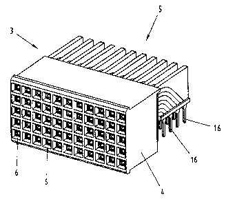
The invention relates to a contact carrier for a plug connector, in particular for a PCB plug connector. The contact carrier comprises a carrier body which is made of plastics, and a plurality of contacts which are accommodated in the carrier body and each have two plug-in portions and one transition portion located between the two plug-in portions. The transition portions are exposed at least in part and the carrier body is provided with thermally conductive webs which are located between the transition portions and adjoin the latter.


French Abstract

L'invention concerne un support de contact pour une fiche de connexion, en particulier pour une fiche de connexion de carte CI. Le support de contact comprend un corps de contact qui est en matière plastique, et une pluralité de contacts qui sont placés dans le support de contact et qui présentent chacun deux parties enfichables et une partie de transition située entre les deux parties enfichables. Les parties de transition sont exposées au moins partiellement et le corps de support est muni de barrettes thermoconductrices qui sont situées entre les parties de transition et adjacentes à ces dernières.

Claims

Note: Claims are shown in the official language in which they were submitted.


-6-

Claims

1. A contact carrier for a plug connector, in particular for a PCB plug
connector, said contact carrier comprising a carrier body which is made of
plastics, and a plurality of contacts which are accommodated in said carrier
body
and each have two plug-in portions and one transition portion located between
said two plug-in portions, said transition portions being exposed at least in
part,
said carrier body being provided with thermally conductive webs which are
located between said transition portions and adjoin the latter.

2. The contact carrier as claimed in claim l, wherein on an outside of said
carrier body said thermally conductive webs terminate flush with said
transition
portions.

3. The contact carrier as claimed in claim 1, wherein on an outside of said
carrier body said thermally conductive webs are connected with each other by
at
least one reinforcing web which extends transverse to said transition
portions.

4. The contact carrier as claimed in claim 1, wherein said carrier body has a
reinforcing edge which is thicker than said thermally conductive webs.

5. The contact carrier as claimed in claim 4, wherein said carrier body has a
holding web which is thicker than said thermally conductive webs, said
reinforcing edge being separated from said holding web by a circulation
passage.

6. The contact carrier as claimed in claim l, wherein in a region of an exit
from said carrier body said contacts are surrounded by injection-molding for
about 270°.

Description

Note: Descriptions are shown in the official language in which they were submitted.


CA 02369688 2002-O1-30
H 1745 CA
A Contact Assembly for a Plug Connector, in particular for a PCB Plug
Connector
S
Technical Field
This invention relates to a contact assembly for a plug connector, in
particular
for a PCB plug connector.
Background of the Invention
A generic contact assembly is known from European Patent 0 422 785. Such
assembly comprises a carrier body which is made of plastics, and a plurality
of
contacts which are accommodated in the carrier body and each have two plug-in
portions and one transition portion located between the two plug-in portions.
The
transition portions are exposed at least in part. The contacts are embedded
within
the carrier body by injection-molding. In the interior of the carrier body a
recess is
provided, through which the transition portions of the contacts freely extend.
By
appropriately choosing the exposed length of the transition portions, an
impedance matching is to be achieved.
In some applications it may be desirable to mount a plug connector, equipped
with the above-mentioned contact assemblies, on a printed circuit board by
means
of a reflow soldering method. In this method, a solder is applied onto the
printed
circuit board. Subsequently, the printed circuit board equipped with the plug
connector is heated in an oven, so that the solder melts and the plug-in
portions,
which constitute contact pins and are plugged into the printed circuit board,
are
soldered to the printed circuit board.
In this method it is problematic that all contact pins must be heated as
uniformly as possible, in order to obtain a consistently high quality of the
soldered
connection in all contact pins. It was found out that in the known contact
assemblies a consistently good heating of the contacts is not ensured.


CA 02369688 2002-O1-30
-2-
Brief Summary of the Invention
It is the object of the invention to improve a contact assembly as mentioned
above such that a rather uniform and quick heating of all contacts is ensured.
This is achieved in a contact assembly comprising a carrier body which is
made of plastics, and a plurality of contacts which are accommodated in the
carrier body and each have two plug-in portions and one transition portion
located
between the two plug-in portions. The transition portions are exposed at least
in
part and the Garner body is provided with thermally conductive webs which are
located between the transition portions and adjoin the latter. The invention
is
IO based on the finding that the air between the transition portions, which is
present
in prior art contact assemblies, acts as insulator and prevents a uniform
heating of
the contact pins. The thermally conductive webs primarily serve to uniformly
distribute the heat between the various contacts. Since via their transition
portion
the longer contacts of a contact assembly basically absorb more heat than the
shorter contacts, there is obtained a temperature gradient between the
contacts.
This temperature gradient is leveled out by the 'thermally conductive webs. In
addition, the thermally conductive webs offer a large heat-exchanging surface
for
the warm air in the oven, which heat-exchanging surface approximately is as
large
as the exposed surface of the transition portions. This provides for a faster
heating
of the contacts, which provides for short process times. A positive side
effect of
the thermally conductive webs finally is the fact that they stabilize the
carrier
body. To provide for a free circulation of the air between the contact
assemblies
during reflow soldering, said carrier body is made as thin as possible;
therefore,
an additional stabilization is welcome.
The principle underlying the invention can be expressed in other words as
follows: The carrier body of the contact assembly is made very thin, namely
with
a thickness which corresponds to the thickness of the transition portions of
the
contacts. The result is that the contacts are exposed on the outsides of the
carrier
body. The thickness of the carrier body is larger than the distance of
adjacent
contact columns. The result is that between the individual carrier bodies a


CA 02369688 2002-O1-30
-3-
comparatively large distance exists, so that the warm air in the oven can
easily
- circulate between the carrier bodies.
In accordance with a preferred embodiment of the invention it is provided that
on an outside of the carrier body the thermally conductive webs terminate
flush
with the transition portions. This allows an unhindered circulation of the
heated
air between adjacent contact assemblies.
In accordance with the preferred embodiment of the invention it is furthermore
provided that on an outside of the carrier body the thermally conductive webs
are
connected with each other by at least one reinforcing web which extends
transverse to the transition portions. The reinforcing web. stabilizes the
thermally
conductive webs, so that the same cannot bulge or even buckle under an axial
load
acting on the contact assembly, as it may occur for instance when mounting the
contact assemblies.
Preferably, it is provided that the carrier body has a reinforcing edge which
is
IS thicker than the thermally conductive webs, and that the carrier body has a
holding web which is likewise thicker than the thermally conductive webs, the
reinforcing edge being separated from the holding web by a circulation
passage.
Both the reinforcing edge and the holding web increase the mechanical strength
of
the carrier body, and they are exactly arranged in those regions in which
forces
acting on the plug-in portions of the contacts must be introduced into the
carrier
body. The circulation passage serves to specifically heat that contact which
has
the shortest transition portion and therefore always is the slowest to heat
up,
namely the contact at the transition between holding web and reinforcing edge.
In accordance with an alternative embodiment of the invention it may be
provided that the contacts in the region of the exit from the carrier body are
surrounded by injection-molding for about 270°. It was found out that
to firmly
anchor the contacts in the carrier body it is not necessary to completely
embed the
contact by injection-molding; thus, material can be saved.
Advantageous aspects of the invention can be taken from the sub-claims.


r
CA 02369688 2002-O1-30
-4-
Brief Description of the Drawings
- Figure 1 shows a perspective, schematic view of a PCB plug connector
which is equipped with contact assemblies according to the invention;
- Figure 2 shows a perspective view of a contact assembly according to the
invention;
- Figure 3 shows another perspective view of the contact assembly of Figure 2;
and
- Figure 4 shows a section along plane N-IV of Figure 3.
Detailed Description of the Preferred Embodiments
Figure 1 shows a PCB plug connector 3 which has a housing 4 as well as a
plurality of contact assemblies 5 inserted in the housing such that they are
arranged with a small spacing parallel to each other and one beside the other.
For
each contact assembly, the housing has a column 6 of contact openings into
which
the contacts of a complementary plug connector can be plugged.
In the embodiment shown in the Figures, each contact assembly (see Figures 2
to 4) has five contacts 12 which each have two plug-in portions 14, 16 as well
as
one transition portion 18. The plug-in portions 14 constitute contact springs
which
are disposed in the housing 4 behind the contact openings. The plug-in
portions 16
constitute contact pins which can be plugged into a printed circuit board (not
shown in the Figures). Since the contact springs and the contact pins extend
at an
angle of 90° with respect to each other, this type of plug connector is
also referred
to as angled plug connector.
The contacts of a contact assembly are accommodated in a carrier body 20
which is made of plastics and roughly has the shape of a flat cuboid. In the
region
of the transition from the contact springs 14 to the transition portions 18,
the
carrier body is provided with a thickened holding web 22. The same ensures a
sufficient mechanical strength on the side of the contact assembly facing a


CA 02369688 2002-O1-30
-5-
complementary plug connector. Adjoining the holding web 22 a substantially
flat
middle portion 24 of the carrier body is disposed.
The middle portion 24 is provided with thermally conductive webs 26 which
between each other have free spaces in which the transition portions of the
contacts are disposed. The thermally conductive webs are as thick as the
transition
portions and adjoin the latter. As can be seen in Figure 3, the thermally
conductive
webs terminate flush with the transition portions, so that this side of the
middle
portion 24 is flat with the exception of a reinforcing edge 28, which is
formed
adjacent the contact pins 16. The reinforcing edge 28 terminates at a distance
from
the holding web 22, so that a circulation passage 30 is formed, which provides
for
an improved circulation of air along the otherwise flat side of the middle
portion
24. The circulation passage is disposed precisely in the region of the contact
with
the shortest transition portion, so that this contact is heated specifically.
On the side of the middle portion 24 to be seen in Figure 2, the reinforcing
edge 28 is formed continuously. Between the upper edge and the lower edge in
this Figure two reinforcing webs 32 are formed, which are integrally connected
with the thermally conductive webs 26. The reinforcing webs 28 serve as
contact
surface for the transition portions 18 of the contacts.
In Figure 2, an alternative embodiment is indicated in broken lines, in which
grooves 34 are spared in the reinforcing edge 28 and in the holding web 22 in
the
region of the exit of the contacts from the carrier body; thus, the contacts
are
surrounded by injection-molding in this region only for about 270°.
This design
leads to a saving of material and a further improved circulation of air.
Apart from the good circulation of air along the outsides of the contact
assembly, the above-described design has another advantage: Since the middle
portion is made very thin, namely with the same thickness as the transition
portions of the contacts, the volume of plastic material, which must be heated
during soldering together with the contacts, is minimized. This ensures a
rather
uniform heating within a rather short period.

Representative Drawing
A single figure which represents the drawing illustrating the invention.
Administrative Status

For a clearer understanding of the status of the application/patent presented on this page, the site Disclaimer , as well as the definitions for Patent , Administrative Status , Maintenance Fee  and Payment History  should be consulted.

Administrative Status

Title Date
Forecasted Issue Date 2004-10-12
(22) Filed 2002-01-30
Examination Requested 2002-01-30
(41) Open to Public Inspection 2002-08-05
(45) Issued 2004-10-12
Deemed Expired 2018-01-30

Abandonment History

There is no abandonment history.

Payment History

Fee Type Anniversary Year Due Date Amount Paid Paid Date
Request for Examination $400.00 2002-01-30
Registration of a document - section 124 $100.00 2002-01-30
Application Fee $300.00 2002-01-30
Maintenance Fee - Application - New Act 2 2004-01-30 $100.00 2004-01-08
Registration of a document - section 124 $100.00 2004-05-20
Final Fee $300.00 2004-07-16
Maintenance Fee - Patent - New Act 3 2005-01-31 $100.00 2004-12-20
Maintenance Fee - Patent - New Act 4 2006-01-30 $100.00 2005-12-20
Maintenance Fee - Patent - New Act 5 2007-01-30 $200.00 2006-12-18
Maintenance Fee - Patent - New Act 6 2008-01-30 $200.00 2007-12-20
Maintenance Fee - Patent - New Act 7 2009-01-30 $200.00 2008-12-15
Maintenance Fee - Patent - New Act 8 2010-02-01 $200.00 2009-12-23
Maintenance Fee - Patent - New Act 9 2011-01-31 $200.00 2010-12-23
Maintenance Fee - Patent - New Act 10 2012-01-30 $250.00 2011-12-15
Maintenance Fee - Patent - New Act 11 2013-01-30 $250.00 2012-12-18
Maintenance Fee - Patent - New Act 12 2014-01-30 $250.00 2013-12-11
Maintenance Fee - Patent - New Act 13 2015-01-30 $250.00 2015-01-07
Maintenance Fee - Patent - New Act 14 2016-02-01 $250.00 2016-01-06
Owners on Record

Note: Records showing the ownership history in alphabetical order.

Current Owners on Record
HARTING ELECTRONICS GMBH & CO. KG
Past Owners on Record
HARTING KGAA
KOHLER, ANDREAS
PAPE, GUNTER
Past Owners that do not appear in the "Owners on Record" listing will appear in other documentation within the application.
Documents

To view selected files, please enter reCAPTCHA code :


To view images, click a link in the Document Description column. To download the documents, select one or more checkboxes in the first column and then click the "Download Selected in PDF format (Zip Archive)" or the "Download Selected as Single PDF" button.

List of published and non-published patent-specific documents on the CPD .

If you have any difficulty accessing content, you can call the Client Service Centre at 1-866-997-1936 or send them an e-mail at CIPO Client Service Centre.


Document
Description 
Date
(yyyy-mm-dd) 
Number of pages   Size of Image (KB) 
Cover Page 2004-09-16 1 47
Abstract 2002-01-30 1 15
Description 2002-01-30 5 259
Claims 2002-01-30 1 39
Drawings 2002-01-30 4 106
Representative Drawing 2002-04-08 1 18
Cover Page 2002-07-12 1 46
Assignment 2002-01-30 5 164
Prosecution-Amendment 2003-08-27 1 29
Assignment 2004-05-20 3 136
Correspondence 2004-07-16 1 34