Note: Descriptions are shown in the official language in which they were submitted.
CA 02370359 2002-02-O1
1
SEMICONDUCTOR LASER MODUhE AND FIBIgR AMPLIFIER AND
OPTICAL COMMUNICATIONS SYSTEM USING THE SAME
BACKGROUND
Field of the Invention
The present invention relates to a~ semiconductor
laser module designed as a pumping source for an optical
communications system. More particularly, the invention
relates to a complex cavity type semiconductor laser module
which has a Fabry-Perot semiconductor laser device
optically coupled to an optical feedback part, such as a
fiber Bragg grating (FBG), a dielectric multilayered filter
or a distribution Bragg reflector (DBR). This module is
useful as a laser module which has a characteristic of
emitting a pumping laser beam with a high optical output, a
laser module which has a characteristic of emitting'a
pumping laser beam with an optical stability or a pumping
source which has a suppressed occurrence of kinks and is
used in, for example, a wavelength division multiplexing
system that employs a Raman amplification system.
Wavelength division multiplexing (WDM) communications
systems have been developed as optical communications
systems that transmit a plurality of signal lights. In
such a system, optical amplifiers are arranged at
predetermined locations in an optical path and a laser
module incorporating a Fabry-Perot semiconductor laser
device is connected to each optical amplifier. As a
pumping laser beam having a predetermined oscillation
spectrum is input to each optical amplifier from the laser
module, the optical signal that has been attenuated in the
transmission through the upstream path is amplified and the
optically amplified signal light is transmitted again to
CA 02370359 2002-02-O1
2
the downstream path.
At present, an Er-doped fiber amplifier (EDFA) is
widely used as an optical amplifier in that system
The EDFA executes optical amplification of a
stimulated emission type. That is, Er ions are excited by
a pumping laser beam which is input from the laser module
and a flat gain wavelength bandwidth defined at the energy
level appears in the EDFA. The signal light of the
wavelength that is included in the flat gain wavelength
bandwidth is optically amplified.
In the EDFA, the practical gain wavelength bandwidth
which is concerned with the optical amplification of signal
light or the flat gain wavelength bandwidth is about 1530
to 1610 nm; That is, in case where optical signal
amplified in the system is limited to the one whose
wavelength lies within the aforementioned bandwidth.
The Raman amplification system also has been known as
an optical amplification system for signal light. This
amplification system has a characteristic such that signal
light having a wider bandwidth can be optically amplified
as compared with the case of the EDFA. Therefore, there is
a growing expectation of adapting the Raman amplification
system to optical communications systems.
The Raman amplification system is an optical
amplification system which employs such a phenomenon that
as a laser beam having an extremely high optical output
(pumping laser beam) is input town optical fiber,
stimulated Raman scattering occurs in the optical fiber,
giving a gain at a frequency smaller by 13 THz than the
wavelength of the pumping laser beam (on the longer
wavelength side by approximately 100 nm), and as signal
light of a wavelength included in the wavelength bandwidth
that provides the gain is input to the optical fiber a.n
such a pumped state, the signal light is optically
CA 02370359 2002-02-O1
3
amplified.
Unlike the EDFA system; the Raman amplification
system can be directly adapted to existing optical paths
because the system can use an optical fiber (optical path)
itself as an amplification medium without using a special
optical fiber. That is, unlike the EDFA system, the Raman
amplification system can reduce relay points in the entire
optical paths. This can simplify the maintenance and
control of the entire system and reduce. the construction
cost and maintenance cost of the entire:.system while
improving the reliability of the entire. system.
In principle, the Raman amplification system can
optically amplify signal light of an arbitrary wavelength
bandwidth because the system can provide a gain at a
frequency smaller by 13 THz than the wavelength of a
pumping laser beam of an arbitrary wavelength by varying
the wavelength of a pumping laser beam to be input to an
optical fiber, i.e., by inputting the pumping laser beam to
the optical fiber.
In case where the Raman amplification system is
adapted to the WDM communications system, therefore, it is
possible to increase the number of channels of signal
lights.
In the case of the Raman amplification system, the
gain of an optical fiber has a certain wavelength
distribution. In case where a pumping laser beam shows an
oscillation spectrum having the center wavelength at 1430
nm, for example, the gain that is realized in the Raman
amplification has a peak in the vicinity of the wavelength
of 1530 nm and has an asymmetrical gain distribution with a
margin of about 20 nm around the peak wavelength.
To realize a flat gain over a wide wavelength
bandwidth, therefore, the Raman amplification system
multiplexes a plurality of pumping laser beams whose center
CA 02370359 2002-02-O1
4
wavelengths and optical outputs have been adjusted and
inputs the multiplexed laser beam to an optical fiber.
Specifically, as a plurality of pumping laser beams
whose center wavelengths differ from one another are output
from a plurality of laser modules and are multiplexed by a
wavelength multiplexing coupler and the wavelength-
multiplexed single pumping laser beam is input to the
optical fiber, the gains of the individual pumping laser
beams are made to continuously overlap one another on the
long wavelength side of about 100 nm, thereby realizing a
gain of a wide wavelength bandwidth on the whole.
In case where a pumping laser beam of, for example,
100 mW is input to an existing communications optical fiber
from a laser module, the obtained Raman gain is about 3 dB,
which is too small to adequately realize optical
amplification of signal light.
In view of the above, the Raman amplification system
is demanded to generally use a pumping laser beam with a
high optical output of 200 mW or greater, preferably 300 mW
or greater and more preferably 400 mW to 1 W, in order to
acquire a gain which can ensure optical amplification of
signal light:
In general, therefore, an optical output with the
desired intensity is acquired by multiplexing laser beams
from a plurality of laser modules and inputting the'
multiplexed laser beam to an optical fiber as a pumping
laser beam:
As apparent from the above, the adlaptation of the
Raman amplification system to the WDM communications system
has several advantages. However, laser modules as a
pumping source in the Raman amplification system have many
problems to solve.
The essential characteristics of which a Raman
amplification pumping source are demanded will be discussed
CA 02370359 2002-02-O1
as follows.
(1) First, a laser module which is a pumping source
should emit a very hsgh optical output. Specifically, as
mentioned earlier, an optical output of 200 mW or greater
5 should be emitted. A general system multiplexes laser
beams from a plurality of laser modules. This requires not
only that the multiplexed optical output as a whole should
become high power but also that the individual laser
modules should emit high outputs.
(2) When the center wavelength of the pumping laser
beam from a laser module varies, the wavelength bandwidth
of the Raman gain varies: As a result, it causes a
mismatch between the wavelength bandwidth of the Raman gain
and the wavelength of signal light to be optically
amplified. This makes it difficult to realize the intended
optical amplification. In the WDM commmnications system,
particularlg, when such a gain variation occurs, the
flatness of the gasp wavelength bandwidth is impaired.
This makes it difficult to realize stable optical
amplification of signal light over a wide bandwidth.
The laser module is therefore demanded of an
excellent wavelength stability to emit a pumping laser beam
with a small variation in center wavelength. Specifically,
the demanded laser module should be able to emit a pumping
laser beam whose variation in center wavelength lies within
1 nm under the driving conditions of the ambient
temperature of 0 to 70°C and the driving current of 0 to 1
A.
(3) In case where the intensity of the pumping laser
beam varies (fluctuates) in the Raman amplification system,
the Raman gain fluctuates, lowering the: signal to noise
ratio (S/N ratio} of signal light. In this respect, the
pumping laser beam from the laser module should be
noiseless.
CA 02370359 2002-02-O1
6
There are three pumpyg systems for Raman
amplification: forward pumping system, backward pumping
system and bidirectional pumping system. At present, the
backward pumping system is a mainstream for the following
reason. In the case of the forward pumping system in which
a low-power signal light and a high-poorer pumping laser
beam travel in the same direction, the signal light, is
significantly affected by the variation (fluctuation) of
the intensity of the pumping laser beam. This brings about
a difficulty in the system reliability.
Even if a laser module is used as a forward pumping
source, therefore, there still is a demand for development
of a laser module which does not cause a variation in the
intensity of a pumping laser beam and has an excellent
i5 optical stability.
(4) Raman amplification is realized when the
polarization direction of signal light matches with, the
polarization direction of the pumping laser beam. That is,
Raman amplification has a polarization dependency. To
achieve Raman amplification, therefore, it is necessary to
reduce the influence of a difference beaween the
polarization direction of signal light and the polarization
direction of the pumping laser beam:
In this case, if the backward pumping system is used
for Raman amplification, the polarization direction of
signal light becomes at random during propagation so that
the polarization dependency is curbed.
As the forward pumping system makers the polarization
dependency of Raman amplification stronger, however, the
system requires that the pumping laser beam in use should
reduce the polarization dependency of R.aman amplification.
This makes it necessary to perform depolarization on the
pumping la er beam to thereby reduce the degree of
polarization (DOP).
CA 02370359 2002-02-O1
7
In case where a plurality of laser modules are
optically coupled to a wavelength multiplexing coupler to
acquire a high-power pumping laser beam, is required as
follows.
The ratio of the power of a laser beam from each
laser module which lies in the pass band of the wavelength
multiplexing coupler to the entire power should be equal to
or greater than a predetermined value, specifically, for
example, 90°s or higher, and the ratio should be stable
while the laser module is driven.
In consideration of the fact that the pumping laser
beam from the laser module has an oscillation spectrum
formed by plural Fabry-Perot modes; the degree of the width
of the oscillation spectrum is an important factor to
fulfill the requirement.
If the width of the oscillation spectrum becomes too
wide, the number of Fabry-Perot modes present in the width
of the oscillation spectrum becomes large; so that at the
time of driving the laser module, the power distribution
among the Fabry-Perot modes varies to the level at which
noise or a variation in gain cannot be neglected. In
addition, the multiplexing loss at the time of multiplexing
the wavelengths by the wavelength multiplexing coupler
becomes large. If the width of the oscillation spectrum
becomes too narrow, on the other hand, it becomes difficult
to reduce the polarization dependency of the Raman gain and
a kink occurs in the current v.s. optical output
characteristic of the laser module, thus limiting the
optical output of the laser module.
The "width of the oscillation spectrum" mentioned
here is a wavelength bandwidth that provides a spectral
intensity lower by 3 dB than a peak value in the waveform
of the pumping laser beam from the laser module.
In view of the above, the width of the oscillation
CA 02370359 2002-02-O1
8
spectrum should be 3 nm or narrower, preferably 2 nm or
narrower. Thus, the pumping laser beam is required to have
smaller degree of polarization and the width of the
oscillation spectrum of 3 nm or narrower. It is known that
the degree of polarization of a multimode pumping laser
beam which has at least three Fabry-Perot modes, preferably
four to five; in the width of the oscillation spectrum
becomes smaller.
Therefore, the laser module that 3.s used when the
Roman amplification system is adapted to the WDM
communications system should meet the requirement that the
width of the oscillation spectrum is 3 nm or narrower and a
multimode pumping laser beam which has at least three
Fabry-Perot modes in the width of the oscillation spectrum
should be emitted.
The use of a multimode pumping la~:er beam is
advantageous in making it difficult to cause a reduction in
the pumping efficiency based on the stimulated Brillouin
scattering which occurs when a high optical output
concentrates in a narrow wavelength bandwidth. In this
case, the preferable spacing between the Fabry-Perot modes
of the pumping laser beam is said to be. 0.1 nm or larger.
OBJECT AND SUMMARY OF THE hNVENTION
Accordingly, it is an object of tree present invention
to provide a semiconductor laser module: which emits a laser
beam having an extremely high optical output and an
excellent wavelength stability.
It is another object of the preserut invention to
provide a semiconductor laser module which is useful as a
pumping source in the WDM communications system to which
the Roman amplification system is adapted.
It is a further object of the present invention to
provide a fiber amplifier which uses the semiconductor
CA 02370359 2002-02-O1
9
laser module and an optical communications system which
uses the fiber amplifier.
To achieve the above object, according to one aspect
of the present invention, there is provided a following
semiconductor laser module (module A).
The module A comprises:
a Fabry-Perot semiconductor laser device to a front
facet of which an optical feedback part having a wavelength
selectivity and showing a specific reflectivity with
respect to a specific wavelength is optically coupled,
wherein given that a cavity length of the
semiconductor laser device is L (unit: ~.m), a reflectivity
of the front facet is R1 ( % ) and a peak reflectivity of the
optical feedback part is RZ ( % ) , following equations are
satisfied among L, R1 and R2
1000 ~,m s L s 3500 ~,m ( 1 ) " and
0.010 s R1 + czR? s 4% (2)
where c represents a coupling efficiency between the
semiconductor laser device and the optical feedback part.
A preferred module A satisfies the. relationships
represented by the following expressions:
1000 ~,m s L s 3500 ~.m ( 1 ) ,, and
0.1% s Rl + c2R2 s 4% (2' ;I .
According to another aspect of the. present invention,
there is provided a following semiconductor laser module
(module B).
The module B comprises:
a Fabry-Perot semiconductor laser device to a front
facet of which an optical feedback part having a wavelength
selectivity and showsng a specific reflectivity with
respect to a specific wavelength is optically coupled,
wherein given that a cavity length of the
semiconductor laser device is L (unit: ~;m), a reflectivity
of the front facet is R1 ( % ) and a peak reflectivity of the
CA 02370359 2002-02-O1
optical feedback part is RZ (%), following equations are
satisfied among L, Rx and RZ
1000 ~,m s L s 3500 ~.m ( 1 ) " and
Rl/R2 s 0 . 8 ( 3 ) ,.
5 According to a further aspect of the present
invention, there is provided a following semiconductor
laser module (module C).
The module C comprises:
a Fabry-Perot semiconductor laser device to a front
10 facet of which an optical feedback part having a wavelength
selectivity and showing a specific reflectivity with
respect to a specific wavelength is optically coupled,
wherein given that a cavity length of the
semiconductor laser device is L (unit: hum), a reflectivity
of the front facet is R1 ( % ) and a peak reflectivity of the
optical feedback part is RZ (%); following equations are
satisfied among L, R1 and Rz
1000 ~,m s L s 3500 ~.m ( 1 ) "
0 . 01 % s R1 + c2Rz s 4
(2)" and
R1/RZ s 0 . 8 ( 3 )
where c represents a coupling efficiency between the
semiconductor laser device and the optical feedback part.
A preferred module C satisfies the. relationships
represented by the following expressions:
1000 ~.m s L s 3500 ~.m ( 1 ) ,,
0 .1% s Rl + c2R2 s 4% ( 2 ' ;I , and
Rl/Rz s 0 . 8 ( 3 ) ..
Further, with respect to all of th.e modules A, B and
C according to the present invention, the optical feedback
part may be designed to have a reflection bandwidth ~~, (nm)
meeting the following condition:
0.2 nm s ~~, s 3 nm (4),
thus providing as a more suitable optical module.
CA 02370359 2002-02-O1
11
According to the present invention, there are
provided a fiber amplifier which a es one of the modules A,
B and C as a pumping source and an optical communications
system which has the fiber amplifier and one of the modules
A, B and C.
BRIEF DBSCRIPTION OF THE DRAWINGS
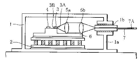
Fig. l is a schematic diagram showing one example of
a laser module according to the present invention;
Fig. 2 is an exemplary diagram illustrating the state
in which a semiconductor laser device and a fiber Bragg
grating which are essential components of the laser module
are optically coupled to each other;
Fig. 3 is a cross-sectional view along the lime III-
III in Fig. 2;
Fig. 4 is a graph showing the relationship among the
cavity length (L) of the semiconductor laser device, the
reflectivity ( R1 ) of a front facet and a maximum optical
output (Pmax);
Fig. 5 is a graph showing the relationship among the
cavity length (L) of the semiconductor laser device, the
reflectivity (R1) of the front facet and the maximum
optical output (Pmax);
Fig. 6 is an explanatory diagram for explaining the
power in band of the laser module;
Fig. 7 is a graph showing the results of Experiment
II;
Fig. 8 is a graph showing the relationship between
the reflectivity ( Rl ) of the front facet of a semiconductor
laser device in a laser module C of the present invention
and the peak reflectivity (R2) of a fiber Bragg grating;
and
Fig. 9 is a graph showing the current v.s. optical
output characteristics of Example l and Example 2.
CA 02370359 2002-02-O1
12
DETAILED DESCRIPTION
To begin with, the thought process to develop a
module according to the present invention will be discussed.
In the process of devoting to study to achieve the
objects, the present inventors paid attention to the fact
that, as already disclosed in WO 00/46893, a Fabry-Perot
semiconductor laser device having a cavity length set to
1000 ~m or greater could provide a high optical output if
optimized by reducing the reflectivity of the front facet
(output facet): To aim at producing a semiconductor laser
module for Raman amplification that is demanded of a high
optical output of 200 mW or greater, the present inventors
reached the conclusion that the aforementioned Fabry-Perot
semiconductor laser device with a long cavity length should
be used as a laser device (light source) to be incorporated
in the semiconductor laser module.
The results of measuring the maximum optical outputs
of a laser device by changing the cavity length and the
reflectivity of the front facet showed a certain
correlation among the cavity length, the front facet
reflectivity and the maximum optical output.
With regard to the achievement of the waveleng h
stability of a pumping laser beam, the present inventors
paid attention to a method of forming a.n optical coupling
system of a complex cavity type by optically coupling the
laser device and a fiber Bragg grating. This method has
been known as a method of fixing the oscillation wavelength
of a Fabry-Perot semiconductor laser device.
In the complex cavity type optical. coupling system,
as the driving current or the ambient temperature varies,
the oscillation spectrum of the laser device changes,
resulting in a change in the center wavelength of the gain
wavelength bandwidth to be obtained. Because the mirror
CA 02370359 2002-02-O1
13
loss characteristic is lower at the vicinity of the center
wavelength of the reflection bandwidth of the fiber Bragg
grating, however, the oscillation spectrum of the laser
device is pulled into the vicinity of the center wavelength
of the reflection bandwidth of the fiber Bragg grating
(pull-in of the oscillation spectrum of the laser device)
so that the wavelength bandwidth of the laser beam emitted
from the optical coupling system or the pumping laser beam
is fixed to the vicinity of the center wavelength of the
reflection bandwidth of the fiber Bragg grating.
Studying the pull-in conditions of the oscillation
spectrum of a laser device in the complex cavity type
optical coupling system constructed by changing the
reflectivity of the front facet of the laser device and the
reflectivity of the fiber Bragg grating', the inventors
discovered that it was necessary to set the relation
between the reflectivity of the front facet of the laser
device and the reflectivity of the fiber Bragg grating to
the aforementioned relation in order to ensure the pull-in
operation. The inventors succeeded to quantify the
essential conditions for wavelength stability in terms of
the equations (1), (2), (3) and (4) and. combinations
thereof and developed the modules of th.e present invention
based on the discovery.
In the modules A, B and C; the equations (1) and (2)
are essential conditions for the complex cavity type
optical coupling system to provide a high optical output.
The equation (3) means the essential condition for pulling
the oscillation spectrum of the laser device into the
vicinity of the center wavelength of the reflection
bandwidth of the optical feedback part. As will be
discussed later, the equation (4) means the essential
condition for suppressing the occurrence of a kink
attributable to longitudinal mode hopping when the module
CA 02370359 2002-02-O1
14
is driven.
For the present, therefore, the module A functions as
a complex cavity type pumping source which emits a high
optical output.
For the'present; therefore, the module B functions as
a complex cavity type pumping source which ensures at least
the wavelength stability while being able to emit a high
optical output.
The module C that satisfies the equations (1), (2)
and (3) surely has both characteristics of providing a high
optical output and an excellent wavelength stability, and
is very useful as a pumping source of the Raman
amplification system.
Any of the modules A, B and C that: fulfill the
equation (4) demonstrates its own function mentioned above
as well as the suppressed occurrence of a kink.
Those modules can have any optical. feedback part as
long as the optical feedback part has a. wavelength
selectivity and shows a specific reflectivity with respect
to a specific wavelength. For example, a fiber Bragg
grating, a dielectric multilayered filter and a
distribution Bragg reflector (DBR) are available as'the
optical feedback part. Of those three, the fiber Bragg
grating is suitable.
The basic structure of the modules A, B and C of the
present invention is exemplified in Fig. 1. The
exemplified module uses a fiber Bragg grating as its
optical feedback part.
In Fig. l, a package 1 houses a Peltier module 2 and
a substrate 6 on which a Fabry-Perot semiconductor laser
device 3 with suppressed high-order transverse modes, as
discussed later, a thermistor 4 and lenses 5a and 5b are
secured is fixed on the Peltier module 2. An optical fzber
7 having a fiber Bragg grating 7A to be discussed later is
CA 02370359 2002-02-O1
secured into a through hole 1b formed i.n a side wall la of
the package 1.
In the modules, as a laser beam wr~ich is emitted from
a front facet 3A of the laser device 3 and has an
5 oscillation spectrum formed by a plurality of Fabry'-Perot
modes passes the two lenses 5a and 5b, the laser beam is
condensed and input to the end face of the optical fiber 7.
The laser beam is then waveguided through the core of the
optical fiber 7 and of the waveguided laser beam, the
10 Fabry-Perot mode light that is included. in the reflection
bandwidth (4~) of the fiber Bragg grating is reflected at
th8 fiber Bragg grating 7A and returns to the laser device
as a reflection light of a specific wavelength. Each
module is of a complex cavity type in which resonance
15 between the front facet 3A and a rear facet 3B of the laser
device 3 and resonance between the rear facet 3B of the
laser device 3 and the fiber Bragg grating 7A are
compounded.
It is possible to use a single lens and/or a lensed
fiber in place of the lenses 5a and 5b.
According to the modules of the present invention,
the laser beam emitted from the laser device 3 carries out
a sequence'of resonant operations in which resonance in the
cavity of the laser device 3 and resonance between the rear
facet 3B and the fiber Bragg grating 7A are compounded,
then becomes a high-power pumping laser beam and is
transmitted to a predetermined place in the optical path
from the optical fiber 7.
At the time such an operation takes place, the
driving current introduced in the laser device 3 heats up
the laser device, raising the device temperature. When the
device temperature rises, the center wavelength and the
spectral intensity in the oscillation spectrum of the
emitted laser beam vary. To prevent this shortcoming, each
CA 02370359 2002-02-O1
16
module of the present invention measurea the device
temperature with the thermistor 4 located near the laser
device 3 and the laser device 3 is adequately cooled by
regulating,the operational current of t:he Peltier module 2
under the control of an external control circuit (not
shown) using the measured value, so that the temperature of
the laser device 3 is set constant.
In the modules with the structure shown in Fig. 1,
the equations (1) and (2) are met for t:he module A, the
equations (1) and (3) are met for the module B, and the
equations (1) through (3) are met for t:he module C at the
same time.
Any one of the modules can suppress the generation of
a kink caused by longitudinal mode hopping by setting the
reflection bandwidth 0~ of the fiber Bragg grating to 3 nm
or narrower.
The optical coupling of the semiconductor laser
device 3 and the fiber Bragg grating in the module in Fig.
1 from which the other components are omitted is
illustrated as an exemplary diagram in Fig. 2.
In Fig. 2, the optical fiber 7 having the fiber Bragg
grating 7A formed therein is arranged facing the front
facet 3A of the semiconductor laser device 3, thereby
constituting the optical coupling system of the laser
device 3 and the fiber Bragg grating 7A,.
The meanings of the equations (1) through (4) will be
discussed with reference to the aboveme,ntioned optical
coupling system.
First, a description will be given of the equa ions
(1) and (2) that are essential conditions for the optical
coupling system to provide a high optical output.
The laser device 3 is the light emission source of
the optical coupling system: If emission of a high optical
output from the optical coupling system. is achieved, it
CA 02370359 2002-02-O1
17
means that the laser device 3 as the light emission source
provides a high optical output. In this respect, first it
is necessary to look for a condition for realizing the
emission of a high optical output from the laser device 3.
The semiconductor laser device 3 in the optical
coupling system is of a Fabry-Perot type one example of
which is depicted in Fig. 2 and across-sectional view of
Fig. 3 along the line III-III in Fig. 2.
The laser device 3 has a lower cladding layer 12, a
lower GRIN-SCH layer 13, an active layer 14 with a quantum
well structure and an upper GRIN-SCH layer 15 deposited in
order on a substrate 1l of a predetermined semiconductor by
a known epitaxial growth method, such as a metal organic
vapor phase epitaxial growth method, liquid phase epitaxial
method, molecular beam epitaxy, gas source molecular beam
epitaxy or chemical beam epitaxy. An upper cladding layer
16 and a cap layer 17 are laminated on the upper GRIN-SCH
layer 15. An upper electrode 18 is formed on the cap layer
17 and a lower electrode l9 is formed at the back of the
substrate 11.
A p-type layer 21 and an n-type layer 22 are
laminated on the sides of the lower cladding layer 12, the
lower GRIN-SCH layer l3, the active layer l4 and the upper
GRIN-SCH layer 15 in the named order.
And the active layer 14 is surrounded by current
blocking layer, thereby forming a realizing current ration
and suppressing high order traverse modes.
The laser device 3 is fabricated by forming a
laminated structure of a semiconductor material by a
predetermined epitaxial growth method, cleaving the
structure to a predetermined cavity length L, depositing a
low-reflectivity film on one cleaved face to form the front
facet 3A having a peak reflectivity R1 ~(g) and depositing a
high-reflectivity film on the other cleaved face to form
CA 02370359 2002-02-O1
18
the rear facet 3B.
The semiconductor material for the laser device 3 is
adequately selected in consideration of: the relation
between the material property and the designated wavelength
(center wavelength) of the pumping laser beam that is used
in an optical amplifier for signal light. In case of
acquiring a pumping laser beam having t:he designated
wavelength of 1300 to 1600 nm, for example, the laser
device 3 can be fabricated by using a material selected
from GaInAs, GaInAsP, AlGaInAs and GaIrnNAs material systems.
In such a laser device, generally speaking, the
longer the cavity length L is, the lower the series
resistance of the laser device when driven current becomes
the greater and the greater the heat dissipation area
becomes. The heat saturation phenomenon of the optical
output is restrained and a variation ins the center
wavelength of the oscillation spectrum is restrained too.
This makes it possible to increase the driving current of
the laser device, thereby ensuring a high optical output as
well as the stability of the center wavelength of the
oscillation spectrum.
However, merely making the cavity length L longer
lowers the mirror loss in the front facet 3A and the rear
facet 3B and increases the influence of the inner loss of
the cavity. This results in a reduction in an external
quantum efficiency of the laser device 3.
In view of the above, the present inventors conducted
the following experiment I and studied the relationship
among the cavity length L, the peak reflectivity Rl of the
front facet and the optical output.
Experiment I
First, the inventors fabricated various laser devices
that have a layered structure shown in Fig. 3 or a lattice
mismatched quantum well active region having both the lower
CA 02370359 2002-02-O1
19
GRIN-SCH layer 13 and the upper GRIN-SCH layer 15 formed of
non-doped GaInAsP and having the active layer 14 formed of
GaInAsP, by setting the reflectivity of the rear facet 3B
constant to 95o and changing the cavity length L and the
peak reflectivity R1 of the front facet 3A. The laser
devices were driven and the maximum optical outputs (Pmax:
mW) of the laser devices were measured. The measuring
results are illustrated in Figs. 4 and 5:
The following are apparent from Figs. 4 and 5.
1) As apparent from Fig. 4, as the cavity length L
is made longer beyond 1000 ~m with the peak reflectivity R1
of the front facet 3A set constant, the value Pmax of each
laser device increases as the cavity length L gets longer
when the value of R1 is equal to or lesa than 4%.
2) As apparent from Fig. 5, as reflectivity R1 of the
front facet 3A is increased with the cavity length L set
constant, the value Pmax of each laser device changes in
such a curve as to have a peak at a certain R1. What is
more, as the cavity length L becomes longer, the value Pmax
becomes greater but the peak of the value Pmax in each
curve varies in such a way as to become larger as the value
of R1 gets smaller.
3) In view of the above, to increase the value Pma.x
of the laser device, it is effective to make the cavity
length L longer and make the reflectivity Rl of the front
facet 3A smaller at the same time as apparent from Fig. 5.
4) In consideration of the fact that the demanded
optical output of the pumping source in the Raman
amplification system is 200 mW or higher, it is apparent
from Fig. 5 that in case of using the laser device as the
pumping source, the cavity length L should be set equal to
or greater than 1000 ~:m and the reflectivity R1 of the
front facet 3A should be set within a range of 0.01 to 4%,
more preferably 0.1 to 4~.
CA 02370359 2002-02-O1
' 20
If the cavity length L is set too long, however, the
influence of the inner loss of the cavity increases, as
mentioned above, causing a reduction in mirror loss. This
not only reduces the external quantum efficiency but causes
cracking or damage in the cavity during the formation of a
chip in the process of manufacture of the laser device 3,
which leads to a lower manufacturing yield. In view of the
above, the upper limit of the cavity length of the laser
device 3 is set to 3500 ~.m.
Considering those circumstances, ~'.n case where the
laser device that emits a high optical output of 20O mW or
higher, the cavity length L should be 1.000 to 3500 ;gym,
preferably be 3f00 ~,m or shorter where the longitudinal
mode spacing is 0.1 mm or longer, from the viewpoint of
preventing stimulated Brillouin scattering. The
reflectivity of the front facet should be set to 0.01 to 4~,
preferably 0.1 to 4%.
The module shown in Fig. 1 is a complex cavity type
having the laser device 3 optically coupled to the fiber
Bragg grating 7A. Unlike the laser device used in the
experiment I which carries out resonance between one front
facet and one rear facet, the module has resonance in the
laser device 3 compounded with resonancse between the fiber
Bragg grating 7A and the rear facet 3B of the laser device
3, resulting in the emission of the pumping laser beam from
the optical fiber 7.
Therefore, the module can be assumed as a laser
device which has a single cavity structure. In this case,
the reflectivity of the rear facet of the assumed laser
device is equivalent to the reflectivity of the rear facet
3B of the actual laser device 3. The assumed laser device
does not actually have a front facet. If the assumed laser
device had the front facet, however; the reflectivity of
the front facet can be effectively expressed by an equation
CA 02370359 2002-02-O1
21
R1 + c2Rz where R1 is the reflectivity o:E the front facet 3A
of the real laser device 3 and Rz is the peak reflectivity
of the fiber Bragg grating 7A.
By adapting the discovery made in the experiment I to
the assumed laser device or the module shown in Fig. 1, the
optical output of the module can beset: to a high optical
output of 200 mW.
In other words, on the assumption that a high optical
output of 200 mW can be provided by setting the cavity
length L of the laser device 3 as the incorporated light
emission source to 1000 ~m or longer (t:he equation (1)
satisfied), if the reflectivity R1 of the front facet 3A of
the laser device 3 and the reflectivity Rz of the fiber
Bragg grating 7A are designed in such a way that the
effective front facet reflectivity of t;he module, R1 + czR2,
to 0 . 01 °s s R1 + c2R2 s 4% , preferably 0 . 1 % s R1 + c2R2 s 4
°s ,
the maximum optical output (Pmax) of the module can show
200 mW or higher.
The equation (2) that a.s the essential condition for
the module A of the present invention i.s determined this
way.
Note that the coupling efficiency c in the equation
(2) represents the optical coupling efficiency between the
laser device and the fiber Bragg grating (optical feedback
part) and is normally set to lie in the. range of 0.75 s c
s 0.9.
Satisfying both the relationships of the equations
(1) and (2) at the same time, the module A of the present
invention can be driven as a pumping source which emits a
high-power pumping laser beam of 200 mW or higher.
The module B of the present invention will now be
discussed.
As the cavity length of the laser device 3
incorporated in the module B satisfies the equation (1),
CA 02370359 2002-02-O1
22
the module B can emit a high optical output. Satisfying
the equation (3) at the same time can provide an excellent
wavelength stability for the pumping laser beam to'be
emitted.
That is, even if the center wavelength of the
oscillation spectrum of the laser beam emitted from the
laser device 3 varies, the module B pulls in and fixes the
oscillation spectrum to the vicinity oj. the center
wavelength of the reflection bandwidth 0~, of the fiber
Bragg grating 7A and thus emits a pumping laser beam which
does not change the Raman gain when used as a pumping laser
beam having an outstanding wavelength stability or'a
pumping laser beam for Raman amplificai-ion.
The~followi.ng experiment II was conducted to find a
condition for pulling the laser beam emitted from the laser
device 3 into the vicinity of the center wavelength of the
reflection bandwidth ~~, of the fiber Bz-agg grating 7A.
Experiment II
Two types of laser devices 3 which had a cavity
length L of 1000 ~,m and whose front facets 3A had
reflectivities Rl of 1% and 4% and four types of fiber
Bragg gratings 7A which had a reflectic>n bandwidth ~~, of
1.5 nm and had peak refiectivities Ra of 1%, 3%, 5%'and 7%
were prepared and both components were adequately combined
to construct the modules shown in Fig. 1. For the
individual modules, the optical output spectra were
measured under the same conditions and the ratio (power in
band: o) of the optical output to be coupled to the
reflection bandwidth 0~, were calculated. from the wavelength
spectra of the optical outputs based on the following
specifications .
As shown_in Fig. 6, the spectral curve of the optical
output to be acquired has a peak optical output Po at the
position of the center wavelength ~,FB~ in the reflection
CA 02370359 2002-02-O1
23
bandwidth 4~, of the fiber Bragg grating 7A: To begin with,
the entire area, So, under the spectral curve is computed.
Wavelengths ~.1 and 7~1' that provide an optical output,
1/2Po, a half of the peak optical output Po, are acquired
and an area S1 of the hatched portion in the diagram which
lies between the wavelength ~.1 and the 'wavelength ~,1' a.s
computed. Then, S1 x 100/So (%) is computed as the "power
in band value".
A larger power in band value indicates that even if
the center wavelength of the oscillation spectrum of the
laser device 3 varies, the oscillation spectrum is pulled
into the vicinity of the center wavelength ~,FB~ of the
reflection bandwidth 0~, of the fiber Bragg grating 7A so
that the wavelength of the pumping laser beam emitted from
the module is stable. In other words, the fiber Bragg
grating 7A'works to effectively realize; the pull-in of the
laser beam emitted from the laser deW c;e 3.
In general, if the value of S1 x 100/So ( % ) is equal
to or greater than 60%, the pull-in operation is
effectively accomplished and the pumping laser beam from
the module has an excellent wavelength stability.
A parameter of R1/RZ was set and the relatianship
between the power in band value computed in the
aforementioned manner and R1/RZ was acquired in the
experiment II. The results are depicted in Fig. 7.
In case of the module whose R,/RZ 9Ls 0.8 or less, as
apparent from Fig. 7, the value of S1 x 100/So is equal to
or greater than 60%. That is, it is understood that the
module shown in Fig. 1 should be designed in such a way
that Ri/RZ becomes 0.8 or less in order to achieve the
pull-in of the laser beam from the laser device 3 by the
fiber Bragg grating 7A.
The module B was developed in view of the knowledge
obtained through the experiment IT. As the module
CA 02370359 2002-02-O1
24
incorporates a laser device with a lone cavity length, it
can emit a high-power pumping laser be<~m and has a
necessary condition to secure the wavelength stability of
the pumping laser beam:
The module C of the present invention satisfies a1.1
of the equations (1), (2) and (3). Because the module C
has a high power optical output of 200 mW or greater and a
capability of surely emitting a pumping laser beam with an
excellent wavelength stability, the module C is useful as a
pumping source when the Raman amplification system is
adapted.
The relationship between R1 and RZ def fined in the
equations (2) and (3) is shown in Fig. 8. The module C
that simultaneously fulfills the equations (2) and (3) can
be assembled when the values of R1 and RZ satisfy any value
lying in the hatched area in Fig. 8.
In this case, the value of R1 + c2122 given in the
equation (2) varies depending on the value of the coupling
efficiency c as c is a variable.
Therefore, the proper R1 and RZ have only to be
selected in Fig. 8 in association with the efficiency (c)
of coupling between the laser device 3 and the fiber Bragg
grating 7A as a designed value of the laser module to be
fabricated.
As shown in Fig. 5 showing the res:ults of the
experiment I, the maximum optical output Pmax of the laser
device 3 incorporated in the module varies depending on the
level of the reflectivity R1 of the front facet 3A and the
size of the cavity length L. In case where the laser
device 3 has'a cavity length L of 1300 Vim; for example,
Pmax shows a high value of 350 to 400 mW when the
reflectivity Ri of the front facet 3A is 0 . 6 to 2% . In
case where the laser device 3 has a cavity length L of 1500
~,m, Pmax shows a high value of 400 to 470 mW when the
CA 02370359 2002-02-O1
reflectivity R1 of the front facet 3A is 0.14 to 1.7°s.
That is, to acquire a high optical output as the cavity
length L is made longer, the reflectiv3.ty R1 of the front
facet of the laser device should be made lower, as apparent
5 from Fig. 5.
Therefore, in case where the laser. device 3
incorporated in the module C has a lone cavity length L,
the value of R1 + czR2 should be made small, whereas' in case
where the laser device 3 has a short caivity length L, the
10 value of Ri + c2R2 should be made large .
In case where the center wavelength of the
oscillation spectrum of the pumping laser beam from the
laser device 3 in the any of the modules A, B and C' is
pulled into the vicinity of the center wavelength of the
15 reflection bandwidth ~~, of the fiber Bragg grating 7A, the
oscillation spectral width of the laser device 3 is
included in the reflection bandwidth of the fiber Bragg
grating 7A:
In consideration of the condition: that the
20 oscillation spectral width of the laser device 3 is set to
3 nm or less, preferably 2 nm or less, in order to reduce
the degree of polarization of the pumping laser beam from
the module, suppress the generation of a kink and acquire a
pumping laser beam of multi-mode which can restrain a
25 variation in Raman gain, it is preferable to set the
reflection bandwidth O~, of the fiber Bragg grating 7A to 3
nm or less. If ~~, is made too narrow, however, the center
wavelength cannot be pulled into the reflection bandwidth
of the fiber Bragg grating 7A. It is therefore preferable
that A~, should lie in the range of 0.2 nm s ~~, s 3 nm.
With regard to the reflection bandwidth ~~, and peak
reflectivity RZ of the fiber Bragg grating 7A, the
following experiment III was conducted.
Experiment III
CA 02370359 2002-02-O1
26
Prepared was a laser device which had a cavity length
L of 1300 ~.m and whose front facet 3A had a peak
reflectivity of 1.2o and whose oscillation spectrum had a
center wavelength of 1480 nm. Also prepared were the fiber
Bragg gratings whose peak reflectivities Rz and reflection
bandwidths ~~, had values given in Table; 1. Fifteen modules
were assembled by combining the laser device and the fiber
Bragg gratings, their optical output v.s. current
characteristics were measured and it was checked whether or
not a kink occurred. The results are :shown as the
relationship between the peak reflectivity RZ and the
reflection bandwidth d~, in Table 1.
Note that the mark O in Table 1 means the generation
of no kink up to the maximum driving current, the mark
means the generation of a small kink and the mark X means
the generation of a large kink.
0~ (nm)
0.5 1.0 1.5 2.0 3.0
1 x O O O
RZ (s) 5 not measured O O O not measured
x D ~ 0 x
As apparent from Table 1, the reflection bandwidth
and the peak reflectivity RZ should be ~~ombined adequately
in order to suppress the generation of a kink. Generally
speaking, the use of the fiber Bragg grating whose peak
reflectivity R2 is 7% or less and whose reflection
bandwidth ~~, is 3 nm or narrower can allow the assembled
module to suppress the generation of a kink.
In view of the above, it is desirable to set the
reflection bandwidth O~; of the fiber Bragg grating 7A to 3
CA 02370359 2002-02-O1
27
nm or narrower, preferably 2 nm or narrower.
Examples
Two kinds of laser devices 3 were fabricated by
forming a laminated structure in Fig. 3 on the substrate
using a GaInAsP-based semiconductor material, then :cleaving
the structure so that the cavity length became 1300 ~m and
1500 ~,m, forming a high-reflectivity f3.lm: of a reflectivity
of 95~ on one cleaved face to form the rear facet 3B and
forming a low-reflectivity film of a reflectivity of 1.20
on the other cleaved face to form the front facet 3A.
Those laser devices emit laser beams with an oscillation
spectrum having a center wavelength of 1480 nm.
The specifications of the laser devices are shown in
Table 2.
Table 2
Laser Laser
Dev3.ce Device b
a
Cavity length 1300 1500
(L: N,m)
rear facet 95 95
Reflectivity (
~ ) front facet (R1) 0.1 0 ~ 1
Center wavelength 1480 1480
of oscillation
spectrum (nm)
Then,;the modules shown in Fig. 1 were assembled by
optically coupling the front facet 3A of each laser device
to the end face of the optical fiber 7 having the fiber
Bragg grating 7A formed therein. The coupling efficiency c
was 0.76 for the module with L = 1300 ~,;m and 0.85 for the
module with L = 1500 Vim.
In consideration of the results of the experiment I
given in Fig. 5 such that the reflectivity Rl of the front
facet 3A which would provide a peak in the curve of the
CA 02370359 2002-02-O1
28
maximum optical output Pmax of the laser device having the
cavity length L of 1300 ~.m was about 1.2°s and the
reflectivity R1 of the front facet 3A i:n the case of the
laser device having the cavity length L of 1500 ~.m was
about 0.5%, the fiber Bragg gratings were selected in both
the cases where the effective reflectivities of the module
using the laser device a and the module: using the laser
device b respectively became 1.2% and 0.5%.
Specifically, the optical fiber 7 having the fiber
Bragg grating 7A having a reflection bandwidth 0~, of 1.5 nm
and a peak reflectivity Rz of 1. 91 % was selected for the
module (Example 1) using the laser device a and the optical
fiber 7 having the fiber Bragg grating 7A having a
reflection bandwidth 07~ of 1.5 nm and a peak reflectivity
Rz of 0.550 was selected for the module (Example 2) using
the laser 'device b.
The values of the equations (1), 1;2) and (3) for the
assembled two modules are given in Tab1_e 3.
Table 3
Conditions Example Example
1 2
Equation (1):L (lum) 1300 1500
Equation ( R1 + c2Rz ( %) 1. 2 0 . 5
2 ) :
Equation (3):Rl/RZ 0.052 0.182
Wavelength ndwidth of fiber Bragg 1.5 1.5
ba
grating (0~,:nm)
As apparent from Table 3, each of the modules of
Examples 1 and 2 is the module C of the present invention.
The two modules were driven and their current v.s.
optical output characteristics were acquired. The results
are shown in Fig: 9.
As apparent from Fig. 9, the modules of Examples 1
and 2 both have Pmax of 280 mW or greater and emit high-
CA 02370359 2002-02-O1
. 29
power optical outputs. As apparent from Fig. 9, no kink
has occurred in the area where the driving current that
provides Pmax is equal to or smaller than 1300 mA for
Example 1 and 2000 mA for Example 2.
As apparent from the foregoing description, the
modules of'the present invention have the following
advantages.
(1) The module A operates with a high optical output
of 300 mW or greater as the cavity length L of the
incorporated laser device satisfies the equation (1) and
the equation (2) is met.
(2) Because the module B has the condition for the
equation (3) in addition to the condition for the equaa ion
(1), the module B can operate with a high optical output
and the pumping laser beam to be emitted has an excellent
wavelength stability.
(3) Because the module C satisfies all the equations
(1), (2) and'(3) at the same time, the :module C can emit a
pumping laser beam having a high optical output of 300 mW
or greater and an excellent wavelength stability. The
module C is therefore useful as a pumping source of the WDM
communications system to which the Rama;n amplification
system is adapted.