Language selection

Search

Patent 2370849 Summary

Third-party information liability

Some of the information on this Web page has been provided by external sources. The Government of Canada is not responsible for the accuracy, reliability or currency of the information supplied by external sources. Users wishing to rely upon this information should consult directly with the source of the information. Content provided by external sources is not subject to official languages, privacy and accessibility requirements.

Claims and Abstract availability

Any discrepancies in the text and image of the Claims and Abstract are due to differing posting times. Text of the Claims and Abstract are posted:

  • At the time the application is open to public inspection;
  • At the time of issue of the patent (grant).
(12) Patent: (11) CA 2370849
(54) English Title: PAGE-WIDTH PRINTHEAD
(54) French Title: TETE D'IMPRESSION DE LARGEUR DE PAGE
Status: Term Expired - Post Grant Beyond Limit
Bibliographic Data
(51) International Patent Classification (IPC):
  • B41J 02/145 (2006.01)
  • B41J 02/155 (2006.01)
(72) Inventors :
  • SILVERBROOK, KIA (Australia)
(73) Owners :
  • MEMJET TECHNOLOGY LIMITED
(71) Applicants :
  • MEMJET TECHNOLOGY LIMITED (Ireland)
(74) Agent: OYEN WIGGS GREEN & MUTALA LLP
(74) Associate agent:
(45) Issued: 2008-09-30
(86) PCT Filing Date: 2000-04-20
(87) Open to Public Inspection: 2000-11-02
Examination requested: 2004-05-17
Availability of licence: N/A
Dedicated to the Public: N/A
(25) Language of filing: English

Patent Cooperation Treaty (PCT): Yes
(86) PCT Filing Number: PCT/AU2000/000340
(87) International Publication Number: AU2000000340
(85) National Entry: 2001-10-18

(30) Application Priority Data:
Application No. Country/Territory Date
PP 9933 (Australia) 1999-04-22

Abstracts

English Abstract


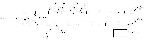
A page-width printhead for an ink printer. The printhead (102) comprises a
series of individual printhead elements (110, 112), each
having an array of ink ejection nozzles (7) formed therein. The series of
printhead elements extends substantially across the width of the
printhead, with respective end portions of adjacent elements (104, 106) being
located side by side in overlapping relationship. A dithering
unit (114) is provided for controlling the ejection of ink from the ink
ejection nozzles of the printhead elements and the dithering unit is
arranged, in use, to provide an overlap dithering matrix for a pair of the
respective end portions.


French Abstract

La présente invention concerne une tête d'impression de largeur de page pour une imprimante à encre. La tête d'impression (102) comprend une série d'éléments individuels de tête d'impression (110, 112), chacun présentant un réseau de buses d'éjection d'encre (7) constitué en son sein. La série d'éléments de tête d'impression s'étend sensiblement sur toute la largeur de la tête d'impression, avec des portions d'extrémité respectives d'éléments contigus (104, 106) étant situés côte à côte dans une relation de chevauchement. Une unité de juxtaposition (114) est prévue pour le contrôle de l'éjection d'encre à partir des buses d'éjection d'encre des éléments de tête d'impression et l'unité de juxtaposition est destinée, lors de son fonctionnement, à produire une matrice de juxtaposition de chevauchement pour une paire des portions d'extrémité particulière.

Claims

Note: Claims are shown in the official language in which they were submitted.


-4-
The Claims:
1 A page-width printhead (300) for an ink printer, the printhead comprising:
a series of individual printhead elements (302, 322), each having an array of
ink
ejection nozzles (305) formed therein, the series of printhead elements (302)
extending substantially across the width of the printhead (300), with
respective
end portions (314, 316) of adjacent elements (302, 322) being located side by
side
in overlapping relationship; and,
a dithering unit (304) being provided for controlling the ejection of ink from
the
ink ejection nozzles (305) of the printhead elements (302, 322); characterised
in
that,
during use, the dithering unit (304) arranges the ink ejection nozzles (305)
across
the length of the overlapping end portions (314, 316) of a pair of printhead
elements (302, 322) into a dither matrix, to provide an interpolation between
the
characteristics of the pair of printhead elements (302, 322).
2. A page-width printhead (300) as claimed in claim 1 wherein the ink ejection
nozzles (305) between the overlapping ends (314, 316) of the printhead
elements
(302, 322) are arranged into separate dither matrices by the dither unit
(304).
3. A page-width printhead (300) as claimed in claim 1 wherein the elements
(302,
322) are positioned obliquely with respect to one another to form a row of
lapped elements.
4. A page-width printhead (200) as claimed in claim 1 wherein the elements
(206,
208) are arranged in at least two parallel rows (202, 204), with the elements
in
each row being spaced apart from one another and with the end portions (214)
of
each element (206) in one row (202) overlapping the end portions (216) of
adjacent elements (208) in the adjacent row (204).

Description

Note: Descriptions are shown in the official language in which they were submitted.


CA 02370849 2001-10-18
WO 00/64680 PCT/AUOO/00340
-1-
PAGE-WIDTH PRINTHEAD
Field of the Invention
The present invention relates to a page-width printhead for an ink printer.
Background of the Invention
Page width printheads for ink printers typically are formed from a plurality
of
individual printhead elements (sometimes referred to as "chips"), with each
printhead
element having a plurality of ink ejection nozzles formed therein.
Because a plurality of individual printhead elements is employed in any one
printhead, achievement of a uniform print or print tone along the entire
length of the
printhead has so far been practically impossible. Non-uniformities or
variations occur
due to minor differences in the ink ejection nozzles in adjacent printhead
elements and
such variations may even occur when the elements originate from a single wafer
due to
inherent variations in process parameters that arise during the production of
elements on
a single wafer.
It is known that even slight variations in the print determining
characteristics of
adjacent elements in a page-width printheads will diminish the quality of the
resultant
print significantly, as the differences between adjacent areas of a print will
be
"amplified" in the visual perception of the print.
Summary of the Invention
In accordance with a first aspect of the present invention there is provided a
page-width printhead for an ink printer. The printhead comprises a series of
individual
printhead elements, each having an array of ink ejection nozzles formed
therein. The
series of printhead elements extends substantially across the width of the
printhead, with
respective end portions of adjacent elements being located side by side in
overlapping
relationship. A dithering unit is provided for controlling the ejection of ink
from ink
nozzles of the printhead elements and the dithering unit is arranged, in use,
to provide
an interpolation between the characteristics of a pair of printhead elements
across the
length of the overlapping end portions of the pair of printhead elements.
In one embodiment of the invention, the elements are positioned obliquely with
respect to one another to form a row of lapped elements.
In another embodiment, the elements are arranged in at least two parallel
rows,
with the elements in each row being spaced apart from one another and with the
end
portions of each element in one row overlapping the end portions of adjacent
elements
in the adjacent row.

CA 02370849 2001-10-18
WO 00/64680 PCT/AUOO/00340
.2-
In accordance with a second aspect of the present invention there is provided
a
method of controlling the ejection of ink from a page-width printhead as above
defined,
the method comprising the step of effecting an interpolation between the
characteristics
of a pair of printhead elements across the length of the overlapping end
portions of the
pair of printhead elements.
Description of the Drawings
Notwithstanding any other forms which may fall within the scope of the present
invention, preferred forms of the invention will now be described, by way of
example
only, with reference to the accompanying drawings, in which:
Figs. la and b are schematic illustrations of arrangements for positioning a
number of printhead elements in a single printhead row.
Fig. 2 illustrates a printhead embodying the present invention.
Fig. 3 illustrates a graph of dither probabilities for use with the printhead
of
Fig. 2.
Fig. 4 illustrates a second printhead embodying the present invention.
Fig. 5 illustrates a third printhead embodying the present invention.
Description of Preferred Embodiments
As shown in Fig. la, a CMOS processed wafer incorporating ink ejection
nozzles 100 is initially diced into printhead elements 1 and tested for
functionality of the
ink-jet nozzles. The testing can take various forms from full ink ejection
test to optical
examination of device operation. Once a determination is made of the
operational
characteristics of each ink ejection nozzle, the elements are joined together
into a longer
inkjet printhead row 3 as illustrated in Fig. lb. The printhead row 3 can
include eight
half-inch elements 1 and one quarter inch element 2 which are joined together.
Each
element 1 and 2 contains an array of a large number of the ink ejection
nozzles 100.
Next, as shown in Fig. 2, parallel printhead rows 5 and 6 are positioned side-
by-side so as to form a printhead 102. The two printhead rows 5 and 6 are
located with
respect to each other such that respective end portions 104 and 106 of
adjacent elements
of the two rows 5 and 6 are located side by side in overlapping relationship.
Further, the element boundaries 9 of the printhead row 5 are positioned so as
not to coincide with the element boundaries 108 of the printhead row 6.
In each of the printhead rows 5 and 6 it is likely that neighbouring elements
110 and 112 will have slightly different characteristics which, if each
printhead row was
utilised as an individual printhead, would result in unacceptable variations
in printing
across the width of a page. If the element 110 were to be taken from a first
wafer and

CA 02370849 2001-10-18
WO 00/64680 PCT/AUOO/00340
-3-
the element 112 taken from a second wafer, large variations across the element
boundaries would be likely.
In the printhead 102 however, a dithering unit 114 is provided to control the
ejection of ink from the nozzles 7 of the printhead 102. The dithering unit
114 is
arranged to provide an overlap dithering matrix for the printhead rows 5 and
6.
Various dithering schemes may be adopted. One probability interpolation 12
for use in the provision of the overlap dithering matrix is as illustrated in
Fig. 3.
In an alternative embodiment illustrated in Fig. 4, a printhead 200 comprises
two rows 202 and 204 of spaced apart printhead elements 206 and 208, the
elements
each being provided with an array of ink ejection nozzles 210. The printhead
further
comprises a dithering unit 212 which is arranged to provide integral dithering
matrices
for pairs of respective end portions 214 and 216 of adjacent elements 206 and
208 of the
rows 202 and 204. In regions 222 of the printhead 200 between the overlapping
end
portions, the dithering unit 210 is arranged to provide dithering matrices for
centre
portions 224 of the individual elements.
Fig. 5 shows an alternative embodiment for a printhead 300 which comprises a
row of individual printhead elements 302 positioned obliquely with respect to
one
another. The printhead 300 further comprises a dithering unit 304 for
cor}trolling the
ejection of ink from ink ejection nozzles 305 of the elements 302 of the
printhead 300.
The dithering unit 304 in this embodiment is arranged to provide integral
dithering
matrices for pairs of respective end portions 314 and 316 of adjacent elements
302 and
320. In regions 322 of the printhead 300 between the overlapping end portions,
the
dithering unit 304 is arranged to provide dithering matrices for centre
portions 324 of
the individual elements.
It will be appreciated by a person skilled in the art that numerous variations
and/or modifications may be made to the present invention as shown in the
specific
embodiments and the attached appendices without departing from the spirit or
scope of the
invention as broadly described. The present embodiments are, therefore, to be
considered
in all respects to be illustrative and not restrictive.

Representative Drawing
A single figure which represents the drawing illustrating the invention.
Administrative Status

2024-08-01:As part of the Next Generation Patents (NGP) transition, the Canadian Patents Database (CPD) now contains a more detailed Event History, which replicates the Event Log of our new back-office solution.

Please note that "Inactive:" events refers to events no longer in use in our new back-office solution.

For a clearer understanding of the status of the application/patent presented on this page, the site Disclaimer , as well as the definitions for Patent , Event History , Maintenance Fee  and Payment History  should be consulted.

Event History

Description Date
Inactive: COVID 19 - Reset Expiry Date of Patent to Original Date 2020-06-16
Inactive: COVID 19 - Deadline extended 2020-06-10
Inactive: COVID 19 - Deadline extended 2020-05-28
Inactive: COVID 19 - Deadline extended 2020-05-14
Inactive: COVID 19 - Deadline extended 2020-04-28
Inactive: Expired (new Act pat) 2020-04-20
Inactive: COVID 19 - Deadline extended 2020-03-29
Common Representative Appointed 2019-10-30
Letter Sent 2019-04-23
Letter Sent 2014-11-04
Letter Sent 2013-08-16
Inactive: Late MF processed 2012-08-30
Letter Sent 2012-04-20
Grant by Issuance 2008-09-30
Inactive: Cover page published 2008-09-29
Pre-grant 2008-07-08
Inactive: Final fee received 2008-07-08
Notice of Allowance is Issued 2008-02-11
Letter Sent 2008-02-11
Notice of Allowance is Issued 2008-02-11
Inactive: IPC removed 2008-02-06
Inactive: Approved for allowance (AFA) 2007-12-30
Amendment Received - Voluntary Amendment 2007-08-15
Inactive: S.30(2) Rules - Examiner requisition 2007-02-20
Inactive: Office letter 2006-07-18
Amendment Received - Voluntary Amendment 2006-07-17
Inactive: Corrective payment - s.78.6 Act 2006-06-30
Inactive: S.30(2) Rules - Examiner requisition 2006-03-27
Inactive: IPC from MCD 2006-03-12
Revocation of Agent Requirements Determined Compliant 2006-01-24
Inactive: Office letter 2006-01-24
Appointment of Agent Requirements Determined Compliant 2006-01-24
Revocation of Agent Request 2006-01-09
Appointment of Agent Request 2006-01-09
Inactive: IPRP received 2005-01-06
Letter Sent 2004-05-27
All Requirements for Examination Determined Compliant 2004-05-17
Request for Examination Requirements Determined Compliant 2004-05-17
Request for Examination Received 2004-05-17
Inactive: Entity size changed 2004-05-13
Change of Address Requirements Determined Compliant 2003-06-06
Revocation of Agent Request 2003-05-27
Appointment of Agent Request 2003-05-27
Inactive: Adhoc Request Documented 2002-12-10
Inactive: Withdraw application 2002-11-27
Letter Sent 2002-05-02
Inactive: Cover page published 2002-04-08
Inactive: First IPC assigned 2002-04-03
Letter Sent 2002-04-03
Inactive: Notice - National entry - No RFE 2002-04-03
Application Received - PCT 2002-03-06
Appointment of Agent Request 2002-01-04
Revocation of Agent Request 2002-01-04
Inactive: Correspondence - Formalities 2002-01-04
National Entry Requirements Determined Compliant 2001-10-18
Application Published (Open to Public Inspection) 2000-11-02

Abandonment History

There is no abandonment history.

Maintenance Fee

The last payment was received on 2008-02-22

Note : If the full payment has not been received on or before the date indicated, a further fee may be required which may be one of the following

  • the reinstatement fee;
  • the late payment fee; or
  • additional fee to reverse deemed expiry.

Patent fees are adjusted on the 1st of January every year. The amounts above are the current amounts if received by December 31 of the current year.
Please refer to the CIPO Patent Fees web page to see all current fee amounts.

Owners on Record

Note: Records showing the ownership history in alphabetical order.

Current Owners on Record
MEMJET TECHNOLOGY LIMITED
Past Owners on Record
KIA SILVERBROOK
Past Owners that do not appear in the "Owners on Record" listing will appear in other documentation within the application.
Documents

To view selected files, please enter reCAPTCHA code :


To view images, click a link in the Document Description column. To download the documents, select one or more checkboxes in the first column and then click the "Download Selected in PDF format (Zip Archive)" or the "Download Selected as Single PDF" button.

List of published and non-published patent-specific documents on the CPD .

If you have any difficulty accessing content, you can call the Client Service Centre at 1-866-997-1936 or send them an e-mail at CIPO Client Service Centre.


Document
Description 
Date
(yyyy-mm-dd) 
Number of pages   Size of Image (KB) 
Representative drawing 2002-04-04 1 3
Abstract 2001-10-17 1 49
Claims 2001-10-17 1 40
Drawings 2001-10-17 3 34
Description 2001-10-17 3 164
Claims 2007-08-14 1 41
Representative drawing 2008-09-15 1 3
Notice of National Entry 2002-04-02 1 195
Courtesy - Certificate of registration (related document(s)) 2002-04-02 1 113
Acknowledgement of Request for Examination 2004-05-26 1 176
Commissioner's Notice - Application Found Allowable 2008-02-10 1 164
Maintenance Fee Notice 2012-05-31 1 172
Late Payment Acknowledgement 2012-08-29 1 163
Maintenance Fee Notice 2019-06-03 1 181
PCT 2001-10-17 8 313
Correspondence 2002-01-03 1 34
Correspondence 2002-01-03 2 64
Correspondence 2002-05-01 1 20
Correspondence 2002-05-01 2 67
Correspondence 2003-05-26 1 35
Fees 2002-06-03 1 34
Fees 2004-04-14 1 41
PCT 2001-10-18 5 225
Fees 2005-04-11 1 34
Correspondence 2006-01-08 2 67
Correspondence 2006-01-23 1 13
Correspondence 2006-01-23 1 17
Correspondence 2006-07-17 1 16
Correspondence 2008-07-07 1 32