Note: Descriptions are shown in the official language in which they were submitted.
CA 02371066 2001-10-22
WO 00/65711 PCT/SE00/00761
OVERVOLTAGE PROTECTION
TECHNICAL FIELD
The invention relates to protection of differential input terminals of
amplifiers and
comparators and in particular to an amplifier of differential type having
protected input
terminals.
BACKGROUND OF THE INVENTION AND STATE OF THE ART
I many practically used circuits comprising an operational amplifier the
voltage
between the two input terminals of such an amplifier always is very close to
zero due to
the fact that feedback is used and that the gain of an operational amplifier
is very high. In
o contrast, a comparator is designed to provide an output signal representing
the voltage
between the two input terminals of the comparator and thus, in normal use in a
circuit
generally always some voltage exists between the input terminals of the
comparator.
However, the input voltage can due to the exterior circuits providing signals
to the input
terminals become too large what can destroy the comparator circuit. If the
feedback for
s an operational amplifier is not functioning properly such an amplifier can
also be
destroyed if the provided input voltage becomes too large. The reason of the
feedback
being non-operative can be that a large voltage is provided to the input at
the same time
as "slew-rate"-limiting is made on the output terminal of the operational
amplifier or that
the output terminal of the operational amplifier is connected to a too great
load.
2o Therefore, protection circuits are required both for operational amplifiers
and in
particular for comparators. The latter ones obviously have not, in
conventional circuits, a
mechanism limiting the voltage between the input terminals.
SUMMARY OF THE INVENTION
It is an object of the present invention to provide a simple and efficient
protection of
2s the input terminals of an amplifier of differential type.
The two input terminals of a transistor based amplifier of differential type
as
considered herein are thus in the conventional way the base terminals of the
input, active
amplifying transistors. The base-emitter junctions in the input transistors
are protected by
transistors connected as diodes in which the emitters and bases are connected
to each
ao other. The active pn junctions in the protection transistors are then the
junctions between
base and collector which normally have a greater breakthrough voltage in the
backward
direction then the pn junction between the base and the emitter. The
protection transistors
can advantageously be made in substantially the same way as the input
transistors and
have substantially the same electrical properties as them what makes it simple
to
35 introduce the protection in an electronic integrated circuit.
Thus, generally an amplifier of differential type is considered which
comprises two
amplifier transistors, the input terminals of the amplifier being directly
connected to the
bases of each of the amplifier transistors for receiving the input voltage,
the difference of
which is to be produced and/or amplified and is obtained as an output voltage
on an
CA 02371066 2001-10-22
WO 00/65711 PCT/SE00/00761
2
output terminal of the amplifier. The output voltage thus represents the
voltage between
the input terminals. Preferably, the output terminal is directly connected to
the collector
of one of the amplifier transistors.
For protection of the input terminals and in particular preventing that too
strong
currents will flow through the amplifier transistors, protective diodes are
connected
directly in series with the emitter of each of the first transistors. Each of
the protective
diodes is connected to have the same direction or polarity as the diode formed
by the pn
junction between the base and the emitter of the transistor to of which it is
connected.
Furthermore, the protective diodes are formed by protective transistors, the
emitter and
o the base of which are directly electrically connected to each other.
Generally then, not using the terms "emitter" and "collector", directly in
series with
that one of the pn junctions in each of the amplifier transistors which has
the lowest
breakthrough voltage in the backward direction a protective diode is connected
having the
same direction or polarity as the diode formed by the pn junction of the first
transistor
,s having the lowest breakthrough voltage. The protective diodes each comprise
a protective
transistor of the same polarity type as the amplifier transistors, which in a
differential
amplifier generally are substantially identical to other or at least have
substantially
identical electrical characteristics or properties. That one of the first and
second pn-
junctions in each of the protective transistors which has the lowest
breakthrough voltage
zo in the backward direction is short-circuited by a direct electrical
connection.
The amplifier transistors and the protective transistors can all be npn-
transistors of
substantially the same kind or all be pnp-transistors of substantially the
same kind.
BRIEF DESCRIPTION OF THE DRAWINGS
The invention will now be described as non limiting embodiments with reference
to
zs the accompanying drawings in which:
Fig. 1 is a circuit diagram of a simple transistor based differential
amplifier of a
previously known type,
Fig. 2 is a simplified circuit diagram of the amplifier of Fig. 1 in which
only some
essential components are drawn,
ao Fig. 3 is a schematic cross sectional view of a vertical npn-transistor.
Fig. 4 is a circuit diagram of a differential amplifier having protection of
the input
terminals of a previously known kind,
Fig. Sa is a picture which illustrates the equivalence between a transistor,
the base
and collector of which are directly electrically connected to each other, and
a diode,
a5 Fig. Sb is a picture illustrating the equivalence between a transistor, the
base and
emitter of which are directly electrically connected to each other, and a
diode,
Fig. 6a is a circuit diagram of an amplifier according to Fig. 2 having
protection of
the input terminals, the protection being obtained by as transistors connected
as diodes,
Fig. 6b is circuit diagram similar to that of Fig. 6a for transistors of other
CA 02371066 2001-10-22
WO 00/65711 PCT/SE00/00761
3
polarities, and
Fig. 7 is a circuit diagram of an amplifier according to Fig. 1 having the
same
protection of the input terminals as shown in Fig. 6a.
DESCRIPTION OF PREFERRED EMBODIMENTS
Hereinafter an amplifier circuit having some definite polarities of the
components
will be described. It is obvious to one skilled in the art that the amplifier
circuit can be
used with opposite polarities so that npn-transistors are replaced by pnp-
transistors and
vice versa, that the directions of a diodes are reversed, that positive
voltages become
negative and vice versa, that current directions are reversed, etc., provided
that
,o components are used which in other respects have corresponding or similar
electric
properties.
In Fig. 1 a circuit diagram of a common form of input stage is shown, the
input
stage being illustrated as a differential amplifier suited to be used in for
example
comparators or operational amplifiers. The two input terminals 1, 3 of the
circuit are
,5 constituted by the base terminals of two identical transistors T1 and T2 of
for example
npn-type as is shown in the figure. The emitters of the transistors Tl, T2 are
connected
to each other at an emitter node 5 and are there connected to the collector of
a third npn-
transistor T3 which is biassed by suitable voltages to work as a current
source and
thereby provides an emitter current to the input transistors T 1 and T2. The
emitter of the
zo third transistor can as shown in the figure be connected to some supply
voltage VEE, for
example a negative voltage a little offset from ground potential or the ground
potential
itself.
The collectors of the two first transistors T l and T2, the very amplifying
transistors
or input transistors, are connected to a supply voltage V~~, for example a
positive
2s constant voltage, in some suitable way, for example as is shown in the
figure through a
current mirror circuit. The current mirror circuit comprises two pnp-
transistors T4 and
T5, the bases of which are connected to each other and the emitters of which
are
connected to the supply voltage V~~. The pnp-transistor T4 for the first input
transistor
T1 further has its base and its collector connected to each other so that it
acts as a diode,
ao whereas these two transistors T4 and TS have their collectors coupled to
the collectors of
the respective input transistors T l and T2. The important fact associated
with the
connection of the input transistors T 1 and T2 to the drive voltage V~~ is
that the
transistors T4 and TS have an equivalent impedance and idling or no-load
voltage
(Thevenin-equivalent) so that the input transistors T1 and T2 work in their
active region,
35 i.e. they are not saturated, and thus the voltages from their collectors to
their bases
always are positive. Thereby the transistors T4 and TS in the current mirror
can be
replaced by resistors coupled between the collectors of the transistors and
the positive
supply voltage Vac.
A simplified embodiment of an input stage, shown partly schematically and
CA 02371066 2001-10-22
WO 00/65711 PCT/SE00/00761
4
comprising only the components essential in this context, are shown in Fig. 2.
Here the
transistor T3 is shown as a current generator I1, whereas the collectors of
the input
transistors T1 and T2 are only shown connected to generally denoted connection
nodes.
The output signal of the two circuits shown in Figs. 1 and 2 is in principle
the
s collector current through either one of the input transistors T 1, T2. A
voltage
representing this current can for example be extracted or retrieved at the
terminal 7 of the
collector electrode of the second input transistor T2.
When the voltage between the input terminals 1, 3 is small, the two input
transistors
T 1, T2 are active and current flows through their emitter terminals to the
common
o emitter node 5 . The current through these transistors are determined by the
current
source I1 or the transistor T3 respectively and is distributed among them so
that more
current will flow through the input transistor which has the highest voltage
on its input
terminal, i.e. on its base. When voltage between the input terminals becomes
sufficiently
large, sufficiently large being taken to mean that the voltage is equally to
some VT,
,s where VT is proportional to the absolute temperature and VT is about 26 mV
at ambient
temperature, the current through the input transistor, which has the lowest
potential on its
input terminal, can be neglected and the potential on the base or input
terminal of the
other input transistor is determined by the saturation current of this
transistor. The
voltage between the base and the emitter of this transistor is for saturation
approximately
zo given by VBE = VT~log(I1/IS), where I1 is the current generated by the
current generator
I1 and IS is the saturation current of the transistor.
Suppose now that the voltage on the input terminal 3 of the second input
transistor
T2 is maintained constant while the voltage on the second input terminal 1 of
the first
input transistor T1 is successively lowered. The voltage through the first
input transistor
zs T 1 will then be lowered until the voltage of the emitter node is
determined by the current
of the current generator I1 and the saturation current IS of the input
transistors. When the
voltage is further reduced, the pn junction between the base and emitter in
the first input
transistor T 1 will be forwardly biassed to a smaller and smaller extent in
order to then be
reverse-biassed. When the voltage finally becomes sufficiently negative,
current will
ao again flow through the emitter of the first input transistor T 1 but now in
an opposite
direction depending on the breakthrough voltage of said pn junction being
exceeded. All
of this current then passes out through the first input terminal 1, i.e. the
base of the first
input transistor T1. The current is then no longer determined by the current
source Il but
by the driving capability of the exterior voltage sources and by the
resistances of the two
as input transistors T1 and T2. In any case, the current can destroy the two
input transistors
T 1, T2 but perhaps primarily the first input transistor T 1 in which the
developed power
becomes greatest. The voltage which an npn-transistor can allow between its
emitter and
base before the reverse-biassed pn junction starts to conduct current varies
between
different manufacturing processes and different component layouts. For signal
processing
CA 02371066 2001-10-22
WO 00/65711 PCT/SE00/00761
transistors usually this current is greater than about 6 V and smaller than
about 10 V .
Generally, a bipolar transistor consists of three regions which are located at
each
other in a row and which often comprise layers located on top of each other,
made of
semiconductor material having alternating polarities so that a middle region
and two
5 exterior regions exist. A bipolar transistor can then be npn-type or pnp-
type. A
connection to exterior circuits is provided from each region which can also be
called an
electrode. The middle region is called the base and the two exterior regions
comprise the
collector and the emitter respectively. If voltages are applied to the
terminals of an npn-
transistor so that V~ > Vb > Ve for an npn-transistor, and to a pnp-
transistor, so that V~
,o < Vb < Ve, where V~, Vb, Ve are the potentials on the collector, base and
emitter
respectively of the transistors, and if a not too large current is supplied to
the base which
should also be positive for an npn-transistor and negative for a pnp-
transistor, the current
through the collector of the transistor is controlled by the supplied base
current. Roughly,
the collector current can be proportional to the base current. The constant of
s proportionality is called BF, "forward current gain" , also denoted by /3.
An arbitrary one of the two exterior regions of bipolar transistor could then
be
called the emitter whereas the other region then is the collector of the
transistor. Usually
however, the collector and emitter are defined so that the constant ~3 of
proportionality
becomes as large as possible. For the same polarities of the applied voltages,
if the
Zo transistor is turned around so that the collector will be located where the
emitter
previously was located, it is possible to measure a corresponding constant of
proportionality or current gain factor BR, "reverse current gain" . Usually BF
is much
larger than BR. This fact depends on several optimizations of the layout or
structure of
the transistors, these optimizations considering among other things that it is
desirable to
25 have a BF which is as large as possible, i.e. one of the gain factors
should be given the
highest possible value. The value of BR has less importance. Usual values are
BF = 50 -
100 and BR = 0.5 - 10. It is important to observe that an obvious condition of
using a
transistor in an amplifier circuit is that it has a current gain factor larger
than one.
The most common embodiment of an npn-transistor in integrated circuits is a
ao vertical transistor, as illustrated by the cross-sectional schematic view
of Fig. 3. In some
outer material 11, having a low doping of the same type as the base, layers
are provided
which form the parts or regions of the transistor. The collector 13 is the
lowermost layer
having a doping opposite that of the outer material. Centrally in this
lowermost layer
another layer 15 is located forming the base and centrally in the base region
a further
35 layer 17 is located forming the emitter, so that in the centre of structure
a layer sequence
is obtained comprising, from the bottom and upwards, collector, base and
emitter. The
different regions extend at the exterior edges up to the surface of the
structure for
exterior electrical connection. Such a transistor is made so that the doping
levels are
decreasing in the order emitter-base-collector, i.e. the emitter region has a
higher doping
CA 02371066 2001-10-22
WO 00/65711 PCT/SE00/00761
6
than the base region and the base region has a higher doping than the
collector region.
Furthermore, the base layer 15 is very thin at the centre of the structure and
the collector
layer is relatively thick. This contributes to the desired properties
comprising a high
current gain factor BF and good high frequency properties. The same properties
also
a result in that the breakthrough voltage BV~b, when the collector-base
junction is reverse-
biassed, becomes significantly higher than the breakthrough voltage BVeb, when
the
emitter-base junction is reverse-biassed. In manufacturing processes which
have been
optimized therefor often the breakthrough voltage BV~b between collector and
base is of
the magnitude of order 50 - 120 V, which is to be compared to the breakthrough
voltage
,o BVeb of 6 - 12 V for the emitter-base junction. Such manufacturing
processes are used in
applications which require that the circuits can stand high voltages, for
example in
circuits for audio amplifies, voltage converters, electronic circuits for
vehicles, etc.
A previously known way of protecting the input stage as described above
comprises
connecting resistors Rl, R2 at the input terminals in series with the base
terminals of the
s input transistors T 1, T2 according to Fig. 3 . Thereby the base currents
are limited.
Furthermore, diodes D 1, D2 can be connected between the emitters and bases of
these
transistors so that these diodes conduct in a direction opposite the base-
emitter-diode in
each transistor. Thus, when the backward voltage between emitter and base of
one of the
transistors T 1, T2 exceeds the forward voltage for the corresponding exterior
diode D 1,
zo D2 connected antiparallel, the forward voltage being about 0.6 to 1 V, the
current will be
conducted through the exterior diode instead of being conducted through the
respective
transistor. An advantage of such a circuit solution comprising protective
components is
that the transconductance of the input stage in normal operation is not
effected by the
added protective components. It is well known that in manufacturing integrated
circuits,
2s when in the manufacturing process only transistors are available, diodes
are obtained by
connecting the base and collector of a transistor to each other, see Fig. Sa.
Due to the
two pn junctions existing in a transistor obviously also a component having a
diode
function is obtained in the case where the base and emitter of the transistor
are connected
to each other, see Fig. Sb. However, such a diode component is seldom used,
since it
ao gets worse properties for most applications compared to a diode obtained by
connecting
the collector and the base of a transistor to each other.
However it appears, that by using a bipolar transistor in an unconventional
way it is
possible to obtain a protection of the input terminals of differential
amplifiers as
described above. As has been mentioned above, in a transistor in most cases a
high
35 current gain is desired. In the application described hereinafter this is
not necessary.
In Fig. 6a a principle circuit diagram of a differential amplifier is shown
which is
constructed substantially as the amplifier shown in Figs. 1 and 2 and which
has protection
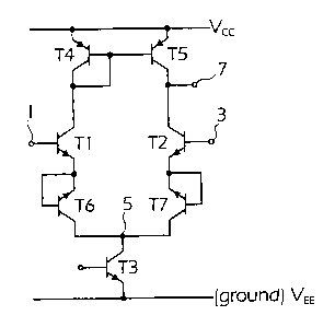
of the input terminals. A more complete circuit diagram is shown in Fig. 7.
This circuit
solution has two npn-transistors T6, T7 connected between the emitters of the
input
CA 02371066 2001-10-22
WO 00/65711 PCT/SE00/00761
7
transistors T1, T2 and the common emitter node 5. These transistors have their
base
terminals connected to the respective emitter terminals so that only the base-
collector
diode is used. They are connected so that the emitter in a normal operation of
the
amplifier has a higher potential then the collector-base, e.g. the base-
collector-diode is
forwardly biassed.
If, in the same way as has been discussed above, the input voltage on the base
3 of
the second input transistor T2 is maintained constant while the voltage on the
other input
terminal 1, i. e. the voltage on the base of the first input transistor T 1,
is gradually
reduced, again firstly the current through the first transistor is lowered
down to a zero.
,o After some further reduction of the input voltage current will flow
"backwards" in the
direction from the emitter to the base in the first transistor T 1 but now it
will start to
flow until the voltage between the node 5 and the input terminal 1 exceeds the
sum of the
breakthrough voltage BVeb between the emitter and base of 'the transistor T1
and the
breakthrough voltage BV~e between the collector and emitter of the protective
transistor
,5 T6. The breakthrough voltage BV~e between the collector and the emitter in
a transistor
is considerably, i.e. many times, larger than the breakthrough voltage BVeb
between the
emitter and base in the same transistor and is further of the same magnitude
of order as
the breakthrough voltage BV~b between the collector and base, as has been
defined
above. In the protected circuit solution according to Fig. 4 the current surge
in the input
Zo transistor T 1 occurs already when the voltage between the node 5 and the
input terminal
1 exceeds the breakthrough voltage BVeb between the emitter and the base of
the input
transistor.
In Fig. 6b a principle circuit diagram of a differential amplifier similar to
that of
Fig. 6a in which instead npn-transistors are used both as amplifying or active
elements
z5 and as protective elements. This circuit operates in basically the same way
as the circuit
illustrated in Figs. 6a and 7.
The advantage of the circuit solution according to Figs. 6a and 7 or Fig. 6b
is thus
that the circuit can stand voltages which are many times higher compared to
the case
having no protective components. Compared to the known circuit solution
according to
ao Fig. 4 two advantages exist. In the known solution a current passes through
the protective
components R1, R2, D1, D2, when the protection becomes operative. Such a non-
controlled current can among other things result in overheating. This is not
the case for
the solution according to Figs. 6a and 7. Furthermore, resistors are often not
suited to be
integrated in monolithic integrated circuits, either due to the fact that the
manufacturing
35 process in itself is not suited for manufacturing resistors or due to the
fact that they
occupy a too large area on a circuit plate. In integrated circuits resistors
are longer the
larger resistance they have. Since the widths of the resistors are not allowed
to be smaller
than a definite smallest measure determined by mask production, optical
resolution, etc.
and the resistance then is determined by the ratio of the length and the
width, resistors
CA 02371066 2001-10-22
WO 00/65711 PCT/SE00/00761
8
having high resistance values obtain a great length and thereby large areas.
In the
protective circuit according to Fig. 4 the power generation in the resistors
R1, R2 can
become significant in the case where the other components in circuits, not
shown, feeding
the input terminals of the amplifier circuit allow it.
s The transistors T6, T7 connected as diodes in the circuit according to Figs.
6a, 6b
and 7 influence the transconductance of the differential amplifier. This can
be an
advantage or disadvantage. Thus, in some previously known circuits resistors
can be used
connected at the positions of the protective transistors T6, T7 to lower the
transconductance.