Note: Descriptions are shown in the official language in which they were submitted.
CA 02371140 2001-10-31
WO 00/69192 PCTNS00/12474
METHOD OF PROFILING DISPARATE COMMUNICATIONS
AND SIGNAL PROCESSING STANDARDS AND SERVICES
CROSS REFERENCE TO RELATED APPLICATION
This application claims priority from the Provisional Application entitled
"Apparatus and Method for Profiling Disparate Communications and Signal
Processing Standards and Services", U.S. Serial No. 60/133,130, filed May 7,
1999.
BRIEF DESCRIPTION OF THE INVENTION
This invention relates generally to the design of multi-function digital
devices.
More particularly, this invention relates to a technique for profiling
disparate
communications and signal processing standards and services to facilitate the
development of an application-specific processor.
BACKGROUND OF THE INVENTION
Signal processing protocols and standards have proliferated with advances in
wireless communications devices and services. Current communications protocols
include Frequency Division Multiplexing (FDM), Time Division Multiple Access
(TDMA) and Code Division Multiple Access (CDMA). The United States, Europe,
Japan and Korea have all developed their own standards for each communications
protocol. TDMA standards include Interim Standard-136 (IS-136), Global System
for
Mobile (GSM), and General Packet Radio Service (GPRS). CDMA standards include
CA 02371140 2001-10-31
WO 00/69192 PCT/US00/12474
Global Positioning System (GPS), Interim Standard-95 (IS-95) and Wide Band
CDMA
(WCDMA). Wireless communications services include paging, voice and data
applications.
Until recently wireless communications devices supported a single
communications standard. In theory, a wireless communications device can be
designed using a general purpose Digital Signal Processor (DSP) that would be
programmed to realize a set of functional blocks specifying the minimum
performance
requirements for the application. To achieve these minimum performance
requirements, system designers design algorithms (sequences of arithmetic,
trigonometric, logic, control, memory access, indexing operations, and the
like) to
encode, transmit, and decode signals. These algorithms are typically specified
in
software. The set of algorithms which achieve the target performance-
specification is
collectively referred to as the executable specification. This executable
specification
can then be compiled and run on the DSP, typically via the use of a compiler.
Despite
the increasing computational power and speeds of general purpose DSPs and
decreasing memory cost and size, designers have not been able to satisfy cost,
power
and speed requirements simply by programming a general purpose DSP with the
executable specification for a standard-specific application.
Additional dedicated high-speed processing is required, a need which has
traditionally been met using an application-specific processor. As used
herein, an
application-specific processor is a processor that excels in the efficient
execution
(power, area, flexibility) of a set of algorithms tailored to the application.
An
application-specific processor fares extremely poorly for algorithms outside
the
intended application space. In other words, the improved speed and power
efficiency
of application-specific-processors comes at the cost of function flexibility.
Demand is now growing for wireless communications devices that support
multiple applications and varying grades of services over multiple standards.
Today's
solution to this problem is to essentially connect multiple application-
specific
processors together to obtain mufti-standard operation, thereby adding cost in
terms of
design resources, design time, and silicon area. Figure 1 illustrates, in
block diagram
form, a wireless communications device designed with this approach. Figure 1
includes a micro-controller core 20 and a DSP 22 having access to a memory 24.
The
2
CA 02371140 2001-10-31
WO 00/69192 PCT/US00/12474
wireless communications device also includes a set of application-specific
fixed
function circuits 26A-26D, including an AMPS circuit 26A, a CDMA circuit 26B,
an
IS-136 circuit 26C, and a GSM circuit 26D.
In view of the foregoing, it would be highly desirable to eliminate
application-
specific communications and signal processors by providing a technique for
profiling
disparate communications and signal processing standards to facilitate the
implementation of a single processor to support the disparate communications
and
signal processing standards in a cost, area and power efficient fashion.
SUMMARY OF THE INVENTION
The method of the present invention profiles disparate communications and
signal processing standards to define a programmable processor that may be
programmed to execute any of the disparate communications and signal
processing
standards. The method includes the steps of selecting a set of communications
and
signal processing standards for analysis and identifying functions common to
the
selected set of communications and signal processing standards. Thereafter,
the
common functions are ranked according to computational intensity. Using this
ranking, a set of high computational intensity functions are selected for
implementation as kernels, the set of kernels forming a programmable processor
with
which any one of the set of communications and signal processing standards can
be
implemented.
The invention enables the identification of optimum datapaths and control
state-machines for use in the design of application-specific processors. The
methodology can be used to identify functions that are poorly executed by
existing
microprocessors and digital signal processors. The technique can also define
new
datapaths and state-machines required to efficiently implement functions. The
methodology of the invention offers a systematic way to analyze functions
across
many applications or standards, thereby reducing the time to define a
processor
architecture and increasing the amount of design reuse possible in the design
of new
processors for digital signal processing of mufti-standard applications.
CA 02371140 2001-10-31
WO 00/69192 PCT/US00/12474
BRIEF DESCRIPTION OF THE DRAWINGS
For a better understanding of the invention, reference should be made to the
following detailed description taken in conjunction with the accompanying
drawings,
in which:
FIGURE 1 illustrates a prior art communications and signal processing system
utilizing a set of application-specific processors.
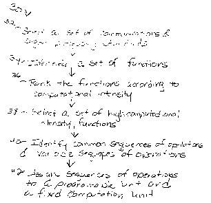
FIGURE 2 illustrates the steps of profiling communications and signal
processing functions across multiple standards in accordance with an
embodiment of
the invention.
FIGURE 3 illustrates the canonical function blocks of a receiver.
FIGURE 4 illustrates a set of sub-functions for implementing a Parameter
Estimator.
FIGURE 5 illustrates a table ranking sub-functions according to computational
intensity.
FIGURE 6 illustrates a Kernel for implementing a function.
FIGURE 7A illustrates a first portion of a method of identifying the
components of an add-compare-select loop of a Viterbi algorithm.
FIGURE 7B illustrates a second portion of a method of identifying the
components of an add-compare-select loop of a Viterbi algorithm.
FIGURE 7C illustrates a third portion of a method of identifying the
components of an add-compare-select loop of a Viterbi algorithm.
FIGURE 8 illustrates a method of identifying the critical sequence of
operations for a Finite Impulse Response Filter (FIR).
FIGURE 9 illustrates the process of profiling canonical functions.
FIGURE 10 illustrates a programmable multi-standard application-specific
Processor.
FIGURE 11 illustrates an example of necessary programmable interconnections
between Kernels for a given application.
Like reference numerals refer to corresponding parts throughout the drawings.
4
CA 02371140 2001-10-31
WO 00/69192 PCT/US00/12474
DETAILED DESCRIPTION OF THE INVENTION
Figure 2 illustrates the steps 30 of the method of the present invention for
profiling
and analyzing functions across many signal processing applications to design a
processor
that can be programmed to efficiently execute the algorithms associated with
any of the
profiled signal processing standards or applications. The process of Figure 2
will reduce
the time to define a processor architecture and increases the amount of design
reuse
possible in the design of new processors for digital signal processing of
mufti-standard
applications. Briefly described, the method of the present invention begins
with the
selection of a set of communications and signal processing standards and
services for
analysis. Next, functions common to the selected set of communications and
signal
processing standards are identified. Thereafter, the common functions are
ranked
according to computational intensity and a set of high computational intensity
functions
are selected for implementation as programmable kernels, these kernels forming
a
programmable mufti-standard processor.
First, during step 32 a set of communications and signal processing standards
are
selected for analysis from the set of possible standards. Any arbitrary set of
standards
may be selected in compliance with the present invention; however, it is
likely that the
standards selected will be influenced by the target market for the
programmable processor
being designed. For example, the target market might be manufacturers of
wireless
mobile devices intended for sale in Japan.
A. Identifying Common Canonical Functions
Still referring to Figure 2, after a set of communications and signal
processing
standards have been selected, a set of common functional blocks are identified
for the
selected application during step 34. As an example, Figure 3 illustrates the
functional
blocks when the selected application is Baseband Processor 51 of a receiver.
The
functional blocks to be implemented are Digital Front-End Processor 52,
Detector/Demodulator 54, Symbol Decoder 56, Source Decoder 58, and Parameter
Estimator 60. For each of the functional blocks of Baseband Processor 51, each
of the
selected communications and signal processing standards will specify a number
of sub-
functions. For example, consider Figure 4, which illustrates in tabular form
the set of sub-
functions to implement Parameter Estimator 60 for a number of standards. Many
S
CA 02371140 2001-10-31
WO 00169192 PCT/US00/12474
Parameter Estimation sub-functions are common to multiple standards. For
example, IS-
136, GSM, GPRS, EDGE, IS-95B, IS-2000 and WCDMA-FDD all use the Windowed
Average Energy Estimator.
B. Ranking Functions
Figure 2 illustrates that during step 36 the functional blocks are ranked to
identify
functions ill-suited to realization via programming of a general purpose DSP.
Stated
another way, the functions are ranked to identify those suited to
implementation via an
application-specific mufti-standard processor. This is a mufti-step process
that begins
with generating the executable specification for each function across the
selected
communications and signal processing standards. Preferably, the executable
specification
is coded using either the C or C++ language. The executable specification for
each
standard may then be ranked using a number of metrics. One useful metric is
the
computational intensity of each function. The computational intensity of each
function
may be determined using dynamic profiling of each executable specification to
quantify
the associated number of millions-of operations-per-second (MOPS). This may be
done
via simulations and automated test benches. The results may be presented in a
table
demonstrating which functions have the highest MOPS. This characterization can
be
made with a generic processor or with respect to a particular digital signal
processor or
microprocessor. If a characterization is made with respect to a specific
processor, the
executable specification must run on that processor for profiling purposes.
The table that
results from this exercise shows functions for which the instruction set
architecture,
datapath, or memory bandwidth of the native processor is not necessarily well-
suited.
Figure 5 illustrates a portion of such a table, which includes MOPS for a
single
standard and a subset of sub-functions of Baseband Processor 51 (see Fig. 3).
The
computational intensity of each sub-function is indicated for a subset of the
channels
supported by Baseband Processor 51. Figure 5 indicates that the Receive (Rx)
Filter is
the most computationally intensive of the listed sub-functions and, as such,
is the best
suited for implementation in a programmable application-specific processor.
Figure 5
also indicates that the Complex Despreader is computationally intensive and
well-suited
to implementation is a programmable application-specific processor. Other sub-
functions
6
CA 02371140 2001-10-31
WO 00/69192 PCT/US00/12474
likely to be computationally intensive, but which are not illustrated in
Figure 5, are RAKE
receivers, Turbo Coders, Interference Cancellers, Multi-user Detectors and
Searchers.
Other metrics that may be used to rank the functions across the selected set
of
communications and signal processing standards include power consumption and
silicon
area. Determining the power consumption of each function requires identifying
the
amount of time spent by the function on each of a set of operation types. The
set of
operation types includes move-and-transfer, loop-and-control, trigonometric
and
arithmetic. Each type of operation consumes some number of mW per operation.
Thus,
given the number of operations of each type the total power consumption of
each function
can be determined across the selected set of communications and signal
processing
standards. Such an analysis is likely to reveal that RAKE receivers tend to
consume a
great deal of power as compared to other sub-functions. The silicon area
required to store
the executable code can be estimated for each function across the selected set
of
communications and signal processing standards by counting the number and
types of
operations required for each of the executable specifications, and then using
a cost table
showing the cost in silicon areas for each operator. Once again, RAKE
receivers are likely
to require many more gates to store their executable code than are other sub-
Functions.
After the functions have been ranked using the selected set of metrics, during
step
38 (see Fig. 2) a set of highly ranked functions are selected for
implementation and further
analysis.
C. Analysis and Assignment of Highly Ranked Functions
Referring again to Figure 2, during step 40 the selected set of functions are
analyzed for similarity across multiple standards to identify the computation
kernels that
are common across all instances of a function. (As used herein, kernel means a
sequence
of operations that may be represented by a control-dataflow graph and may be
implemented in either software or hardware. Figure 6 illustrates, in block
diagram form,
Kernel 65, which includes three modules: a Sequencer 66, a local Memory 67,
and a
parameterizable, configurable Arithmetic Logic Unit 68. ) In other words,
during step 40
a function-centric, rather than an application-centric, approach is taken to
profile functions.
The profiling of the functions begins with an executable specification of each
"standard-specific" version of the function and a simulation to optimize all
signal and
7
CA 02371140 2001-10-31
WO 00/69192 PCT/US00/12474
variable word-widths. The profiling of functions includes identification of
critical
sequences of operations. Sequences of operations may involve move-and-
transfer, loop-
and-control, trigonometric or arithmetic operations. As used herein, critical
sequences of
operations, or components, are those sequences of operations whose timely
completion is
necessary to performing a canonical function in a fixed period of time. As an
example,
Figures 7A-7C illustrate a method of identifying the components of an add-
compare-select
loop of a machine implemented Viterbi algorithm. A machine implemented Viterbi
algorithm is a dynamic-programming algorithm employed in digital
communications to
find the most likely sequence of transmitted symbols in a digital transmission
system.
Figure 7A describes the first two steps of a computer implemented Viterbi
algorithm.
Figure 7B illustrates the third step of a machine implemented Viterbi
algorithm, the add-
compare recursion, which includes a compute stage and a survivor storage
stage. Figure
7C illustrates the data flow and control flow of the add-compare-select
recursion of the
computer implemented Viterbi algorithm. Figure 7C shows the loop with the
sequence
of operations that are used during the recursion and the relationship between
the sequence
of operations for one iteration of the computer implemented Viterbi algorithm.
As yet another example of a method of identifying components of a canonical
function, Figure 8 illustrates a machine implemented method of identifying the
critical
sequence of operations for a Finite Impulse Response Filter (FIR). The
illustrated
equation describes mathematically the convolution of an input sequence x(n)
with a set of
filter coefficients a(n). The structure illustrated beneath the equation in
Figure 8 illustrates
the most common subset of data flow and control flow operations in realization
of the FIR.
Highlighting in Figure 8 illustrates the all the computation required for a
single stage of
the FIR.
After profiling the functions, the canonical functions are analyzed across
multiple
standards to identify the components that are common across all instances of
the function,
and those components that are variable. The process of profiling canonical
functions is
more fully appreciated with reference to Figure 9. At the bottom of Figure 9 a
set of
independent standards for wireless applications are listed, including GPS, IS-
95 CDMA,
W-CDMA, IS-136 TDMA, and GSM. A function profile for a particular application,
in
this case Baseband Processor 51, is listed on the left of Figure 9. The
canonical functions
8
CA 02371140 2001-10-31
WO 00/69192 PCT/US00/12474
of Baseband Processor 51 include an MPSK frequency estimator, a convolutional
decoder,
a rake receiver, and an MLSE equalization unit.
Figure 9 represents as rectangles the Functional Component Collections 70a-g,
72a-d, 74a-d and 76a-b which make up each canonical function. Each rectangular
Functional Component Collection is divided into a multiplicity of squares,
with each
square representing a single Component 71 &73. While Functional Component
Collections 70, 72, 74 & 76 are illustrated as including six Components 71
&73, the
number of Components 71 &73 per Functional Component Collection varies with
each
canonical function. For each Functional Component Collection 70, 72, 74 & 76
an
arbitrary number of Components 71 &73 are included for purposes of
illustration. In
Figure 9 Components 73 common to all Functional Component Collections for a
canonical
function are white, while those Components 71 which differ are black. An
arbitrary number
of variable and common Components are illustrated. Analysis of the Functional
Component Collections 70a-70d for a MPSK Frequency Estimator reveals three
Components 73 common to all CDMA standards and three Components 71 that vary
with
CDMA standard. This indicates a single set of Kernels may be designed to
support all
CDMA standards, provided that the set of Kernels is partially programmable to
permit
implementation of variable Components 71. In Similarly, analysis of the
Functional
Component Collections 70e-70g reveals three Components 73 common to all TDMA
standards and three Components 71 that vary with TDMA standard. This permits a
single
set of Kernels to be designed to support all TDMA standards profiled, provided
that the
set of Kernels is partially programmable. (Partial programmability is
necessary to allow
implementation of the variable Components 73.) Indeed, profiling reveals that
a single set
of partially programmable Kernels 78 may be designed to support all CDMA and
TDMA
Functional Component Collections 70a-g. Analysis of the Functional Component
Collections associated with the other canonical functions gives rise to
similar conclusions.
In other words, a single set of partially programmable Kernels 82 may be
designed to
support all Functional Component Collections 72a-72d associated with the
Convolutional
Decoder function; a single set of partially programmable Kernels 84 may be
designed to
supportthe Functional Component Collections 74a-74d associated with the Rake
Receiver
Function; and a single set of partially programmable Kernels 86 may be
designed to
9
CA 02371140 2001-10-31
WO 00/69192 PCT/US00/12474
support the Functional Component Collections 76a-76b associated with the MLSE
Equalization function.
For those functions with extensive overlap, during step 42 (See Fig.2) a
partially
programmable set of kernels, each with designed with a fixed computation unit
and a
programmable unit. As discussed with respect to Figure 6, a Kernel 65 includes
three
modules 66, 67, 68, which form a computational unit. Preferably, Sequencer 66
and ALU
68 are partially programmable. Thus, those programmable parts of Sequencer 66
and ALU
form the programmable computation unit, while Memory 67 and the fixed parts of
Sequencer 66 and ALU 68 form the fixed computation unit. By programming a
Kernel's
programmable unit all of its Components 71 and 73may be realized.
Referring again to Figure 9, sets of partially programmable Kernels 78, 82, 84
and
86 enable creation of a mufti-standard, protocol-specific Engines 90 and 94.
Engine 90
is a standard-independent, CDMA-specific processor that includes a set of
partially
programmable set of Kernels for each canonical function of an application.
Thus, Engine
90 may include, as an example, partially programable set of Kernels 78, 82, 84
and 86.
Similarly, Engine 92 is a standard-independent, TDMA-specific processor that
includes
a set of partially programmable set of Kernels for each canonical function of
an
application. Additionally, given a partially programmable set of Kernels for
each
canonical function a mufti-standard, protocol independent Engine 94 may be
designed.
Figure 10 illustrates, in block diagram form, a programmable, mufti-standard,
application-specific Processor 100. Processor 100 includes Program Control
Unit 102, a
Kernel Bank 104, and Reconfigurable Data Router 106. Program Control Unit 102
controls the programming of Kernel Bank 104 and Reconfigurable Data Router 106
so that
Processor 100 may be configured to support any one of a set of supported
standards.
Program Control Unit 102 includes Memory 110, which stores executive code for
programming Controller 112 and Bus Manager 114. Controller 112 controls the
programming of the programmable units within each Kernel of Kernel Bank 104,
while
Bus Manager 144 controls the configuration of Reconfigurable Data Router 106.
Kernel
Bank 104 includes a multiplicity of Kernels, one for each canonical function
of the
application. Reconfigurable Data Router 106 routes data between Kernels as
necessary
to implement the application according to a particular standard.
Reconfigurable Data
Router 106 need not be completely programmable. Figure 11 is an example of the
CA 02371140 2001-10-31
WO 00/69192 PCT/US00/12474
interconnections between Kernels that must be programmable for a given
application. The
Kernels of the application are listed both at the top and to the left of
Figure 11.
Interconnections that must be supported for the application are indicated by
an x. For each
Kernel there are relatively few interconnections that must be supported. For
example, the
Turbo Decoder Core kernel need only be capable of connecting to the
Convolutional
Decoder Core Unit kernel and the Memory Management Unit kernel.
Those skilled in the art will appreciate that the invention provides a
systematic
method for dealing with designing processors for multiple standards, multiple
functions,
and multiple parameters. In addition, the technique of the invention reduces
processor
design cycle time via function profiling and definition of datapath and
control state-
machine engines that can be reused across many processors.
The foregoing description, for purposes of explanation, used specific
nomenclature
to provide a thorough understanding of the invention. However, it will be
apparent to one
skilled in the art that the specific details are not required in order to
practice the invention.
In other instances, well known circuits and devices are shown in block diagram
form in
order to avoid unnecessary distraction from the underlying invention. Thus,
the foregoing
descriptions of specific embodiments of the present invention are presented
for purposes
of illustration and description. They are not intended to be exhaustive or to
limit the
invention to the precise forms disclosed, obviously many modifications and
variations are
possible in view of the above teachings. The embodiments were chosen and
described in
order to best explain the principles of the invention and its practical
applications, to
thereby enable others skilled in the art to best utilize the invention and
various
embodiments with various modifications as are suited to the particular use
contemplated.
It is intended that the scope of the invention be defined by the following
claims and their
equivalents.
11