Note: Descriptions are shown in the official language in which they were submitted.
CA 02371630 2002-02-13
SEMICONDUCTOR CHIP HAVING AN ARRAYED WAVEGUIDE
GRATING AND METHOD OF MANUFACTURING THE
SEMICONDUCTOR CHIP AND MODULE CONTAINING THE
SEMICONDUCTOR CHIP
BACKGROUND OF THE INVENTION
1. Field of the Invention
[0001] The present invention relates to a semiconductor chip obtained by
cutting, from a wafer, an element occupying a non-rectangular area. The
present
invention also relates to a module containing an element occupying a non-
rectangular area. For example, the present invention relates to a chip and a
manufacturing method thereof such as an arrayed waveguide grating chip, a
manufacturing method thereof, and manufacturing a module containing an
arrayed waveguide grating chip.
2. Description of the Related Art
[0002] As the volume of data to be transmitted increases, there is a
corresponding demand for a larger transmission capacity in an optical fiber
communications system. In addition, optical wavelength filtering is becoming
increasingly important as an optical multiplexing/demultiplexing device for
multiplexing and/or demultiplexing different wavelengths in Dense Wavelength
Division Multiplexing (DWDM) systems. There are various types of optical
wavelength filters. Among these, an arrayed waveguide grating has the desired
wavelength characteristics such that a high extinction ratio is obtained in a
narrow band region, and also features a filter device having multiple inputs
and
outputs. An arrayed waveguide grating is capable of multiplexing or
CA 02371630 2002-02-13
demultiplexing signals, allowing a wavelength multiplexing/demultiplexing
device can be easily constructed. Further, when the arrayed waveguide grating
is constructed with quartz waveguides, the arrayed waveguide grating couples
well with optical fibers and operates at small insertion loss, i.e., on the
order of
several dB (decibels). Due to these advantages, the arrayed waveguide grating
is gaining recognition as a particularly important device among the optical
wavelength filters.
[0003) FIG. 1 shows an overall structure of a related arrayed waveguide
grating. An arrayed waveguide grating comprises one or plural input waveguides
12 formed on a substrate 11, a plurality of output waveguides 13, a channel
waveguide array 14 wherein the respective arrayed waveguides are curved in a
certain direction, each waveguide having a different curvatures. The arrayed
waveguide grating further comprises an input side slab waveguide 15 for
connecting the input waveguides 12 with the channel waveguide array 14, and an
output side slab waveguide 16 for connecting the channel waveguide array 14
with the output waveguides 13. Multiplexed optical signals entering from the
input waveguides 12 have their propagation paths expanded at the input side
slab
waveguide 15 before entering the channel waveguide array 14. W the charnel
waveguide array 14, the individual arrayed waveguides comprising the channel
waveguide array 14 have mutually different optical path lengths. The
individual
arrayed waveguides are configured to progressively become either longer or
shorter. Therefore, light propagating through the individual arrayed
waveguides
of the charnel waveguide array 14 are imparted with predetermined phase
-2-
CA 02371630 2002-02-13
differences before reaching the output side slab waveguide 16. As a result,
light
is focused (condensed) at mutually different positions on the interface of the
output side slab waveguide 16 and the output waveguides 13 depending on
wavelength. Since the output waveguides 13 are arranged at positions
corresponding to different wavelengths, any given wavelength component can be
taken from one of the output waveguides 13. Refernng to FIG. 2, arrayed
waveguide gratings 10 are commonly formed on a wafer comprising a silicon
base or a quartz base. The wafer has a substantially disk-like shape, on which
a
plurality of the arrayed waveguide gratings 10 are formed and subsequently cut
out into individual chips. For the cutting operation, it has been customary to
use
a technique called dicing, in which a saw blade is used to scan along
predetermined cutting tracks. FIG. 2 shows how arrayed waveguide gratings 10
are laid out on a wafer for related cutting operations. In FIG. 2, the arrayed
waveguide gratings 10 are cut along the cutting paths 22 and 23, respectively
scribed in the X-axis and Y-axis directions at predetermined intervals, into
individual chips, each having a rectangular shape.
[0004] As described above, it has been conunon cut a wafer using the
cutting paths 22 and 23 to obtain individual chips of a rectangular shape.
Cutting
out individual rectangular shaped chips this way is efficient for ordinary
integrated circuits, since the integrated circuit itself is formed into a
rectangular
shape.
[0005] The arrayed waveguide gratings shown in FIG. 1 are formed in an
arcuate or a boomerang-like shape. Consequently, when arrayed waveguide
-3-
CA 02371630 2002-02-13
gratings are cut out as rectangular chips as in the related art, wafer
utilization
efficiency is low since there is wasted space. Referring to FIG. 2, when a
wafer
21 having a diameter of about 13 cm is used, only about 4 to 6 chips of the
arrayed waveguide gratings can be obtained from one wafer 21. Thus, the
arrayed waveguide gratings occupy a small area relative to the entire area of
a
wafer. FIG. 3 shows an example of 1 X N splitters as another layout on a
wafer.
In this example, 1 X N splitter chips 33 are cut out from a wafer 21 by using
cutting paths 31 and 32. Although a 1 x N splitter itself in this example is
formed
in a funnel shape obtained by dividing a rhombus in half, this is cut out in a
rectangular shape, whereby only two chips 33 are cut out from one wafer 21.
Thus, there is a similar problem low wafer utilization efficiency.
SUMMARY OF THE INVENTION
[0006] In view of the above, it is therefore an aspect of the present
invention to provide a method of cutting a chip from a wafer such that a
greater
number of chips can be obtained from one wafer. In an exemplary embodiment,
arrayed waveguide gratings having a non-rectangular area as a whole are
provided on a wafer and cut therefrom, and a module containing an arrayed
waveguide grating is manufactured.
[0007] To solve the above problem, a chip of the present invention is
obtained by cutting it from a wafer along its contour of a concave shape
recessed
in one direction. An arrayed waveguide grating is provided on the chip, and
the
shape of the chip is determined on the basis of the shape of the arrayed
waveguide grating. The chip comprises reinforcement means mo~mted on at least
-4-
CA 02371630 2002-02-13
a portion of the chip so as to reinforce the chip. It is preferable that the
reinforcement means are mounted on a narrow part of the chip. The
reinforcement means is preferably a copper plate having a shape identical to
the
chip. The reinforcement means may be a rectangular copper plate formed with
such a size as to entirely surround the chip. Moreover, a chip of the present
invention comprises a first chip obtained by cutting it from a first wafer
along its
contour of a concave shape recessed in one direction, a second chip obtained
by
cutting it from a second wafer along a contour that is identical to the
contour of
the first chip and combining means for combining the first chip with the
second
chip. The combining means can be an adhesive.
[0008] A wafer of the present invention includes a plurality of chips
obtained by cutting along the contour of a concave shape recessed in one
direction. The concave shapes of adjacent chips are at least partially
overlapped
with each other. The plurality of chips have the same shape. The shape is an
arcuate shape having two curved-line portions convexed in the same direction.
The chips are arranged at a predetermined spacing and respective end portions
thereof are connected to two mutually parallel straight lines. Alternatively,
the
shape is a funnel shape obtained by dividing in half a rhombus in which two
curved-line portions are convexed in a direction moving away from each other.
The chips are arranged at a predetermined spacing and the respective end
portions
thereof are comiected to two mutually parallel straight lines.
[0009] Another aspect of the present invention provides a module
comprising a chip cut from a wafer along a contour of a concave shape that is
-S-
CA 02371630 2002-02-13
recessed in one direction, a box comprised of an upper casing and a lower
casing
for accommodating the chip, and buffer agents provided in the box. The module
further comprises a temperature detecting means that detects the temperature
inside the casing and controlling it. Moreover, the module comprises a support
body mounted on the chip for supporting the chip and a spring part provided in
the box for mounting the support body. The support body is preferably a metal
plate.
[0010] Another aspect of the present invention provides a chip
manufacturing method, wherein the method forms, on the same wafer, a plurality
of elements that are bounded by their respective contours. The contours of the
elements comprise a concave shape recessed in one direction. The elements are
cut from the wafer to obtain chips comprising an individual element.
[0011] A laser beam is used to cut the wafer along the contours to obtain
individual element chips. The cutting step may use an ultrasonic vibration
tool
adapted to match the shape of the contours of the respective elements. The
cutting out step may use hydraulic pressure to obtain the chips having an
individual element. Dicing is used to cut the straight-line portions of the
chip
contours. The clop manufacturing method further comprises mounting a plate on
at least a part of the chip for reinforcing the chip. Moreover, the chip
manufacturing method cuts out a first chip from a first wafer along the
contour
of its concave shape recessed in one direction, and cuts out a second chip
from
a second wafer having the same shape as that of the first chip and bonding
together the first and second chips. The bonding step bonds together the first
and
CA 02371630 2004-11-05
66446-709
second chips using an adhesive.
[0012] According to the present invention, the number of
chips that can be obtained from one wafer is increased
because individual chips are formed in a concave shape
wherein unnecessary portions are removed.
An aspect of the invention thus provides a chip
comprising: a substrate; and an optical waveguide on said
substrate, wherein said optical waveguide has substantially
arcuate shape, and said chip includes a concave surface and
a convex surface that substantially follow an outline of
said optical waveguide, and said concave surface and said
convex surface have a same shape.
Another aspect of the invention provides a wafer
comprising: a plurality of chips, wherein each said chip
has an optical waveguide, and each said optical waveguide
has substantially arcuate shape, and each said chip includes
a concave boundary line and a convex boundary line that
substantially follow an outline of each said optical
waveguide, and said concave boundary line and said convex
boundary line of an adjacent chip have a same shape.
There is also provided a chip manufacturing
method, said method comprising: forming a plurality of
elements on a wafer; and cutting out a plurality of chips
.including said each element from said wafer, wherein each
said element has substantially arcuate shape, and each said
chip includes a concave boundary line and a convex boundary
line that substantially follow an outline of each said
Element, and said concave boundary line and said convex
boundary line of adjacent chips have a same shape.
A further aspect of the invention provides a chip
manufacturing method, said method comprising: forming a
CA 02371630 2004-11-05
6Eig46-709
p7.urality of elements on a wafer; cutting out a plurality of
first chips including each of said elements from a wafer;
cutting out a second chip having a contour that is
substantially similar to the contour of either of said first
chips; and bonding either of said first chips to said second
chip, wherein said element has substantially arcuate shape,
and each said chip includes a concave boundary line and a
convex boundary line that substantially follow an outline of
each said element, and said concave boundary line and said
convex boundary line of adjacent chips have a same shape.
According to yet another aspect, the invention
pz-ovides a module comprising: a chip including an optical
waveguide; fiber arrays connecting said chip; a temperature
control element for controlling a temperature of said chip;
a temperature detecting element for detecting the
temperature of said chip; and a case for accommodating said
chip, said fiber arrays, said temperature control element
and said temperature detecting element, wherein said optical
waveguide has substantially arcuate shape, and said chip
includes a concave surface and a convex surface that
substantially follow an outline of said optical waveguide,
and said concave surface and said convex surface have a same
shape.
BRIEF DESCRIPTION OF THE DRAWINGS
[0013] These and other aspects, features and advantages
of. the invention will become more fully apparent from the
following detailed description taken in conjunction with
accompanying drawings .
FIG. 1 is a plan view showing an overall structure
of. a related arrayed waveguide grating;
-7a-
CA 02371630 2004-11-05
66446-709
FIG. 2 is plan view of arrayed waveguide gratings
laid out on a wafer in a related manner;
FIG. 3 is an plan view showing how 1 x N splatters
are laid out on a wafer in a related manner;
FIG. 4 is a plan view showing patterns of arrayed
waveguide grating chips formed on a wafer according to a
first embodiment of the present invention;
FIG. 5 illustrates wafer cutting operations using
an ultrasonic machining technique;
FIG. 6 illustrates two different cutting methods
of a wafer;
FIG. 7 illustrates two different cutting methods
of a wafer;
FIG. 8 is a cross-sectional view showing an
interior of an arrayed waveguide grating package;
FIG. 9 is a plan view showing an arrayed waveguide
crating mounted
-7b-
CA 02371630 2002-02-13
on a large copper plate;
FIG. 10 is a plan view showing an arrayed waveguide grating and a
copper plate employed in a related arrayed waveguide grating package;
FIG. 11 is a plan view showing an arrayed waveguide grating having an
arcuate profile mounted to a related copper plate;
FIG. 12 is plan view showing an arrayed waveguide grating having
reinforcement beams;
FIG. 13 is plan view showing an arrayed waveguide grating having a
two-layer substrate structure;
FIG. 14 is a layout view showing a wafer from which the silicon
substrate having an arcuate shape is cut out;
FIG. 15 is a cross-sectional view showing an exemplary interior
structure of an array waveguide grating package for an arrayed waveguide
grating
of the buffer filling type;
FIG. 16 is a cross-sectional view showing an exemplary interior
structure of an arrayed waveguide grating package for an arrayed waveguide
grating of the buffer filling type; and
FIG. 17 is a layout view of 1 x N sputters on a wafer.
DETAILED DESCRIPTION OF THE PRESENT INVENTION
[0014] Hereinafter, the present invention will be described in detail with
reference to the drawings.
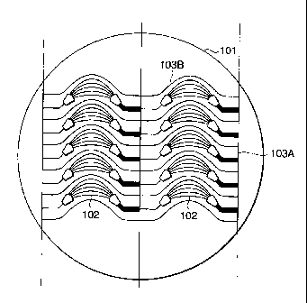
[0015] FIG. 4 shows arrayed waveguide grating elements formed on a
wafer according to the present invention. In FIG. 4, each arrayed waveguide
_g_
CA 02371630 2002-02-13
grating 102 has a shape similar to the shape shown in FIG. 1. Five arrayed
waveguide gratings 102 are formed in one row. Thus, ten arrayed waveguide
gratings 102 are formed in total. In each arrayed waveguide grating 102, the
portion corresponding to the channel waveguide array 14 (shown in FIG. 1) is
curved into an arcuate shape. Cutting paths 103A and 103B for cutting out an
individual arrayed waveguide grating chip are scribed so as to surround each
of
the arcuate or typical boomerang-shaped portions of the arrayed waveguide
gratings 102. The cutting paths 103 comprise straight cutting paths 103A and
curved cutting paths 103B. For the cutting paths 103B, two arcuate portions of
the same shape are arranged side by side in a lateral direction. Two arrayed
waveguide gratings 102 that are vertically adj acent to each other share a
conunon
curved cutting path 103B. That is, in contrast to the arrangement of arrayed
waveguide gratings shown in FIG. 2, the arrayed waveguide gratings 102 shown
in FIG. 3 are aligned in a vertically superimposed relationship, wherein
adjacent
patterns share a common curved-line portion (cutting path 103B). Accordingly,
the number of the arrayed waveguide grating chips that can be cut out from one
wafer 101 is considerably increased.
[0016] Note that, while cutting along the cutting paths 103A can be earned
out by dicing (since they are straight lines), dicing cannot be performed on
the
curved cutting paths 103B. Accordingly, in order to cut the wafer 1 O1 ShOWIl
lIl
FIG. 4, it is necessary to: (a) cut along the straight-line portions and
curved-line
portions by using a technique that allows cutting along a curved line; or (b)
use
the technique for cutting along a curved line and dicing in combination. The
_9_
CA 02371630 2002-02-13
following techniques exist for cutting a wafer along a curved line:
(1) Supersonic machining using a hom;
(2) Laser beam machining;
(3) Hydraulic machining; and
(4) Sandblast machining.
[0017] Among the above, the supersonic machining, laser beam machining
and hydraulic machining are well-knov~m techniques. However, when using laser
beam machining and hydraulic machining, it is necessary to trace of all the
cutting paths. Thus, these techniques are unsuitable for mass production
processes when the time required for the cutting operations is considered. For
mass production, it is preferable to use ultrasonic machining with a horn and
sandblast machining for the cutting operations. Note that sandblast machining
is a technique that is widely used for surface treatment. Sandblast machining
has
been used to perform surface treatment or removal of burrs from materials
other
than wafers, such as glass. Particles are blasted over the entire wafer, while
areas
of the wafer (other than those of cut out portions) are protected by coating a
resin
material or the like. This makes it possible to cut the wafer not only along a
straight line but also along a curved line.
[0018] The ultrasonic machining technique cuts a wafer by vibrating a tool
by means of ultrasonic waves transmitted via a resonant medium called a horn.
FIG. 5 shows the principle of cutting a wafer using ultrasonic machining. An
ultrasonic oscillator 121 is driven by alternating current to cause an
ultrasonic
vibrator 122 to vibrate and thereby generate ultrasonic waves. The ultrasonic
-10-
CA 02371630 2002-02-13
waves are transmitted via a cone 123 and a horn 124 to vibrate a tool 125 in a
vertical direction. A processing liquid 126, obtained by mixing abrasive
grains
in water, is supplied in a space between the tool 125 and the wafer 101 that
is to
be machined. At this point, when the tool 125 is being pressed against the
wafer
101 by applying appropriate pressure and ultrasonic vibration is generated,
the
wafer 101 is cut into a desired shape due to the impact of the abrasive grains
exerted thereon. Although the amount of machining achieved by each impact is
very small, since there are thousands of impacts per second, it is possible to
perform cutting along all the paths on the wafer 101 all at once by setting
the tip
of the tool 125 at a position to coincide with the cutting path 103 of the
wafer
101. Therefore, machining with high precision can be efficiently and quickly
performed. Needless to say, it is also possible to separate the cutting path
103
shown in FIG. 5 into a plurality of sub-cutting paths of the same shape in
advance, and to move the wafer 101 or the tool 125 along each of the separated
sub-cutting paths so that cutting is effected with respect to the each sub-
cutting
path by using the ultrasonic machining technique.
[0019) The clop manufacturuig process may include a step of inspecting the
characteristics of arrayed waveguide gratings on the individual chips obtained
by
cutting operations on the wafer 101. If the end-faces of the individual
arrayed
waveguides corresponding to the straight cutting paths do not form somewhat
fine mirror-finished surfaces at this stage, it is difficult to conduct an
optical
inspection that uses the end parts of input and output optical waveguides
existing
in these portions. Accordingly, when the precision of ultrasonic machining is
-11-
CA 02371630 2002-02-13
inadequate for carrying out such an inspection, it is effective to cut only
those
portions of the wafer corresponding to the cutting paths 103A by dicing so
that
a condition suitable for carrying out such inspection can be attained without
especially polishing the end-faces of the arrayed waveguide gratings.
[0020] FIG. 6 is used to explain how two different machining methods are
used depending on which portions of the wafer are being cut. First, ultrasonic
machining is performed along the curved cutting paths 103B. Next, dicing is
successively performed along the straight cutting paths 103A, so that each
arrayed waveguide grating 102 is cut from the wafer 101. Therefore, the
optical
characteristic test can be conducted without polishing the cut surfaces along
the
plane of the cutting paths 103A. Note that it is also possible to cut along
the
cutting paths 103A first. In that case, the optical characteristic test can be
conducted with respect to each arrayed waveguide grating 102 prior to cutting
along the curved cutting paths 103B.
[0021] FIG. 7 illustrates another layout example of arrayed waveguide
gratings provided on a wafer. According to FIG. 7, on the wafer 1 O1 A,
besides
the ten arrayed waveguide gratings 102 shown in FIG. 1, an inverted arrayed
waveguide gratings 102A is added. Thus, eleven arrayed waveguide gratings in
total can be cut from the wafer 101 A. In order to cut the arrayed waveguide
gratings from the wafer 101 A, the lower end portion of the straight cutting
path
103 A~ that is formed at the center must be terminated before reaclung the
pattern
102A. Therefore, in the case of the wafer 101 A shown in FIG. 7, dicing may be
applied to the straight cutting paths 103A2 and 103A3 arranged in the
peripheral
- 12-
CA 02371630 2002-02-13
portions. It is preferable, however, to use another cutting method with
respect to
the other cutting paths, such as ultrasonic machining. It is possible, of
course, to
cut along all of the cutting paths shown in FIG. 7 with ultrasonic machining
or
with sandblast machining.
(0022] As described above, the patterns of elements which are non-
rectangular in shape as a whole, such as arrayed waveguide gratings, are
efficiently laid out on a wafer, and then they are cut out in a given shape
that is
in conformity with the shape of each pattern. Therefore, a larger number of
chips
can be manufactured. However, as compared with a rectangular chip, the chips
cut out in this way may generally include a narrow-width region or a portion
of
weak mechanical strength, such as a small projecting portion. In the case of
the
arrayed waveguide grating, it has an arcuate or boomerang shape. Thus,
mechanical strength may deteriorate in portions having a reduced width
compared with related rectangular chips. The thickness of a chip, which
largely
affects its mechanical strength, is dependent upon the thickness of a silicon
wafer
or quartz glass as its main components. The thickness of an arrayed waveguide
grating chip is generally 1 ruin or less, which gives rather poor resistance
against
impact and vibration. It is necessary to ensure that an arrayed waveguide
grating
chip or an apparatus incorporating an arrayed waveguide grating chip is
capable
of fully withstanding any impacts that may be applied thereto. In order to
provide an arrayed waveguide grating clop (hereinafter abbreviated as an
arrayed
waveguide grating unless otherwise indicated) having excellent resistance
against
impact and vibration, it is necessary to: (i) improving the mechaucal strength
of
-13-
CA 02371630 2002-02-13
the arrayed waveguide grating chip itself; or (ii) provide a structure in
which
stresses are less likely to be imposed on the arrayed waveguide grating chip.
[0023] For improving the mechanical strength of the arrayed waveguide
grating chip itself, the following may be effective:
(a) Large copper plate: a copper plate that holds an arrayed waveguide
grating for heat dissipation is enlarged in size.
(b) Reinforcement beam: a reinforcement beam is attached to an arrayed
waveguide grating to enhance its mechanical strength.
(c) Two-layer substrate structure: a silicon substrate having the same shape
as the arrayed waveguide grating is prepared and attached to the arrayed
waveguide grating, thereby increasing the overall thickness.
[0024] As for providing a structure in which stresses are less likely to be
applied on the chip, the following may be effective.
(d) Buffer filling type: buffer agents (heat insulating material) are filled
within a package for accommodating an arrayed waveguide grating.
(e) Supporting by spring type: edge portions of an arrayed waveguide
grating are fixed by means of spring members to thereby absorb impact applied
thereon.
[0025] By employing an enlarged heat dissipation copper plate for holding
an arrayed waveguide grating, resistance of a wafer against impact or
vibration
is enhanced. FIG. 8 shows an interior of a package for accommodating an
arrayed waveguide grating. An arrayed waveguide grating package 201
comprises a hollow box-like case comprised of a case bottom plate portion 202
- 14-
CA 02371630 2002-02-13
and a case cover 203. In the case bottom plate portion 202, a tabular heater
205
is disposed in parallel to the case bottom plate portion 202 through heat
insulating
columns 204. A large copper plate 206 is placed on the heater 205, and an
arrayed waveguide grating 207 is mounted on the large copper plate 206.
Although not shown, a groove is etched in the surface of the large copper
plate
206 opposing the arrayed waveguide grating 207, which extends from a
peripheral portion of the surface to a central portion thereof. A temperature
detecting element 208 is embedded in the portion of the groove corresponding
to
the portion of the chamiel waveguide array 14 of the arrayed waveguide grating
207. A lead wire of the temperature detecting element 208 is embedded in the
other portion of the groove. The temperature detecting element 208 detects the
temperature of the heater 205 and adjusts the temperature of the arrayed
waveguide grating 207 to a desired temperature. Optical fibers 211 and 212 are
introduced into the arrayed waveguide grating package 201. Each of the optical
fibers 211 and 212 is connected to an external apparatus (not shown). The
optical
fiber 211 is fixed to an edge portion of the arrayed waveguide grating 207 by
an
ultraviolet curing adhesive. The optical fiber 212 is fixed to a fiber array
(not
shown) of the arrayed waveguide grating 207.
[0026] FIG. 9 shows an arrayed waveguide grating 207 according to the
present embodiment mounted on the large copper plate 206, as seen from the
above within the package. Preferably, the large copper plate 206 is tough
pitch
copper as defined by C 1100 of the JIS standards is used as a copper material
having excellent workability. The large copper plate 206 has a rectangular
shape
-15-
CA 02371630 2002-02-13
of 6 x 4 cm substantially surrounding the arrayed waveguide grating 207, and
is formed with a thickness of several millimeters. The arrayed waveguide
grating
207 is mounted to the large copper plate 206. Copper materials other than
tough
pitch copper may also be used. By way of reference, FIG. 10 shows an example
of an arrayed waveguide grating and a copper plate employed in a related
arrayed
waveguide grating package. A rectangular area indicated by a dashed line
within
a rectangular shaped array waveguide chip 221 is the area occupied by a copper
plate 222. The large copper plate 206 shown in FIG. 9 is larger in size than
the
copper plate 222 shown in FIG. 10. Consequently, the weak mechanical strength
of the peripheral portion of the arrayed waveguide grating 207 is enhanced. By
way of reference, FIG. 11 shows an arrayed waveguide grating having an arcuate
profile in accordance with the present invention mounted to a related copper
plate. Here, there is assumed a model structure in which loads equivalent to
those
of fiber arrays 231 and 232 are applied onto the free ends of a cantilever
beam of
6 mm in width, 0.83 mm in thickness, and 27 mm in length. According to the
model structure, a cantilever beam capable of withstanding impact of 500 G
must
be backed with three or more silicon substrates having the same thickness and
configuration as those of the arrayed waveguide grating. Although a large
rectangular copper plate is used, a copper plate having the same configuration
as
the arrayed waveguide grating 207 can also be used by bonding it onto the
arrayed waveguide grating 207.
[0027] Alternatively, using a reinforcement beam provides excellent
resistance against impact and vibration. FIG. 12 shows an example of an
arrayed
- 16-
CA 02371630 2002-02-13
waveguide grating using reinforcement beams. In an arrayed waveguide grating
207A, reinforcement beams 251 and 252 are respectively attached to a rise
portion and a fall portion of the arcuate shape. The reinforcement beams 251
and
252 are symmetrical with respect to the center axis 253 of the arrayed
waveguide
grating 207A.
[0028] A two-layer substrate structure also provides excellent resistance
against impact and vibration. FIG. 13 shows an . example of an arrayed
waveguide grating having a two-layer substrate structure. An arrayed waveguide
grating 207B is obtained by boding together the arrayed waveguide grating 207
shown in FIGS. 9 and 11 and a silicon substrate 271 of an arcuate shape having
the same size and configuration as that of the silicon substrate 207 with
adhesives (not shown in FIG. 13). FIG. 14 shows a wafer from which the silicon
substrate having an arcuate shape is cut out. The same cutting paths 103A and
103B as those in the wafer 101 shown in FIG. 4 are scribed on a wafer 272.
Since there is no need to provide the arrayed waveguide grating 207 shown in
FIG. 4 on this wafer 272, a wafer having a purity level of silicon lower than
that
of the wafer 101 may be used as the wafer 272. Moreover, since the entire
manufacturing process of the arrayed waveguide grating 207 itself is
unnecessary,
each arcuate-shaped silicon substrate 271 may be manufactured quite
inexpensively. Therefore, the arrayed waveguide grating 207B having a two-
layer substrate structure as shown in FIG. 13 may be manufactured at
considerably less manufacturing cost as compared with the arrayed waveguide
grating having a rectangular shape used in the prior art. In FIG. 13, instead
of the
-17-
CA 02371630 2002-02-13
arrayed waveguide grating 207B having the two-layer substrate structure, it is
also possible to manufacture an arrayed waveguide grating having a mufti-layer
substrate structure by bonding together two or more arcuate-shaped silicon
substrates 271. Further, the thickness of the wafer 272 from which the arcuate-
shaped silicon substrates are cut out may be made sufficiently larger than
that of
the arrayed waveguide grating 207 to enhance its mechanical strength.
[0029] Buffer filling also provides excellent resistance against impact and
vibration. FIG. 15 shows an example of interior structure of an array
waveguide
grating package for an arrayed waveguide grating of a buffer filling type. In
FIG.
15, the same or identical parts as those in FIG. 8 are represented by the same
symbols, and explanation thereof is omitted here. As will be noted from
comparison with FIG. 8, in the arrayed waveguide grating package 201A
according to this modification, a first buffer and heat insulating agent 291
is filled
in the space above the arrayed waveguide grating 207, a second buffer and heat
insulating agent 292 is filled in the space below an optical fiber 211 defined
by
a heat insulating column 204 and a case cover 203, and a third buffer and heat
insulating agent 293 is filled in the space below an optical fiber 212 defined
by
the other heat insulating column 204 and the case cover 203. These first to
third
buffer and heat insulating agents 291, 292 and 293 may be prepared by
processing various materials having elasticity that have been used as
insulating
materials into appropriate forms.
[0030] FIG. 16 shows another exemplary interior structure of an arrayed
waveguide grating package for an arrayed waveguide grating with buffer filling
-18-
CA 02371630 2002-02-13
material. In FIG. 16, the same or identical parts as those in FIG. 8 are
represented
by the same symbols, and explanation thereof is omitted here. In contrast to
the
arrayed waveguide grating package shown in FIG. 8, the arrayed waveguide
grating package 201B is provided with a plurality of lower columns 301 made of
spring material, instead of the heat insulating columns 204. Further, a
plurality
of upper columns 302 are also arranged between the upper surface of the
arrayed
waveguide grating 207 and the rear surface of the upper portion of the case
cover
203. Preferably, these columns 301 and 302 have excellent insulating
properties,
in addition to excellent spring properties. Since the arrayed waveguide
grating
207 is elastically supported by the upper and lower columns 301 and 302 in the
arrayed waveguide grating package 201B, impact forces applied to the exterior
of the package can be effectively absorbed. An elastic member for absorbing
impact in a lateral direction may also be arranged on the case bottom plate
portion 202 or the case cover 203.
[0031] The foregoing description is directed to an arrayed waveguide
grating chip having an arcuate shape. Needless to say, however, the present
invention can be applied to all types of chips having a non-rectangular
profile or
having a contour of a predetermined closed loop shape including a curved line
at
least in a part thereof.
[0032] FIG. 17 is a layout view of 1 X N splitters on a wafer. The example
given here is different from the above-described embodiments in that six 1 X N
sputters 333 each having a funnel shape obtained by dividing a rhombus in half
are arranged on a wafer 1 O1 B. In comparison with FIG. 3, three times more
clops
-19-
CA 02371630 2002-02-13
having the same shape and size can be obtained from one wafer lOIB.
[0033] As described above, the present invention, the individual chips are
not formed in a uniform rectangular shape as in the prior art, but are formed
in
a concave shape wherein unnecessary portions are removed. Consequently, the
number of chips that can be obtained from one wafer is increased, thus
allowing
corresponding reduction in cost.
[0034] Obviously, numerous additional modifications and variations of the
present invention are possible in light of the above teachings. It is,
therefore, to
be understood that within the scope of the appended claims, the invention may
be practiced otherwise than as specifically described herein.
-20-