Note: Descriptions are shown in the official language in which they were submitted.
CA 02372080 2001-10-12
t
DESCR=hT=ON
SEI 99-48
OPTICAL TRANSMITTER AND OPTICAL COMMUNICATION SYSTEM
PROVIDED THEREWITH
Technical Field
The present invention relates to an optical
transmitter for outputting light signals to an optical
transmission line and an optical communication system
provided therewith.
Background Art
The common optical communication systems are
provided with an optical transmitter for outputting
light signals, an optical transmission line, such as an
optical fiber or the like, for transmitting the light
signals, and an optical receiver for receiving the
light signals having propagated through this optical
transmission line. It is generally known as to the
optical transmission lines such as the optical fibers
that the nonlinear optical phenomena become easier to
occur in the optical transmission line when the power
of light signals propagating therethrough is high. It
is also known that the nonlinear optical phenomena
degrade the waveform of light including signals, so as
to tend to cause reception errors at the optical
receiver. For this reason, it is an important subject
1
CA 02372080 2001-10-12
' SEI 99-48
in the field of the optical communication systems to
restrain occurrence of the nonlinear optical phenomena
and thereby prevent the degradation of the waveform of
light including signals.
There are a variety of nonlinear optical
phenomena known as those occurring in the optical
fibers, one of which is the stimulated Brillouin
scattering (which will be referred hereinafter as SBS).
For example, Reference 1: Y. K. Park et al., "A 5Gb/s
Repeaterless Transmission System Using Erbium-Doped
Fiber Amplifiers," IEEE Photon. Technol. Lett., Vol. 5,
No. 1, pp.79-82 (1993) describes the result of
experiments to investigate the relationship between
occurrence of SBS and degradation of transmission
characteristics.
As techniques for restraining the occurrence of
SBS there are, for example, the techniques described in
Reference 2: S. K. Korotky et al., "Efficient Phase
Modulation Scheme for Suppressing Stimulated Brillouin
Scattering," IOOC '95, WD2-1 (1995), Reference 3: D. A.
Fishman et al., "Degradations Due to Stimulated
Brillouin Scattering in Multigigabit Intensity-
Modulated Fiber-Optic System," J. Lightwave Technol.,
Vol. 11, No. 11, pp.1721-1728 (1993), Reference 4: T.
Sugie, "Transmission Limitations of CPFSK Coherent
Lightwave Systems Due to Stimulated Brillouin
2
CA 02372080 2001-10-12
SEI 99-48
Scattering in Optical Fiber," J. Lightwave Technol.,
Vol. 9, No. 9, pp.1145-1155 (1991), and Reference 5: L.
Eskildsen et al., "Stimulated Brillouin scattering
suppression with low residual AM using a novel
temperature wavelength-dithered DFB laser diode,"
Electron. Lett., Vol. 32, No. 15, pp.1387-1388 (1996),
and so on.
The SBS suppression techniques described in
these References 2 to 5 are fundamentally the
technology for suppressing the occurrence of SBS by
phase modulation or frequency modulation of laser light
emitted from a semiconductor laser as a light source.
The phase-modulated or frequency-modulated laser light
is outputted as light including signals to the optical
transmission line after high-frequency signal
components are superimposed thereon. The SBS
suppression technique described in above Reference 5 is
the technology of adequately reducing amplitude
modulation of the laser light emitted from the
semiconductor laser source by minimizing amplitude
modulation caused during the phase modulation. In the
semiconductor laser source, the phase modulation or
frequency modulation of the laser light is effected by
varying the refractive index of an active layer
according to bias or driving current modulated by a
modulation signal source, and thus it also brings about
3
CA 02372080 2001-10-12
' SEI 99-48
unintended amplitude modulation at the same time.
Therefore, Reference 5 discloses the semiconductor
laser source provided with special structure for
suppressing the amplitude modulation caused during the
phase modulation.
Disclosure of the Invention
The inventor investigated the above-stated prior
arts and found the following issue. Namely, as
illustrated in Fig. 1, the period of the amplitude
modulation over the light including signals is equal to
the period 1/fm of the phase modulation or frequency
modulation. In this Fig. 1, the average power of the
laser light emitted from the semiconductor laser source
is indicated by P1 and the power amplitude of the laser
light by al. The modulation depth is defined as al/P1.
If the laser light emitted with the driving
current supplied to the semiconductor laser source does
not undergo direct modulation, the spectrum of the
laser light emitted from the semiconductor laser source
will be one having the shape of a narrow bandwidth
around the frequency fo, as illustrated in Fig. 2A. If
the laser light emitted with the driving current
supplied to the semiconductor laser source undergoes
direct modulation on the other hand, the spectrum of
the laser light emitted from the semiconductor laser
source will be one having the shape of a broad
4
CA 02372080 2001-10-12
' ' SEI 99-48
bandwidth around the frequency fo, as illustrated in
Fig. 2B, because of occurrence of chirping due to
variation in the refractive index of the waveguide
layer in the semiconductor laser source. Then this
expansion of the spectral width of laser light makes it
possible to suppress the occurrence of SBS.
In the conventional optical communication systems,
since the power of the laser light from the
semiconductor laser source is low, it is common
practice to amplify the laser light once by an optical
amplifier and thereafter output the amplified light to
the optical transmission line. The light including
signals having passed through the optical amplifier
(the amplified laser light), as illustrated in Fig. 3,
has the average optical power Pz larger than the
average optical power P1 of the laser light emitted
from the semiconductor laser source, the power
amplitude of az (> al), and the modulation depth of
az/Pz. It is noted here that the modulation components
from the signal source is omitted from this waveform
illustrated in Fig. 3.
Therefore, the light including signals outputted
from the optical amplifier to the optical transmission
line can be regarded as amplitude-modulated light
having the average optical power of Pz and the
amplitude of az, and the maximum optical power PmaX
5
CA 02372080 2001-10-12
SEI 99-48
thereof is given by P2 + a2. If this maximum optical
power Pmax exceeds a predetermined threshold (Fig. 4A
shows a state in which the maximum optical power PmaX is
over the predetermined threshold L1 in the region
indicated by A and Fig. 4 also includes an illustration
of the signal components, unlike Fig. 3), the nonlinear
optical phenomena, such as four-wave mixing, Self-Phase
Modulation (SPM), etc., will become prominent in the
optical transmission line and, as illustrated in Fig.
4B, the signal light after propagation through the
long-haul optical transmission line will demonstrate
considerable degradation of the waveform due to
influence of dispersion in the optical transmission
line. This will result in alternate appearance of
regions with heavy waveform degradation (regions as
indicated by A in Fig. 4A and Fig. 4B) and regions with
little waveform degradation in the period of 1/fm on
the time axis in the conventional optical communication.
The present invention has been accomplished in
order to solve the above-stated issue and an object of
the present invention is thus to provide an optical
transmitter having the structure for enabling output of
high-power light signals while effectively suppressing
occurrence of the nonlinear optical phenomena,
particularly, SBS, and an optical communication system
equipped therewith.
6
CA 02372080 2001-10-12
SEI 99-48
An optical transmitter according to the present
invention is characterized by comprising a modulation
signal source for outputting modulation signals of a
predetermined frequency, a semiconductor laser source
driven by the modulation signals from the modulation
signal source to output laser light modulated according
to the modulation signals, an optical amplifier for
amplifying the laser light from the semiconductor laser
source, and a modulation depth control system for
controlling a ratio of an amplitude modulation depth of
amplified laser light outputted from the optical
amplifier, to an amplitude modulation depth of the
laser light inputted into the optical amplifier in the
range of 60$ or less, preferably, in the range of 10$
or less.
In the above-stated structure the modulation
signal source for supplying the electric signals for
driving the above semiconductor laser source is
utilized as a signal source for supplying signals to be
superimposed on the laser light, but the optical
transmitter may also be constructed in structure
further comprising a signal source for outputting
signals to be transmitted, in the form of an electric
signal, and an external modulator which is disposed on
a transmission line between the semiconductor laser
source and the optical amplifier, which amplitude-
7
CA 02372080 2001-10-12
' SEI 99-48
modulates the laser light outputted from the
semiconductor laser source, based on the electric
signals outputted from the signal source, and which
outputs the amplitude-modulated laser light as light
including signals to the optical amplifier. The above
optical amplifier may comprise an erbium-doped optical
fiber. In this case, since the response characteristic
of population inversion is relatively low in the
amplifying optical fiber, the modulation frequency in
the modulation signal source is more preferably in the
range of 20 kHz or less.
In this way, the laser light outputted from the
semiconductor laser source is amplitude-modulated by
the modulation signals of the predetermined frequency
(preferably, 20 kHz or les s , the high-frequency signal
components are superimposed thereon to form the light
including signals (in the case of the structure having
the external modulator, the signal components are
superimposed on the laser light by the external
modulator in accordance with the electric signals from
the signal source), and these light signals is
amplified by the optical amplifier. In the optical
transmitter according to the present invention, since
the modulation depth control system controls the
amplitude modulation depth of the amplified laser light
outputted from the optical amplifier in the range of
8
CA 02372080 2001-10-12
SEI 99-48
60$ or less, preferably, in the range of 10% or less of
the amplitude modulation depth of the laser light
inputted into the optical amplifier, the maximum
optical power Pn,ax of the laser light outputted from the
optical amplifier can be kept at or below the level L1
where the waveform degradation becomes unignorable due
to the nonlinear optical phenomena (see Fig. 4A) and it
can effectively suppress the occurrence of the
nonlinear optical phenomena, particularly, SBS in the
optical transmission line placed after the optical
transmitter while enabling output of high-power light
signals.
In the optical transmitter according to the
present invention, the aforementioned modulation depth
control system controls either one of a driving system
of the semiconductor laser source and a time response
element of the optical amplifier, thereby controlling
the amplitude modulation depth of the amplified laser
light outputted from the optical amplifier in the range
of 60~ or less, preferably, in the range of 10$ or less
of the amplitude modulation depth of the laser light
inputted into the optical amplifier. Specifically, the
control operation over the driving system of the
semiconductor laser source can be implemented by a
control operation to control the modulation frequency
to the semiconductor laser source and the signal
9
CA 02372080 2001-10-12
SEI 99-48
intensities of the driving signals, and the control
operation over the time response element of the optical
amplifier by a control operation to control a parameter
i (response speed of population inversion) of the
amplifying optical fiber in the optical amplifier (i.e.,
by selection of the amplifying optical fiber applied to
the optical amplifier), or by a control operation to
control a time constant of a circuit element in the
optical amplifier.
An optical communication system according to the
present invention comprises the above-stated optical
transmitter for outputting light signals, an optical
transmission line through which the light signals
outputted from the optical transmitter propagates, and
an optical receiver for receiving the light signals
having propagated through the optical transmission line.
In this optical communication system, the light signals
outputted from the optical transmitter travels through
the optical transmission line to the optical receiver
to be received thereby. Since the above-stated optical
transmitter is applied to this system, it can suppress
the occurrence of the nonlinear optical phenomena,
particularly, SBS in the optical transmission line and
transmit the light signals of high power, thus
decreasing the reception errors at the optical receiver.
Each of the embodiments of the present invention
CA 02372080 2001-10-12
SEI 99-48
can be fully understood by the detailed description and
accompanying drawings which follow. These embodiments
should be considered to be simply illustrative but not
restrictive for the invention.
The scope of further application of the present
invention will become apparent by the detailed
description of the invention which follows. However,
the detailed description and specific examples are
given for describing the preferred embodiments of the
present invention, and are presented only for
illustration, and it is obvious that various
modifications and improvements within the spirit and
scope of the present invention are apparent to those
who are skilled in the art from the detailed
description.
Brief Description of the Drawings
Fig. 1 is a drawing for explaining the waveform
of the laser light (light including signals) outputted
from the semiconductor laser source.
Fig. 2A and Fig. 2B are drawings for explaining
the spectra of the laser light outputted from the
semiconductor laser source.
Fig. 3 is a diagram for explaining the waveform
of the laser light amplified by the optical amplifier.
Fig. 4A is a diagram to show the waveform of the
light including signals accompanied by the data signals
11
CA 02372080 2001-10-12
' ' SEI 99-48
to be outputted from the optical amplifier to the
optical transmission line, and Fig. 4B a diagram for
explaining the waveform of light including signals
after long-haul transmission.
Fig. 5A is a diagram to show the structure of the
first embodiment of the optical transmitter and the
optical communication system provided therewith
according to the present invention, and Fig. 5B a
diagram to show the structure of the second embodiment
of the optical transmitter and the optical
communication system provided therewith according to
the present invention.
Fig. 6A to Fig. 6C are diagrams to show the
waveforms of the light including signals at the input
end and at the output end of the optical amplifier
where the modulation frequency is low, wherein Fig. 6A
shows the optical amplifier, Fig. 6B the waveform of
the light including signals at the part indicated by A1
(i.e., at the input end) in Fig. 6A showing the optical
amplifier, and Fig. 6C the waveform of the light
including signals at the part indicated by B1 (i.e., at
the output end) in Fig. 6A showing the optical
amplifier.
Fig. 7A to Fig. 7C are diagrams to show the
waveforms of the light including signals at the input
end and at the output end of the optical amplifier
12
CA 02372080 2001-10-12
SEI 99-48
where the modulation frequency is high, wherein Fig. 7A
shows the optical amplifier, Fig. 7B the waveform of
the light including signals at the part indicated by A2
(i.e., at the input end) in Fig. 7A showing the optical
amplifier, and Fig. 7C the waveform of the light
including signals at the part indicated by B2 (i.e., at
the output end) in Fig. 7A showing the optical
amplifier .
Fig. 8A and Fig. 8B are diagrams to show spectra
of the laser light where the modulation frequency is 1
kHz and the modulation depth is 20%, wherein Fig. 8A is
a diagram to show the laser light spectrum before input
into the optical amplifier and Fig. 8B a diagram to
show the laser light spectrum after passage through the
optical amplifier.
Fig. 9A and Fig. 9B are diagrams to show spectra
of the laser light where the modulation frequencies are
7 kHz and 20 kHz and the modulation depth is 20%,
wherein Fig. 9A is a diagram to show the laser light
spectrum before input into the optical amplifier and
Fig. 9B a diagram to show the laser light spectrum
after passage through the optical amplifier.
Fig. l0A and Fig. lOB are diagrams to show the
time waveforms of the laser light where the modulation
frequency is 1 kHz and the modulation depth is 10%,
wherein Fig. l0A is a diagram to show the time waveform
13
CA 02372080 2001-10-12
SEI 99-48
of the laser light before input into the optical
amplifier and Fig. lOB a diagram to show the time
waveform of the laser light after passage through the
optical amplifier.
Fig. 11A and Fig. 11B are diagrams to show the
time waveforms of the laser light where the modulation
frequency is 40 kHz and the modulation depth is 10~,
wherein Fig. 11A is a diagram to show the time waveform
of the laser light before input into the optical
amplifier and Fig. 11B a diagram to show the time
waveform of the laser light after passage through the
optical amplifier.
Fig. 12 is a graph to show an example of
relationship between modulation frequency and
modulation depth.
Fig. 13 is a graph to show the relationship
between optical power (incident optical power) of the
light including signals outputted from the optical
amplifier to the optical transmission line and optical
power (reflected optical power) of the reflected
components from the optical transmission line.
Best Mode for Carrying out the Invention
The optical transmitters and optical
communication systems according to the present
invention will be described hereinafter with reference
to Fig. 5A to Fig. 11B, Fig. 12, and Fig. 13. In the
14
CA 02372080 2001-10-12
SEI 99-48
description of the drawings like elements will be
denoted by the same reference symbols and redundant
description will be avoided.
Fig. 5A is a diagram to show the structure of the
first embodiment of the optical transmitter and the
optical communication system provided therewith
according to the present invention, and the optical
communication system according to the first embodiment
is provided with an optical fiber transmission line 20,
an optical transmitter l0a disposed on the input end
side of the optical fiber transmission line 20, and an
optical receiver 30 disposed on the output end side of
the optical fiber transmission line 20. In this first
embodiment, the optical transmitter l0a is constructed
to perform the modulation operation over the laser
light of a carrier wave and the superposition operation
of the signal components simultaneously and,
specifically, the optical transmitter l0a comprises a
modulation signal source 11 functioning to output the
modulation signals of the frequency fm and also
functioning as a signal source, a semiconductor laser
source 12 (LD) for outputting the laser light
(including the signal components) phase-modulated or
frequency-modulated and also amplitude-modulated, based
on the modulation signals, an optical amplifier 13 for
amplifying the laser light outputted from the
CA 02372080 2001-10-12
' ' SEI 99-48
semiconductor laser source 2, as light including
signals, and a modulation depth control system for
controlling the amplitude modulation depth of the
amplified laser light outputted from the optical
amplifier in the range of 60~ or less, preferably, in
the range of 10~ or less of the amplitude modulation
depth of the laser light inputted into the optical
amplif ier .
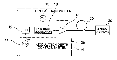
On the other hand, Fig. 5B is a diagram to show
the structure of the second embodiment of the optical
transmitter and the optical communication system
provided therewith according to the present invention,
and the optical communication system according to the
second embodiment is provided with the optical fiber
transmission line 20, the optical transmitter lOb
disposed on the input end side of the optical fiber
transmission line, and the optical receiver 30 disposed
on the output end side of the optical fiber
transmission line 20. In this second embodiment, the
optical transmitter lOb is constructed of separate
mechanisms for outputting the laser light of the
carrier wave and for superimposing the high-frequency
signals thereon and, specifically, it has the
modulation signal source 11, the semiconductor laser
source 12 (LD), the optical amplifier 13, and the
modulation depth control system 14 and further has a
16
CA 02372080 2001-10-12
' ' SEI 99-48
signal source 15 for outputting the signals to be
transmitted, in the form of an electric signal, and an
external modulator 16 which is disposed on the
transmission line between the semiconductor laser
source 12 and the optical amplifier 13, which
amplitude-modulates the laser light outputted from the
semiconductor laser source 12, based on the electric
signals outputted from the signal source 15, and which
outputs the amplitude-modulated laser light as the
light including signals to the optical amplifier 13.
The modulation signal source 11 outputs the
modulation signals of the frequency fm, for example, 20
kHz or less to the semiconductor laser source 12. The
semiconductor laser source 12 is driven by the
modulation signals of the frequency fm outputted from
the modulation signal source 11 and outputs the laser
light amplitude-modulated while phase-modulated or
frequency-modulated according to the modulation signals.
The wavelength band of this laser light is preferably
the 1.55wm wavelength band, for example. The signal
source 15 outputs the signal components to be
transmitted, in the form of the electric signal. The
external modulator 16 amplitude-modulates the laser
light outputted from the semiconductor laser source 12,
based on the electric signal outputted from the signal
source 15, and outputs the amplitude-modulated laser
17
CA 02372080 2001-10-12
' SEI 99-48
light as the light including signals.
The optical amplifier 13 amplifies the signal
light outputted from the external modulator 16 and
outputs the amplified light including signals to the
optical transmission line 20. Particularly, the
optical amplifier 13 is preferably an erbium-doped
optical fiber amplifier which has an amplifying optical
fiber with the core region doped with the element Er or
the like, and a pumping source for supplying pumping
light of a predetermined wavelength to the amplifying
optical fiber. The reason is that it becomes easier to
control the modulation depth of the light including
signals outputted from the optical amplifier 13,
because the response characteristic of population
inversion is relatively low in the amplifying optical
fiber where the optical amplifier 13 is the erbium-
doped optical fiber amplifier.
Here the modulation depth control system 14
controls at least either one of the driving system
(modulation signal source 11) of the semiconductor
laser source 12 and the time response element of the
optical amplifier 13, thereby controlling the amplitude
modulation depth of the amplified laser light
(frequency fm) outputted from the optical amplifier in
the range of 60~ or less, preferably, in the range of
10~ or less of the amplitude modulation depth of the
18
CA 02372080 2001-10-12
' ' SEI 99-48
laser light inputted into the optical amplifier.
Then the signal light outputted from the optical
amplifier 13 of the optical transmitter lOb propagates
through the optical transmission line 20 to reach the
optical receiver 30. The optical receiver 30 receives
these light signals thus arriving. In the structure as
described above, the signal light can be transmitted
from the optical transmitter 10 through the optical
transmission line 20 to the optical receiver 30 with
effectively suppressing the occurrence of SBS and
avoiding the degradation of the signal waveform, even
in high-speed optical transmission over 1 Gbs.
In the conventional optical communication systems,
where the optical power is 7 dBm or more for the light
signals outputted from the optical transmitter 10 to
the optical transmission line 20, the occurrence of
nonlinear optical phenomena becomes conspicuous in the
optical transmission line 20. However, in the case of
the optical transmitters 10a, lOb having their
respective structures according to the embodiments, the
occurrence of SBS can be effectively restrained (the
waveform degradation of light including signals can be
avoided) even if the optical power of the light
including signals outputted to the optical transmission
line 20 is 7 dBm or mare.
Further, in the conventional optical
19
CA 02372080 2001-10-12
' ' SEI 99-48
communication systems, even if the value of <N2>/Aeff is
6 x 10⁻¹°/W or more at the input end of the optical
transmission line 20 where <N2> is a nonlinear
refractive index of the optical fiber of the optical
transmission line 20 and Aaff is an effective area, the
occurrence of nonlinear optical phenomena becomes
conspicuous in the optical transmission line 20. In
contrast with it, the optical transmitters 10a, lOb
according to the present invention can effectively
suppress the occurrence of SBS even if the value of
<N2>/Aeff is 6 x 10⁻¹°/W or more at the input end of the
optical transmission line 20.
The refractive index <N> of the medium under
strong light varies depending upon the light intensity
as described above. Therefore, the lowest-order effect
on this index <N> is expressed by the following
equation:
<N> _ <NO> + <N2>.~E~2
where <NO>: refractive index for linear
polarization;
<N2>: second-order nonlinear refractive index for
nonlinear polarization; and
~E~2~ light intensity.
Namely, under strong light, the refractive index <N> of
CA 02372080 2001-10-12
' ' SEI 99-48
the medium is given by the sum of the normal value <NO>
and an increase proportional to the square of the
amplitude E of the electric field of the light.
Particularly, the proportional constant <N2> of the
second term (unit: mz/W) is called the second-order
nonlinear refractive index. Since distortion of signal
pulses is affected mainly by the second-order nonlinear
refractive index out of the nonlinear refractive
indexes, the nonlinear refractive index stated in the
present specification mainly means this second-order
nonlinear refractive index.
In addition, the aforementioned effective area
Aeff 1S given by the following equation, as described in
Japanese Patent Application Laid-Open No. 8-248251
(EP0724171A2).
m
Ae~ = 2,n(J'EZrdr)2 /{ f E4rdr)
0 0
In this equation, E represents the electric field
caused by the propagating light and r the radial
distance from the center of the core.
Now let us describe in detail how the present
invention has been accomplished.
With input of the light signals to the optical
amplifier 13, the response of the optical amplifier 13
21
CA 02372080 2001-10-12
SEI 99-48
to the modulation waveform (the modulation components
of the frequency fm from the modulation signal source
11) of the inputted light including signals is reduced
to temporal behavior of population inversion (gain
coefficient) in the laser medium of the optical
amplifier 13 upon input of light signals. The response
speed of population inversion in the laser medium of
the optical amplifier 13 is dominated by the effective
lifetime ieff of the higher energy state of the laser
medium expressed by the following equation.
2eff - ~~( 1 ~' I~IS + Ip~Ipth)
In this equation, i is the lifetime of the higher
energy state in the amplifying optical fiber under
absence of light, I the intensity of the inputted light
including signals, Ia the saturation intensity of the
inputted light including signals, Ip the intensity of
the pumping light, and Ipth the threshold intensity of
the pumping light where the laser medium of the optical
amplifier 13 becomes transparent.
When the frequency fm of the amplitude modulation
(the modulation components from the modulation signal
source 11) of the light including signals inputted into
the optical amplifier 13 is relatively low, i.e., when
the period 1/fm of the amplitude modulation is longer
22
CA 02372080 2001-10-12
SEI 99-48
than the effective lifetime ieff of the higher energy
state, the population inversion (gain coefficient) in
the optical amplifier 13 can follow variation in the
intensity of the light including signals inputted into
the optical amplifier 13. As a consequence, the light
including signals outputted from the optical amplifier
13 demonstrates a decrease of the modulation depth; the
modulation depth at the input end is decreased to that
at the output end, as illustrated in Fig. 6B and Fig.
6C, or the modulation amplitude becomes almost zero
(continuous light). Fig. 6B is a diagram to show the
waveform of the light including signals at the part
(input end) indicated by A1 in Fig. 6A showing the
optical amplifier, and Fig. 6C a diagram to show the
waveform of the light including signals at the part
(output end) indicated by B1 in Fig. 6A.
On the other hand, when the frequency fm of the
amplitude modulation (the modulation components from
the modulation signal source 11) of the light including
signals inputted into the optical amplifier 13 is
relatively high, i.e., when the period 1/fm of the
amplitude modulation is shorter than the effective
lifetime -c~ff of the higher energy state, the population
inversion (gain coefficient) in the optical amplifier
13 becomes unable to follow the variation in the
intensity of the inputted light including signals, so
23
CA 02372080 2001-10-12
SEI 99-48
that the optical amplifier 13 comes to have an almost
constant gain coefficient according to the average
intensity of the inputted light including signals. As
a consequence, as illustrated in Fig. 7B and Fig. 7C,
the modulation depth of the light including signals
outputted from the optical amplifier 13 becomes almost
equal to that of the light including signals inputted
into the optical amplifier 13. Fig. 7B is a diagram to
show the waveform of the light including signals at the
part (input end) indicated by A2 in Fig. 7A showing the
optical amplifier, and Fig. 7C a diagram to show the
waveform of the light including signals at the part
(output end) indicated by B2 in Fig. 7A showing the
optical amplifier. It is noted that the modulation
components (signal components) from the signal source 3
is omitted from the illustration of the waveform in
each of above Fig. 6B, Fig. 6C, Fig. 7B, and Fig. 7C.
As apparent from the above equation concerning
the effective lifetime i~ff of the higher energy state,
while the intensity I of the light including signals
inputted into the optical amplifier 13 is sufficiently
smaller than the saturation intensity I8, the change of
the intensity I of the light including signals makes
little contribution to the value of the effective
lifetime teff of the higher energy state (or is
negligible). However, when the intensity I of the
24
CA 02372080 2001-10-12
SEI 99-48
inputted light including signals becomes approximately
equal to or larger than the saturation intensity Is,
i.e., when the optical amplifier 13 is operated near
the saturation intensity, the change of the intensity I
of the inputted light including signals comes to make
great contribution to the value of the effective
lifetime ieff of the higher energy state. Therefore,
the occurrence of SBS in the optical transmission line
will pose a problem in the ordinary optical
communication systems in which the optical amplifier 13
is operated near the saturation intensity.
The inventor proved the above-stated phenomena by
experiments. Fig. 8A and Fig. 8B are diagrams to show
the spectra of the laser light where the modulation
frequency fm is 1 kHz and the modulation depth is 20~,
wherein Fig. 8A is a diagram to show the laser light
spectrum before input into the optical amplifier 13
(the spectrum of the light including signals before
amplification) and Fig. 8B a diagram to show the laser
light spectrum after passage through the optical
amplifier 13 (the spectrum of the light including
signals after amplification). As seen from these
diagrams, the sideband component corresponding to the
modulation frequency fm disappeared from the light
including signals outputted from the optical amplifier
13.
CA 02372080 2001-10-12
SEI 99-48
Fig. 9A and Fig. 9B are diagrams to show laser
light spectra where the modulation frequencies fm are 7
kHz and 20 kHz and the modulation depth is 20$, wherein
Fig. 9A is a diagram to show the laser light spectrum
before input into the optical amplifier 13 (the
spectrum of the light including signals before
amplification) and Fig. 9B a diagram to show the laser
light spectrum after passage through the optical
amplifier 13 (the spectrum of the light including
signals after amplification). As seen from these
figures, the component of the modulation frequency of 7
kHz disappeared but the components of the modulation
frequency of 20 kHz remained in the light including
signals outputted from the optical amplifier 13.
Further, Fig. l0A and Fig. 10B are diagrams to
show the time waveforms of the laser light where the
modulation frequency fm is 1 kHz and the modulation
depth is 10%, wherein Fig. l0A is a diagram to show the
time waveform of the laser light before input into the
optical amplifier 13 (the waveform of the light
including signals before amplification) and Fig, lOB a
diagram to show the time waveform of the laser light
after passage through the optical amplifier 13 (the
waveform of the light including signals after
amplification). Fig. 11A and Fig. 11B are diagrams to
show the time waveforms of the laser light where the
26
CA 02372080 2001-10-12
' SEI 99-48
modulation frequency fm is 40 kHz and the modulation
depth is 10$, wherein Fig. 11A is a diagram to show the
time waveform of the laser light before input into the
optical amplifier 13 (the waveform of the light
including signals before amplification) and Fig. 11B a
diagram to show the time waveform of the laser light
after passage through the optical amplifier 13 (the
waveform of the light including signals after
amplification). As apparent from these figures, the
modulation depth of the light including signals
outputted from the optical amplifier 13 demonstrates a
definite decrease where the modulation frequency fm is
1 kHz. In contrast with it, where the modulation
frequency fm is 40 kHz, the modulation depth of the
light including signals outputted from the optical
amplifier 13 is almost equal to that of the light
including signals inputted into the optical amplifier
13 (the light including signals before amplification).
Fig. 12 is a graph to show an example of
relationship between modulation frequency fm and
modulation depth residue. The modulation depth residue
herein is a ratio of the modulation depth of the light
including signals amplitude-modulated at the frequency
fm and outputted from the optical amplifier 13, to the
modulation depth of the light including signals
amplitude-modulated at the frequency fm and inputted
27
CA 02372080 2001-10-12
' SEI 99-48
into the optical amplifier 13. As seen from this graph,
the smaller the modulation frequency fm, the smaller
the modulation depth residue. Namely, the modulation
depth residue is 60$ or less in the range of the
modulation frequency fm of 20 kHz or less, the
modulation depth residue is 30$ or less in the range of
the modulation frequency fm of 10 kHz or less, and the
modulation depth residue is 15$ or less in the range of
the modulation frequency fm of 5 kHz or less.
Fig. 13 is a graph to show the relationship
between optical power of the light including signals
outputted from the optical amplifier 13 to the optical
transmission line 20 (power of incident light) and
optical power of the reflected components from the
optical transmission line 20 (power of reflected light).
Graphs 6100, 6200, and 6300 represent results of
measurement where the optical transmission line 20 was
a 20km-long single-mode optical fiber (without
superposition of the high-frequency signal components).
Particularly, graph 6100 shows the results of
measurement under the setting where the modulation
frequency fm was 0 (no modulation), graph 6200 the
results of measurement under the setting where the
modulation frequency fm was 1 kHz and the modulation
depth was 10$, and graph 6300 the results of
measurement under the setting where the modulation
28
CA 02372080 2001-10-12
' SEI 99-48
frequency fm was 5 kHz and the modulation depth was 10$.
As seen from these graphs, the SBS occurs less with
increase in the modulation frequency fm.
As also apparent from the above description, in
order to make the optical amplifier 13 output the light
including signals from which the amplitude modulation
components (the modulation components from the
modulation signal source 11) except for the regular
signal components are reduced, while effectively
suppressing the occurrence of SBS, the modulation
frequency fm of the laser light by the modulation
signal source 11 is set preferably to be smaller than
the reciprocal of the effective lifetime ieff of the
higher energy state of the laser medium. The SBS
suppression effect can be enhanced effectively by
increasing the modulation frequency fm of the laser
light by the modulation signal source 11. As described
above, it was found that there was an appropriate band
for the modulation frequency fm of the amplitude
modulation of the laser light by the modulation signal
source 11. The present invention has been accomplished
based on the considerations and knowledge as described
above, and such modulation depth control operation is
carried out by the modulation depth control system 14.
Each embodiment of the optical communication
system according to the present invention will be
29
CA 02372080 2001-10-12
' ' SEI 99-48
described below. The optical communication system of
the first embodiment has the structure illustrated in
Fig. 5A, as described previously, and the optical
communication system according to the second embodiment
has the structure illustrated in Fig. 5B, as described
previously. In the both optical communication systems
according to the respective embodiments, the optical
transmission line 20 is a 200km-long single-mode
optical fiber or a 200km-long dispersion-shifted
optical fiber disposed between the optical transmitter
10a, lOb and the optical receiver 30. The optical
power of the light including signals outputted from the
optical transmitter 10a, lOb to the optical
transmission line 20 is +15 dBm.
The inventor evaluated the power penalty of the
light including signals at the optical receiver 30 for
the optical communication systems of the above
structures. As a result, it was verified that in the
both optical fibers the power penalty was 1 dB or less
and there occurred no degradation of transmission
characteristics if the modulation frequency fm was 20
kHz or less. It was found that the power variation was
independent of the degradation of waveform due to the
nonlinear optical phenomena if the modulation depth of
the light including signals was 10$ or less at the
output end of the optical amplifier 13. It was also
CA 02372080 2001-10-12
SEI 99-48
confirmed that within the range of the modulation
frequency fm to satisfy the relation of the modulation
depth residue being 60g or less, increase of power
penalty was able to be suppressed without causing a
difference in the occurrence of nonlinear optical
phenomena due to the difference of intensity caused by
low-frequency modulation, even if the modulation depth
was increased up to the level where the occurrence of
SBS was able to be avoided.
Industrial Utilization
As described above, the present invention
provides the optical transmitter with the structure in
which the laser light modulated by the modulation
signals of the predetermined frequency (preferably, 20
kHz or less) undergoes such control that the ratio of
the amplitude modulation depth of the laser light
outputted from the optical amplifier to the amplitude
modulation depth of the laser light outputted from the
semiconductor laser source falls in the range of 60$ or
less, preferably, in the range of 10$ or less, whereby
the occurrence of the nonlinear optical phenomena,
particularly, SBS can be effectively suppressed in the
optical transmission line in which the laser light
outputted from the optical amplifier (the amplified
light including signals) propagates, thus enabling the
output of high-power light signals.
31
CA 02372080 2001-10-12
SEI 99-48
Since the modulation depth of the light including
signals outputted to the optical transmission line is
controlled within the desired range in the optical
communication system to which the optical transmitter
having the structure as described above is applied, the
occurrence of nonlinear optical phenomena, particularly,
SBS can be suppressed effectively in the optical
transmission line and the high-power light signals can
be transmitted therethrough; therefore, the reception
errors are reduced at the optical transmitter.
32