Note: Descriptions are shown in the official language in which they were submitted.
CA 02372601 2001-10-31
WO 00/70700 PCT/US99/28508
Hybrid Membrane Electrode Assemblies
Field of the Invention
This invention relates to a hybrid membrane electrode assembly (MEA) having
an anode comprising a dense distribution of catalyst that may be borne on
small, high-
aspect ratio supports, such as nanostructured elements, and a cathode
comprising a less
dense distribution of catalyst that may be borne on lower-aspect ratio
supports, such as
carbon particle supported catalyst.
Background of the Invention
A membrane electrode assembly (MEA) may be the central element of
electrochemical devices such as proton exchange membrane fuel cells, sensors,
electrolyzers, chlor-alkali cells, and the like. Such MEAs typically comprise
an ion
conductive membrane (ICM), which functions as a solid electrolyte, in contact
with
electrode layers that include catalytic electrode material such as platinum.
In a typical
electrochemical cell, an ICM is in contact with a cathode layer and an anode
layer, and
transports ions that are formed at the anode to the cathode, allowing
electrical current to
flow in an external circuit connecting the electrodes.
One form of catalyst used in MEAs consists of Pt or Pt alloys coated onto
carbon particles by wet chemical methods, such as the reduction of
chloroplatinic acid.
This conventional form of catalyst is dispersed with ionomeric binders,
solvents and
often polytetrafluoroethylene (PTFE) particles, to form an ink, paste or
dispersion that
is applied to either the ICM or to an electrode backing material to be placed
adjacent to
the ICM. In addition to providing mechanical support, it is generally believed
in the art
that carbon support particles provide necessary electrical conductivity within
the
electrode layer.
In another variation, Pt fines can be mixed directly with a solution of
solvents
and polymer electrolyte or TeflonT"" and coated onto the electrode backing
layer or
membrane ICM. However, because of limitations on how small the fines can be
made,
-1-
CA 02372601 2001-10-31
WO 00/70700 PCT/US99/28508
this approach typically results in very high loading of the catalyst with
resulting
increase m expense.
Nanostructured composite articles are disclosed in U. S. Patent Nos.
4,812,352,
5,039,561, 5,176,786, 5,336,558, 5,338,430, and 5,238,729. U.S. Patent No.
5,338,430
discloses that nanostructured electrodes embedded in solid polymer electrolyte
offer
superior properties over conventional electrodes employing metal fines or
carbon
supported metal catalysts, including more efficient use of the electrode
material and
enhanced catalytic activity per unit mass of Pt.
U.S. Patent No. 5,879,828 concerns MEAs having electrode layers comprising
nanostructured elements. U.S. Patent No. 5,879,827 concerns nanostructured
elements
bearing nanoscopic catalyst particles which may be suitable for use in MEAs.
Summary of the Invention
Briefly, the present invention provides a hybrid membrane electrode assembly
(MEA) having an anode layer and a cathode layer wherein catalyst material is
borne on
support particles, wherein the average density of the first catalyst material
in the anode
layer is greater than 1.0 mg/mm3 and average density of the second catalyst
material in
the cathode layer is less than 1.0 mg/mm3.
In another aspect, the present invention provides a hybrid MEA wherein the
electrochemical surface area/volume ratio of the catalyst material in the
anode layer is
greater than 200 cm2/mm3 and wherein the electrochemical surface area/volume
ratio of
the catalyst material in the cathode layer is less than 200 cm2/mm3.
In another aspect, the present invention provides a hybrid MEA having an
anode layer comprising a catalyst material borne on support particles having
an average
aspect ratio of greater than 3 and a cathode layer comprising a catalyst
material borne
on support particles having an average aspect ratio of less than 3.
What has not been described in the art, and is provided by the present
invention,
is a hybrid MEA showing improved performance by the use of a dense
distribution of
catalyst in the anode layer, preferably by use of nanostructured elements, and
a less
dense distribution of catalyst in the cathode layer, which may be achieved by
the use of
carbon-supported catalyst.
-2-
CA 02372601 2001-10-31
WO 00/70700 PCT/US99/28508
In this application:
"electrochemical surface area" means the surface area available for
participation
in an electrochemical reaction as determined by HZ adsorption/desorption;
"membrane electrode assembly" means a structure comprising a membrane that
includes an electrolyte and at least one but preferably two or more electrodes
adjoining
the membrane;
"microtextures" means surface structures, features or convolutions made by any
process, including impression, molding or etching, whose average depth is
between 1
and 100 micrometers;
"nanostructured element" means an acicular, discrete, microscopic structure
comprising a catalytic material on at least a portion of its surface;
"microstructure" means an acicular, discrete, microscopic structure;
"nanoscopic catalyst particle" means a particle of catalyst material having at
least one dimension of about 10 nm or less or having a crystallite size of
about 10 nm or
less, measured as diffraction peak half widths in standard 2-theta x-ray
diffraction
scans;
"acicular" means having a ratio of length to average cross-sectional width of
greater than or equal to 3;
"discrete" refers to distinct elements, having a separate identity, but does
not
preclude elements from being in contact with one another;
"microscopic" means having at least one dimension equal to or smaller than
about a micrometer; and
"substituted" means, for a chemical species, substituted by conventional
substituents which do not interfere with the desired product or process, e.g.,
substituents can be alkyl, alkoxy, aryl, phenyl, halo (F, Cl, Br, I), cyano,
nitro, etc.
It is an advantage of the present invention to provide MEAs having improved
performance characteristics for use in electrochemical cells including fuel
cells.
Brief Description of the Drawing
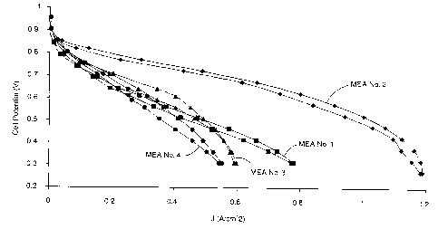
Figure 1 is a graph of polarization curves measured for a hybrid MEA of the
present invention and three comparative MEAs.
-3-
WO 00/70700 CA 02372601 2001-l0-31 PCT/iJS99/28508
Figure 2 is a graph of polarization curves measured for two hybrid MEAs of the
present invention.
Detailed Description of Preferred Embodiments
The present invention provides a hybrid membrane electrode assembly (MEA)
having an anode comprising a dense distribution of catalyst that may be borne
on small,
high-aspect ratio supports, such as nanostructured elements, and a cathode
comprising a
less dense distribution of catalyst that may be borne on lower-aspect ratio
supports such
as carbon particle-supported catalyst. Without wishing to be bound by any
theory, it is
believed that the present invention improves MEA performance by providing
excellent
water management on both electrodes.
The anode catalyst layer advantageously comprises a relatively thin layer.
Preferably the anode layer is less than 2 micrometers in thickness and more
preferably
less than 1 micrometer.
The cathode catalyst layer advantageously comprises a relatively thick layer.
Preferably the cathode layer is greater than 5 micrometer in thickness and
more
preferably greater than 10 micrometers.
The anode and cathode catalyst materials may be any effective materials.
Typical catalysts contain platinum, and may contain additional elements such
as
ruthenium. Preferably, the catalyst is a platinum containing alloy or layered
combination of platinum and a second element, as disclosed in U.S. Patent No.
5,879,828.
The distribution of catalyst material in the anode and cathode layers may be
described in terms of the electrochemical surface area/volume ratio or in
terms of the
mass/volume ratio or mass density.
The electrochemical surface arealvolume ratio may be determined by the H2
adsorption/desorption method, such as described in Canadian Patent Application
2,195,281. This method is based on the phenomena of HZ adsorption/desorption
on Pt
at the potentials immediately preceding the hydrogen evolution. It is known
that
hydrogen monolayer will adsorb on a Pt surface and exchange 220 ~C of charge
per 1
-4-
CA 02372601 2001-10-31
WO 00/70700 PCT/US99/28508
cm2 of Pt area in the process. By integration of adsorption/desorption peaks
of
hydrogen a real-to-geometrical surface area factor can be calculated.
The electrochemical surface area/volume ratio of the anode layer is preferably
greater than 200 cm2/mm3, more preferably greater than 300 cm2/mm3 and most
preferably greater than 500 cm2/mm3. The electrochemical surface area/volume
ratio of
the cathode layer is preferably less than 200 cm2/mm3 and more preferably less
than
150 cm2/mm3 and most preferably less than 100 cm2/mm3.
The mass density, or mass/volume ratio of catalyst material in each layer may
be
determined by dividing the mass of catalyst applied by the volume of the
catalyst layer.
The thickness of the layer may be determined by inspection of a membrane cross-
section by electron microscopy.
The mass density of the anode layer is preferably greater than 1.0 mg/mm3,
more preferably greater than 2.0 mg/mm3 and more preferably greater than 3.0
mg/mm3. The mass density of the cathode layer is preferably less than 1.0
mg/mm3,
more preferably less than 0.5 mg/mm3 and more preferably less than 0.3 mg/mm3.
The desired electrochemical surface area/volume ratios and mass densities may
be obtained by appropriate choice of catalyst support particles and
distribution of those
particles in the electrode layer.
The anode layer preferably comprises a thin layer of nanostructured elements,
which comprise catalyst supported on nanostructured particles. U.S. Patent No.
5,879,828, concerns MEAs having electrode layers comprising nanostructured
elements. U.S. Patent No. 5,879,827, concerns nanostructured elements bearing
nanoscopic catalyst particles which are preferred for use in the hybrid MEAs
of the
present invention.
The process for preparing the anode layer involves deposition of catalyst
material onto oriented acicular non-conductive support particles previously
arrayed on
an initial substrate, then transfer of that film of catalyst support particles
to the surface
of an ion conducting membrane (ICM). The catalyst is applied to the outer
surface of
the support particles and the catalyst support particles are localized within
a layer 2
micrometers thick or more preferably 1 micrometer thick. Pt particles are
distributed
over larger non-conductive, acicular shaped support particles located at the
surface of
-5-
CA 02372601 2001-10-31
WO 00/70700 PCT/US99/28508
the ICM. In one embodiment, the Pt catalyst particles are seen in transmission
electron
micrographs as black dots, estimated to be less than about 5 nm in size,
decorating
pieces and fragments of non-conductive support particles. The support
particles may be
embedded within the membrane or partially embedded. The support particles need
have no spatial characteristic in common other than that they are localized
within a very
thin layer, preferably less than 2 microns thick, at the surface of the ICM.
For a given
catalyst loading (in mg/cm2) the electrochemical activity of the catalyst
electrode is
directly related to the active surface area of that catalyst. That surface
area is in turn
determined by the number of catalyst particles and their sizes, since the
smaller the
particle the higher the surface area to volume ratio. For high catalyst
activities in fuel
cell electrodes, catalyst particles with dimensions in the range of 2-10 nm
are desirable.
For the purpose of illustration, if 0.02 mg/cm2 of Pt catalyst is dispersed
into
2.5 nm diameter particles, distributed into a membrane surface layer 1
micrometer
thick, then the number density of particles in this surface region would be 14
x
101~/cm3. This is an order of magnitude larger than the number density that
would be
found for similar sized catalyst particles if they were supported on typical
carbon
particles, which occupy a much larger volume, and which are typically applied
in layer
thickness of at least 10 microns.
The catalyst support of the anode layer of the MEA of the present invention
also
shows improved weight per cent loading of catalyst. The acicular support
particles can
support much higher weight percentages of catalyst while the catalyst particle
size
remains relatively small. This distinguishes commonly used carbon particles.
For
example, a common catalyst currently sold by E-tek, Inc., Natick, MA, for use
in fuel
cells is 10 to 40 wt % Pt on Vulcan XC-72 carbon black. Higher weight
percents,
beyond 80%, lead to larger catalyst particles and lower specific surface area
of the
catalyst. For example, catalyst particles composed of 80% Pt on Vulcan XC-72
carbon
black have an average particle size of 25 nm (see, e.g., E-tek 1995 Catalog).
Additional
data appear in Table I:
-6-
WO 00/70700 CA 02372601 2001-l0-31 PCT/US99/28508
Table I
Catalyst Average Pt
Particle Size
(Angstroms)
Vulcan XC-72 only --
10% Pt on Vulcan 20
XC-72
20% Pt on Vulcan 25
XC-72
30% Pt on Vulcan 32
XC-72
40% Pt on Vulcan 39
XC-72
60% Pt on Vulcan 88
XC-72
80% Pt on Vulcan 250
XC-72
Fuel Cell Grade Pt 100
Black
In one contrasting embodiment, nanostructured support particles have a mass
density of 0.005 mg/cm2 and are coated with at least 0.025 mg/cmz of platinum,
representing a catalyst wt % of 83.3. Transmission electron micrographs
demonstrate
that catalyst particle size is still on the order of 4 nm even at that 83.3%
loading.
Hence, in contrast to conventional catalyst supports, nanostructured support
particles
can support extremely high wt % loadings of catalyst without loss of the
desirable small
sized particles having a high surface area-to-volume ratio.
The use of nanostructured elements in the anode layer is one factor allowing
an
extremely high weight percent loading of catalyst, while still obtaining small
catalyst
particles having a high surface area-to-volume ratio. This is due to 1 )
nucleation of the
catalyst into small distinct particles as it is deposited on the support
particles, 2) the
density of distinct catalyst particles on the surface of each element, 3) the
acicular shape
of the nanostructured elements, and 4) the large number of elements per unit
area.
Nanostructured elements suitable for use in the present invention may comprise
metal-coated whiskers of organic pigment, most preferably C.I. PIGMENT RED 149
(perylene red). The crystalline whiskers have substantially uniform but not
identical
cross-sections, and high length-to-width ratios. The nanostructured whiskers
are coated
with materials suitable for catalysis that endow the whiskers with a fine
nanoscopic
surface structure capable of acting as multiple catalytic sites.
The cathode layer may comprise catalyst supported on carbon particles. Such
conventional supported catalysts are typically prepared by wet chemical
methods, such
CA 02372601 2001-10-31
WO 00/70700 PCT/US99/28508
as the reduction of chloroplatinic acid, and supported on carbon support
particles. This
conventional form of catalyst is dispersed with ionomeric binders, solvents
and often
polytetrafluoroethylene (PTFE) particles, to form an ink, paste or dispersion
that is
applied to either the membrane or the electrode backing material. In addition
to
mechanical support, it is generally believed in the art that the carbon
support particles
provide necessary electrical conductivity within the electrode layer.
In another variation, a catalyst metal salt is reduced in an organic solution
of a
solid polymer electrolyte to form a distribution of catalyst metal particles
in the
electrolyte without a support particle. The solid polymer electrolyte is then
cast onto an
electrode backing layer to form the catalyst electrode.
In a further variation, Pt fines are mixed directly with a solution of
solvents and
optionally polymer electrolyte and TeflonT"" and coated onto the electrode
backing layer.
However, because of limitations on how small the fines can be made and the
stability of
the dispersion, this approach results in very high, and therefore expensive,
loading of
the catalyst.
The cathode layer may also comprise nanostructured elements if they are
dispersed so as to obtain a desired catalyst distribution. For this purpose,
nanostructured elements may be dispersed in a suspension which may comprise
ionomeric binders, solvents and often polytetrafluoroethylene (PTFE)
particles, to form
an ink, paste or dispersion that is applied to either the membrane or the
electrode
backing material. Nanostructured elements may be separated from their
substrate and
suspended by any suitable method, including fluid j ets such as air, water, or
other
solvent, scraping, ultrasonic vibration, freeze fracturing, and the like.
The cathode layer may alternately combine a nanostructured catalyst layer and
a
dispersed catalyst layer if the desired catalyst distribution is obtained for
the combined
cathode layer.
It has been found that the advantages of the present invention are better
realized
with use of thinner polymer electrolyte membranes, preferably about 50
micrometers or
less (e.g., NafionT"" 112) and more preferably about 25 micrometers or less.
Preferably,
the membrane is stretched such that it is reduced in thickness prior to
incorporation in
_g_
CA 02372601 2001-10-31
WO 00/70700 - PCT/US99/28508
the MEA. In one preferred embodiment a NafionT"" 112 membrane is uniaxially or
biaxially stretched to reduce its thickness by about half.
This invention is useful in electrochemical devices such as fuel cells,
electrolyzers, batteries, or gas, vapor or liquid sensors, using membrane
electrodes
optimized for the immediate purpose.
Objects and advantages of this invention are further illustrated by the
following
examples, but the particular materials and amounts thereof recited in these
examples, as
well as other conditions and details, should not be construed to unduly limit
this
invention.
Examples
Nanostructured elements
In the following examples, the nanostructured catalyst supports were made
according to the process described in U.S. Patent No. 5,338,430, and other
patents
referenced therein. Nanostructured perylene red (PR149, American Hoechst
Corp.,
Somerset, NJ) films on polyimide substrates were made using the techniques
described
in U.S. Patent Nos. 4,812,352 and 5,039,561 by thermal evaporation and vacuum
annealing of the organic pigment C.I. Pigment Red 149, i.e., N,N'-di(3,5-
xylyl)perylene-3,4:9,10-bis(dicarboximide). After deposition and annealing,
highly
oriented crystal structures were formed with large aspect ratios, controllable
lengths of
about 0.5 to 2 micrometers, widths of about 0.03-0.05 micrometer and areal
number
density of approximately 30 whiskers per square micrometer, oriented
substantially
normal to the polyimide substrate. These microstructure catalyst supports are
nonconductive until coated with a metal catalyst and separate readily from the
polyimide substrate when pressed into an ICM. Catalyst material was coated on
the
whiskers by e-beam deposition.
Measurement of catalyst loading was done by a simple gravimetric method after
deposition. A sample of the polyimide-supported nanostructured film layer was
massed
using a digital balance accurate to about one microgram. Then the
nanostructured layer
was wiped off the polyimide substrate using a paper tissue or linen cloth, and
the
substrate was remassed. Because a preferred property of the nanostructured
catalyst
-9-
CA 02372601 2001-10-31
WO 00/70700 PCT/US99/28508
support is that it transfer easily and completely to the ion exchange
membrane, it also
was easily removed by simple wiping with a cloth. The mass per unit area of
the
catalyst support particles, without Pt, was also measured this way.
Nanostructured elements were incorporated into MEAs using a static pressing
procedure or a nip rolling procedure. The static pressing procedure consisted
of transfer
of the catalyst-coated nanostructured elements into the Nafion membrane by
pressing
under vacuum at 130 °C and a pressure of 160 MPa. The nip-rolling
procedure
consisted of transfer of the catalyst-coated nanostructured elements into the
membrane
by application of 0.75 MPa of cylinder pressure at 185 °C at web speed
of 0.3 m/min.
Catalyst densities (mg/mm3) were calculated by dividing the catalyst loading
(mg/mm2) by the average layer thickness. Average catalyst layer thicknesses
were
determined by inspection from scanning electron microscope images of layer
cross-
sections. For dispersed catalyst layers, catalyst mass was measured by a
simple
gravimetric method after ink-coating a specific area. The substrate to be
catalyzed was
weighed, the catalyst was applied and the catalyzed substrate was dried and re-
weighed.
The weight of Pt deposited was calculated from the total weight of deposit
multiplied
by the weight per cent of Pt in the non-volatile components of the ink.
Catalyst loading
was calculating by dividing catalyst mass by the area of the surface coated.
Catalyst electrochemical surface area/volume ratios (cmz/mm3) for
nanostructured electrode layers were determined using nanostructured elements
essentially equivalent to.those used in the Examples below. (The test whiskers
are
shorter than those appearing in the Examples, and therefore densities may be
greater in
the Examples.) Nanostructured samples for the experimental procedure were
prepared
on gold substrates, which were polished with 0.5 ~,m particle size alumina on
a
polishing pad with water as lubricant. Gold was chosen for its lack of
electrochemical
activity in the potential window under study, inertness and low background
currents.
Perylene red whiskers were grown on the substrates, as described above, by
evaporative
deposition of 50 nm of perylene red followed by annealing in an oven at 240-
245 °C.
These were covered with various amounts of Pt by vacuum deposition to form
working
electrodes.
-10-
WO 00/70700 CA 02372601 2001-l0-31 pCT~S99/28508
Samples were mounted in sample holder and placed in heated 3-electrode
electrochemical cell. Experimental data were collected using a PAR 263
voltammetric
analyzer, the working electrode described above, having 0.95 cmz active area,
a Pt
counter electrode, deaerated 1.0 M HZS04 as electrolyte, and under a N2
blanket.
Electrode electrochemical pretreatment involved cycling the electrode between -
0.24
V/SCE and 1.26 V/SCE at 25 mV/s for 10 cycles, starting potential 0.5 V/SCE,
followed by cycling between -0.44 V/SCE and 1.66 V/SCE at 25 mV/s for 10
cycles,
starting potential 0.5 V/SCE, followed by 10 cycles between -0.24 V/SCE and
0.5
V/SCE also at 25 mV/s with the last cycle recorded. In order to limit the
influence of
noise levels on measurement the entire electrochemical cell was enclosed in a
Faraday
cage.
The electrochemically accessible surface determination was based on the
phenomena of H2 adsorption/desorption on Pt at the potential immediately
preceding
hydrogen evolution. It is known that hydrogen will adsorb on a Pt surface and
will
exchange 220 ~.C of charge per 1 cm2 of Pt area in the process. By integration
of
adsorption/desorption peaks of hydrogen a real-to-geometrical surface area
factor can
be calculated. The region of voltammogram used for charge integration was
between -
0.2 and 0.1 V/SCE and was background corrected. The baseline, consisting
mainly of
charging currents and any impurities present in a system, was estimated based
on the
0.1 to 0.4 V/SCE potential window, where no electrochemistry is expected on Pt
in 1.0
M H2S04 electrolyte. In addition, values of charge exchanged during
voltammetric
sweep were averaged over negative and positive going scans.
For the nanostructured catalyst, the value of electrochemical surface area
thus
obtained for Pt catalyst loadings between 13 ~.g/cm2 and 650 ~,g/cm2 was 8.2
m2/g. For
loading of 0.2 mg/cm2 of Pt, this corresponds to 16.4 cm2 of electrochemically
active
catalyst surface per 1 cmZ of planar electrode area. Since the thickness of
nanostructured catalyst of 0.2 mg/cm2 of Pt as deposited onto membrane is
between 0.2
and 0.5 ~.m (see, e.g., US Patent 5,879,828), the electrochemical surface area
to volume
ratio of this catalyst is between 300-800 cm2/mm3. The surface area may be
somewhat
higher in the examples below because longer nanostructured elements were used.
-11-
CA 02372601 2001-10-31
WO 00/70700 PCT/US99/28508
Dispersed Catalyst Layers
The dispersed catalyst layers used in the following examples were trilayers
made by coating a catalyst composition layer on a 0.28 cm (0.011 ") thick
bilayer
electrode backing material, comprised of a Toray paper electrode backing layer
coated
with a carbon/teflon layer (International Fuel Cells, South Windsor,
Connecticut). A
comparable coated Toray in the practice of the present invention was shown to
be
Model # 39-GDE-501 available from Johnson Mathey (Reading, Berkshire,
England).
The catalyst layer was applied onto the coated Toray as a dispersion in water
and
isopropanol. The catalyst composition layer contained 39% by weight of 30%Pt/C
(E-
tek, Inc., Natick, MA), 41 % of glycerin and 20% of NafionT"" 1000. The
thickness of
the catalyst layer ranged from 10 pm to 30 pm.
Other dispersed catalyst layers used in the following examples were made by
coating a catalyst layer on a 430 pm thick ELATT~~ gas diffusion electrode
available
from E-Tek, Natick, MA. Catalyzed carbon used for ink making was 30% Pt/C
obtained from E-Tek, Natick, MA. Catalyst composition was 670 mg of 5% (w/o)
NafionT"" 1000 solution in lower alcohols (DuPont Chemicals, Wilmington, DE),
67 mg
of 30% Pt/C and 75 mg of glycerin. Catalyst was applied by simple brushing
method in
such a way that resulted in coverage between 183 and 266 pg of Pt per 1 cm2 of
planar
area of the electrode.
For dispersed catalyst, the catalyst electrochemical surface area per unit
volume
was calculated using surface area and thickness data reported by the
manufacture in
Ralph et al, Low Cost Electrodes for Proton Exchange Membrane Fuel Cells, J.
Electrochem. Soc. Vol. 144, No. 11, (Nov. 1997) at Table I, page 3848 and at
page
3851.
ICM
The ion conducting membranes used were perfluorinated sulfonic acid
materials, specifically, NafionTM 112 membranes (DuPont Chemicals, Wilmington,
DE,
available from ElectroChem, Inc., Woburn, MA, and Aldrich Chemical Co., Inc.,
Milwaukee, WI). Before use. the NafionT"" membrane was pretreated by
sequentially
immersing into a) boiling water for one hour, b) boiling 3% H202 for one hour,
c)
boiling ultra pure H20 for 1 hour, d) boiling 0.5 M HZS04 for one hour, e)
boiling ultra
-12-
WO 00/70700 CA 02372601 2001-10-31
PCT/US99/28508
pure DI HZO for one hour. The membrane was then stored in ultrapure DI water
until
use. Prior to forming an MEA the membrane was dried by laying it between
several
layers of clean linen cloth at 30° C for 10-20 minutes. The membranes
were then
stretched with a Film Stretcher (T.M. Long Co., Inc.; Somerville, NJ) equipped
with a 4
X 4 stretching head. The thickness of the membranes was thereby reduced from
50
micrometers to about 25 micrometers.
Example 1
Four MEAs were constructed having the electrode composition noted in Table
II. MEAs No. 1, 3 and 4 are comparative and MEA No. 2 exemplifies the present
invention.
Table II
MEA No. Anode Cathode
1 C Nanostructured Nanostructured
2 Nanostructured Dispersed
3C Dispersed Nanostructured
4C Dispersed Dispersed
MEA's having nanostructured elements on both electrode surfaces were
prepared as follows: A three-layer MEA with 5 cm2 of active area was prepared
by a
static pressing method. Two 5 cm2 square pieces of ~1.5 qm long nanostructured
elements on a polyimide substrate - one for the anode, one for the cathode -
were placed
on either side of the center of a 7.6 cm x 7.6 cm NafionT"" membrane prepared
as
indicated above. A 50 micrometer thick, 7.6 cm x 7.6 cm sheet of polyimide was
placed on each side of the catalyst coated substrate/Nafion/catalyst coated
substrate
sandwich. This assembly was then placed between two steel shim plates and
pressed
under a low grade vacuum at 130° C and a pressure of 160 MPa using a
Carver lab
press (Carver Inc., Wabash, IN). A low grade vacuum (less than about 2 Torr)
was
applied to partially remove air from the stack just prior to applying the
maximum
pressure. The original 5 cmz polyimide substrates were then peeled away
leaving the
catalyst attached to the surface of the Nafion membrane. For preparation of a
five-layer
-13-
CA 02372601 2001-10-31
WO 00/70700 PCT/L1S99/28508
MEA, the above three-layer MEA was covered with 0.28 cm (0.011 ") thick Toray
type
GDE electrode backing material. The Toray type GDE electrode backing material
was
uniformly brushed with glycerin before attachment. The assembly was then
placed
between two 200 micrometers thick TeflonTM coated fiberglass gaskets (The
Furon Co.,
CHR Division, New Haven, CT) each having a in a 5 cm2 square hole cut to match
the
catalyst area. A 50 micrometer thick, 7.6 cm x 7.6 cm sheet of polyimide was
then
placed on each side. This assembly was then placed between two steel shim
plates and
pressed under a low grade vacuum at 130° C and a pressure of 2.8 MPa
using a Carver
lab press (Carver Inc., Wabash, IN). A low grade vacuum (less than about 2
Torr) was
applied to partially remove air from the stack just prior to applying the
maximum
pressure. The polyimide sheets were then peeled away leaving the five-layer
MEA
having nanostructured elements on both electrode surfaces.
MEAs having nanostructured elements on one electrode surface and dispersed
catalyst on the second surface were prepared as follows: For preparation of a
two-layer
MEA with 5 cm2 of active area by a static pressing method, one 5 cm2 square
piece of
the nanostructured elements on a polyimide substrate was placed on one side of
the
center of a 7.6 cm x 7.6 cm stretched Nafion membrane. A 50 micrometer thick,
7.6
cm x 7.6 cm sheet of polyimide was placed on each side of the catalyst coated
substrate/Nafion bilayer. This assembly was then placed between two steel shim
plates
and pressed under a low grade vacuum at 130° C and a pressure of 160
MPa using a
Carver lab press (Carver Inc., Wabash, IN). A low grade vacuum (less than
about 2
Torr) was applied to partially remove air from the stack just prior to
applying the
maximum pressure. The original S cm' polyimide substrate was then peeled away
leaving the catalyst attached to one side (anode side) of the Nafion membrane.
This
two-layer MEA was covered with 0.28 cm (0.011 ") thick Toray type GDE
electrode
backing material (JM). The assembly was then placed between two 200
micrometers
thick TeflonTM coated fiberglass gaskets (The Furon Co., CHR Division, New
Haven,
CT) each having a in a 5 cm2 square hole cut to match the catalyst area. The
Toray type
GDE electrode backing material on anode side was wetted by glycerin, and
attached to
the nanostructured catalyst surface of the two layer MEA. The Toray type GDE
electrode backing material on the cathode side was coated by brush with an ink
-14-
CA 02372601 2001-10-31
WO 00/70700 PCT/US99/28508
composed of 8 wt% of 30% Pt/C (E-tek, Inc., Natick, MA), 4 wt% of NafionT""
1000, 9
wt% of glycerin, 79 wt% water/isopropanol mixture to a thickness of 10 micron
and Pt
loading of 0.3 mg/cm2, dried at 60 °C under vacuum for 10 mins, then
attached to the
membrane side. A 50 micrometer thick, 7.6 cm x 7.6 cm sheet of polyimide was
placed
on each side. This assembly was then placed between two steel shim plates and
pressed
under a low grade vacuum at 130° C and a pressure of 2.8 MPa using a
Carver lab press
(Carver Inc., Wabash, IN). A low grade vacuum (less than about 2 Torr) was
applied to
partially remove air from the stack just prior to applying the maximum
pressure. The
polyimide sheets were then peeled away leaving the five-layer MEA with
nanostructured elements on one electrode surface and dispersed catalyst on the
second
surface.
MEAs having dispersed catalyst on both surfaces were prepared as follows:
Toray type GDE electrode backing material (275 micrometer) were coated by
brush
with an ink composed of 8 wt% of 30% Pt/C (E-tek, Inc., Natick, MA), 4 wt% of
NafionT"" 1000, 9 wt% of glycerin, 79 wt% water/isopropanol mixture to a
thickness of
10 microns and Pt loading of 0.3 mg/cm2, then dried at 60 °C under
vacuum for 10
minutes to form a catalyst-coated GDE. The assembly was then placed between
two
200 micrometers thick TeflonTM coated fiberglass gaskets (The Furon Co., CHR
Division, New Haven, CT) each having a in a 5 cm2 square hole cut to match the
catalyst area. A 50 micrometer thick, 7.6 cm x 7.6 cm sheet of polyimide was
placed
on each side. This assembly was then placed between two steel shim plates and
pressed
under a low grade vacuum at 130° C and a pressure of 2.8 MPa using a
Carver lab press
(Carver Inc., Wabash, IN). A low grade vacuum (less than about 2 Torr) was
applied to
partially remove air from the stack just prior to applying the maximum
pressure. The
polyimide sheets were then removed leaving the five-layer MEA with dispersed
catalyst
on both electrode surfaces.
Values of catalyst density (mg/mm3), catalyst electrochemical surface
area/volume ratio (cm2/mm3) and catalyst layer thickness for the
nanostructured and
dispersed electrode layers used in the present examples are reported in Table
III:
-15-
CA 02372601 2001-10-31
WO 00/70700 PCT/US99/28508
Table III
Catalyst Pt LoadingCatalyst Catalyst Catalyst
Lager
m /cm2 density electrochemicallayer
m /mm3 surface area/volumethickness
ratio (cm2/mm3)m
Nanostructured0.20 4.0 320 0.5
Dispersed 0.30 0.3 180 10
In the Examples herein, five-layer MEA's were mounted in a test cell station
(Fuel Cell Technologies, Inc., Albuquerque, NM). The test station includes a
variable
electronic load with separate anode and cathode gas handling systems to
control gas
flow, pressure and humidity. The electronic load and gas flow are computer
controlled.
Fuel cell polarization curves were obtained under the following test
parameters:
electrode area, 5 cm2; cell temperature, 65° C, anode gas pressure 0.1
MPa; anode gas
flow rate, 100 standard cc/min; anode humidification temperature, 65°
C; cathode gas
pressure 0.1 MPa; cathode flow rate, 300 standard cc/min; cathode
humidification
temperature, 65° C. Humidification of the cathode gas streams was
provided by passing
the gas through spurge bottles maintained at the stated temperatures.
Humidification of
the anode gas streams was provided by pumping 0.05 cc/min water via a HPLC
pump
through a heated pipe at the stated temperatures. Each fuel cell was brought
to
operating conditions at 65° C under hydrogen and air flows. Test
protocols were
initiated after 24 hours of operation and the following variables were
measured: anode
pressure, anode flow, cathode pressure, cathode flow, and cell temperature.
Figure 1 shows the polarization curves obtained for these four MEAs. The
curves demonstrate significantly higher performance for MEA No. 2, the hybrid
MEA
having a nanostructured anode and dispersed cathode. More specifically, MEA
No. 2
achieves higher power output over all portions of the current density/voltage
curve.
Example 2
Two MEAs were constructed which exemplify the present invention. MEA No.
5 had a nanostructured anode and a dispersed cathode. MEA No. 6 had a
nanostructured anode and a gradient cathode, which is a nanostructured cathode
-16-
WO 00/70700 CA 02372601 2001-10-31 pCT~S99/28508
overlayed with a dispersed cathode layer to form a composite cathode layer
having a
density gradient.
The MEAs were prepared as follows:
The dispersed catalyst layers used in the following examples were made by
coating a catalyst layer on a 430 qm thick ELATT"" gas diffusion electrode
available
from E-Tek, Natick, MA. The ink was composed of 8 wt% of 30% Pt/C (E-tek,
Inc.,
Natick, MA), 4 wt% of NafionT"~ 1000, 9 wt% of glycerin, 79 wt%
water/isopropanol
mixture. Ink was applied by simple brushing method that resulted in coverage
between
183 and 266 q.g of Pt per 1 cm2 of planar area of the electrode.
Nanostructured elements were incorporated into each MEA using a nip-rolling
procedure which consisted of transfer of the catalyst-coated nanostructured
elements
into the stretched Nafion 112 membrane. The nip-rollers used were 7.5 cm
diameter
cylinders under 0.75 MPa of pressure. The rollers were heated to 185
°C. The web
speed was 0.3 m/min. One or two-sided transfer was used, depending on the MEA.
An MEA having nanostructured elements on one side only was prepared as
follows: A two-layer MEA with 50 cm2 of active area was prepared by a nip-
rolling
method. One 50 cm2 square piece of the nanostructured elements on a polyimide
substrate for the anode was placed on one side of the center of a 10 cm x 10
cm
NafionT"" membrane prepared as indicated above. A 50 micrometer thick, 10 cm x
10
cm sheet of polyimide was placed on each side of the catalyst coated
substrate/Nafion
sandwich. This assembly was then placed between two larger pieces of polyimide
and
run through the rollers. The original 50 cm2 polyimide substrate was then
peeled away
leaving the catalyst attached to one surface of the Nafion membrane.
For preparation of a five-layer MEA, the above two-layer MEA was covered on
the catalyzed side with 430 q.m ELAT electrode backing material. The ELAT
electrode
backing material was wetted by Nafion 1000/glycerin solution (prepared by
mixing
equal volumes of 5% Nafion 1000 solution and glycerin) before attachment. The
resulting Nafion loading of a diffuser was 31.2 ~g/cm2. The non-catalyzed side
of the
two-layer MEA was placed against 7.1 cm by 7.1 cm piece of catalyzed ELAT
having
183 ~.g of Pt per 1 cm2 of planar area of the electrode. The assembly was then
placed
between two 200 micrometers thick TeflonTM coated fiberglass gaskets (The
Furon Co.,
-17-
W~ 00/70700 CA 02372601 2001-10-31
PCT/US99/28508
CHR Division, New Haven, CT) each having a in a 5 cmz square hole cut to match
the
catalyst area. A 50 ~m thick, 10 cm x 10 cm sheet of polyimide was then placed
on
each side. This assembly was then placed between two steel shim plates and
pressed
using a Carver lab press (Carver Inc., Wabash, IN) at 135 °C and a
pressure of 2 MPa
for 600s followed by 5 MPa for 30 seconds. The polyimide sheets were then
removed
leaving the five-layer MEA with nanostructured elements on one electrode
surface and
dispersed catalyst on the second surface.
MEAs having nanostructured elements on both electrode surfaces were prepared
as follows: A three-layer MEA with 50 cm2 of active area was prepared by a nip-
rolling
method. Two 50 cm2 square pieces of the nanostructured elements on a polyimide
substrate - one for the anode, one for the cathode - were placed on either
side of the
center of a 10 cm x 10 cm NafionT"" membrane prepared as indicated above. A 50
micrometer thick, 10 cm x 10 cm sheet of polyimide was placed on each side of
the
catalyst coated substrate/Nafion/catalyst coated substrate sandwich. This
assembly was
then placed between two larger pieces of polyimide and run through the
rollers. The
original 50 cm2 polyimide substrates were then peeled away leaving the
catalyst
attached to the surface of the Nafion membrane.
For preparation of a five-layer gradient MEA (MEA No. 6), the anodic
catalyzed side of the above three-layer MEA was covered with 50 cm2 430 ~m
thick
piece of ELAT electrode backing material. The ELAT electrode backing material
was
wetted by brushing with Nafion 1000/glycerin solution (prepared by mixing
equal
volumes of 5% Nafion 1000 solution and glycerin) before attachment. The
resulting
Nafion coating weight was 28.9 p.g/cm2. The catalyzed cathode side of the
three-layer
MEA was placed against a 7.1 cm by 7.1 cm piece of ELAT catalyzed with 266 ~,g
of
Pt per 1 cm2 of planar area of the electrode. The assembly was then placed
between two
200 micrometers thick TeflonTM coated fiberglass gaskets (The Furon Co., CHR
Division, New Haven, CT) each having a in a 5 cm2 square hole cut to match the
catalyst area. A 50 ~m thick, 10 cm x 10 cm sheet of polyimide was then placed
on
each side. This assembly was then placed between two steel shim plates and
pressed
using a Carver lab press (Carver Inc., Wabash, IN) at 135 °C and a
pressure of 2 MPa
for 600s followed by 5 MPa for 30 seconds. The polyimide sheets were then
peeled
-18-
WO 00/70700 CA 02372601 2001-l0-31 pCT~S99/28508
away leaving the five-layer MEA with nanostructured elements on one electrode
surface and both nanostructured and dispersed catalyst on the second surface.
For testing, the above five-layer MEAs were mounted in single cells and
connected to a fuel cell test station (Fuel Cell Technologies, Inc.,
Albuquerque, NM).
The test station includes a variable electronic load with separate anode and
cathode gas
handling systems to control gas flow, pressure and humidity. The electronic
load and
gas flows are computer controlled.
Fuel cell polarization curves were obtained under the following test
parameters:
electrode area, 50 cm2; cell temperature, 75° C, reactants H2/02, anode
gas pressure 0.1
MPa; anode gas flow rate, 800 standard cm3/min; anode water delivery between
0.7 and
1.0 mL/min; cathode gas pressure 0.1 MPa; cathode flow rate, 400 standard
cm3/min;
cathode water delivery 0.18 mL/min. Steam injectors provided humidification of
the
gas streams.
Figure 2 shows the polarization curves obtained for these two MEAs. The
curves demonstrate somewhat higher performance for MEA No. 6, the hybrid MEA
having a nanostructured anode and gradient cathode.
Various modifications and alterations of this invention will become apparent
to
those skilled in the art without departing from the scope and principles of
this
invention, and it should be understood that this invention is not to be unduly
limited to
the illustrative embodiments set forth hereinabove.
-19-