Note: Descriptions are shown in the official language in which they were submitted.
CA 02372799 2001-10-31
WO 01/61856 PCT/USO1/04783
SYSTEM AND METHOD FOR PROGRAMMING OSCILLATORS
FIELD OF THE INVENTION
The present invention relates to the field of programmable oscillators, and
more
particularly to systems and methods including high accuracy EPROM programmable
phase
locked loop oscillators.
BACKGROUND OF THE INVENTION
The CY2037 from Cypress Semiconductor Corporation (San Jose, CA), is an
EPROM-programmable (electrically programmable read only memory), high-accuracy
and
resolution, PLL-based (phase-locked loop) digitally controlled crystal
oscillator (DCXO).
The device has a low fitter specification, e.g., < ~100ps (pk-pk) at 5V and
f>33 MHz and <
~125ps (pk-pk) at 3.3V and f>33 MHz. The device is available die form, i.e.,
without
packaging, and attaches directly to a 10-30 MHz crystal. The oscillator device
may be
packaged into various through-hole or surface mount packages. A block diagram
of this
circuit is shown in Fig. 1A.
Traditionally, an oscillator crystal is calibrated in an operation termed the
"final
plate", from an initial accuracy of within 2,000-3,000 ppm from the nominal
frequency
desired to within 10-25 ppm (typical) from the nominal desired frequency. This
is a
significant mechanical step, and constitutes the final calibration of the
oscillator after it is
mounted in a module. The final plate involves selectively depositing a film or
plating of
metal on a prepared pre-plate portion of the surface of the crystal, to
mechanically alter the
resonant frequency of the crystal. This process is typically manually
assisted, requiring a
skilled technician to carefully apply the plating to adjust the operating
frequency of the
crystal. Not only the thickness, but also the placement of the plating is
critical; if it is not
exactly concentric over the pre-plate region, phase noise and fitter are
increased. In fact, as a
rule, phase noise and fitter increase after the final plate. The final plate
process also results in
loss of yield. For example, there is a probability of plating adhesion
failure. Further, the
final plate process is performed with the crystal exposed, and thus more
sensitive to
environmental influences. After the crystal is tuned by the final plate, the
crystal is sealed.
Thus, the final plate process is expensive, labor consuming, reduces crystal
quality, and
potentially induces defects.
CA 02372799 2001-10-31
WO 01/61856 PCT/USO1/04783
-2-
Precision crystal oscillators (PXO) such as the Micro Analog Systems (Espoo,
Finland) MAS9271 and MAS1173, which include a digitally controlled capacitive
tuning
network for trimming a crystal frequency, are typically calibrated and
operated independently
of a digital frequency synthesizer. Thus, using a PXO, a crystal is tuned to a
desired
frequency, to within a small tolerance. This may include a final plate
process. The digital
frequency synthesizer is then programmed using the nominal multiply and divide
values to
achieve the desired output frequency.
In principle, the oscillator devices can be stocked as blank parts and custom
frequencies programmed in-package at the last stage before shipping from an
oscillator
manufacturer. This would enable fast-turn manufacture of custom and standard
crystal
oscillators without the need for dedicated, expensive crystals or inventory of
customized
assemblies. In this case, the oscillators are not field programmable, and an
integrator of
oscillators into products must still specifically order a particular
oscillator at a predefined
frequency, and must still await the customization by the oscillator
manufacturer and incur
potential set-up charges, which may be significant for small orders, as well
as the added cycle
time of days or weeks.
The CY2037 contains an on-chip oscillator and a separate oscillator tuning
circuit for
fine-tuning of the output frequency. The crystal capacitive load can be
selectively adjusted by
programming a set of seven EPROM bits. This feature is typically used to
compensate for
crystal variations or to obtain a more accurate synthesized frequency.
The typical use of a programmable oscillator starts with an oscillator crystal
trimmed
to a nominal value. Then, the oscillator circuit is permanently programmed (in
EPROM)
with the multiply and divide ratios. Finally, at least in the case of the
CY2037, the operating
frequency of the crystal is tuned with the tuning bits to achieve a desired
maximum error.
The CY2037 PLL die has a very high resolution. It has a 12-bit feedback
counter
multiplier and a 10-bit reference counter divider. This enables the synthesis
of highly
accurate and stable output clock frequencies with low error, for example zero
or low parts per
million (ppm). The clock can be further modified by eight output divider
options of 1, 2, 4,
8, 16, 32, 64 and 128. The divider input can be selected as either the PLL or
crystal oscillator
output, providing a total of sixteen separate output options. The output is
selectable between
TTL and CMOS duty cycle levels.
CA 02372799 2001-10-31
WO 01/61856 PCT/USO1/04783
-3-
The nominal output frequency of the PLL is determined by the following
formula:
Fp~~ = 2 x (P + 5)/(Q + 2) x FREE
where P is the feedback counter value and Q is the reference counter value. P
and Q
are EPROM programmable values.
One version of the CY2037 contains a special tuning circuit to fine-tune the
output
frequency of the device. The tuning circuit consists of an array of eleven
logarithmically
sized load capacitors on both sides of the oscillator drive inverter. The
capacitor load values
are EPROM programmable with seven Osc Tune bits, and can be increased in small
increments. As the capacitor load is increased the circuit is fine-tuned to a
lower frequency.
The capacitor load values vary from 0.17 pF to 8 pF for an approximate 100:1
total control
ratio.
The CY2037 uses EPROM programming with a simple 2-wire, 4-pin interface that
includes VSS and VDD. Clock outputs can be generated up to 250 MHz. According
to the
design, the entire configuration of the EPROM can be reprogrammed one time,
allowing
programmed inventory to be altered or reused. The CY2037 includes a 44 bit by
2 row
EPROM block, which holds all of the configuration information. The programming
word
contains the data from the EPROM and a row select (RowSel) bit, which
determines the row
being accessed during normal operation. Cypress advises that the bit should
match in both
rows, and therefore, when row 0 is programmed, row 1 is otherwise left
unprogrammed, with
the RowSel bit row 0 programmed to 0. When row 1 is programmed, the RowSel bit
of row
0 is programmed to 1, a permissible overwrite.
The CY2037 contains a shadow register in addition to the EPROM register, which
is
optionally disabled. The shadow register is an exact copy of the EPROM
register and is the
default register when the Valid bit is not set. It is useful when the
prototype or production
environment calls for measuring and adjusting the CLKOUT frequency multiple
times.
Multiple adjustments can be performed with the shadow register. Once the
desired frequency
is achieved, the EPROM register is permanently programmed.
Accordingly, the following essential features of the CY2037 are controlled
based on
data stored in the EPROM: Feedback counter value (P); Reference counter value
(Q); Output
divider selection; Oscillator Tuning (load capacitance values); Duty cycle
levels (TTL or
CA 02372799 2001-10-31
WO 01/61856 PCT/USO1/04783
-4-
CMOS); Power management mode (OE or PWR DWN); Power management timing
(synchronous or asynchronous); and Output Source Frequency (PLL or Crystal).
A PLL-based frequency synthesizer uses a reference input to generate output
clocks.
The reference can be provided by a quartz crystal or an external clock source.
The accuracy
and stability of the output clocks in a PLL-based frequency synthesizer are
directly
proportional to those of the reference. Thus, it is important to provide a
stable, accurate, and
appropriate reference input.
Jitter is an effect caused by an irregularity in the crystal oscillation
and/or logic
transitions of the circuit electronics. This can be caused by rapid changes in
power supply
voltage, logic transition voltage, stochastic processes, radio frequency
interferences, or the
like.
Figure 1 shows the block diagram of a CY2037 PLL-based frequency synthesizer.
The reference input to the PLL comes from an on-chip crystal oscillator.
Figure 2 shows the
circuitry of the on-chip crystal oscillator (a.k.a. Pierce oscillator), which
is formed by
components R, G, Ci and Co, where G is a linear inverter. For this circuit to
produce an
electrical clock, a quartz crystal needs to be connected between the XTALIN
and XTALOUT
pms.
The equivalent circuit of a Quartz crystal is shown in Figure 3. CD is the
shunt or static
capacitance of the crystal. R1 is the motional resistance, L1 is the motional
inductance, and C,
is the motional capacitance of the crystal. R~, L1 and C1 are determined by
the mechanical
properties of the crystal (they are in the motional arm of the crystal and
their circuit effects
only exist when the crystal is oscillating). The effective reactance curve of
the crystal is
shown in Figure 4. Thus, it is seen that slight variations in the fabrication
of the quartz
crystal will alter the nominal output frequency.
When connected as a feedback element in a oscillator circuit that has a
0° phase shift,
the crystal oscillates at the series resonating frequency (f s ) given by Eq.
1:
fS = 1/(2n~(L~C1)) Eq. 1
A Pierce oscillator has a 180° phase shift on the amplifier and needs
another 180°
phase shift from the feedback element. The feedback element in this case is a
crystal along
with a capacitive load, and the frequency of oscillation of the crystal (and
oscillator circuit) is
in the "area of parallel resonance". The actual value of the crystal
oscillator parallel
CA 02372799 2001-10-31
WO 01/61856 PCT/USO1/04783
-5-
resonating frequency is dependent on the capacitive loading seen by the
crystal and is given
by Eq. 2:
f~, = fs (1 + C~/2(Co + C~) Eq. 2
where C~ = Capacitive loading seen by the crystal.
For example, a parallel resonant crystal tuned to a particular C,oad will
oscillate at a
predetermined frequency when it is placed in a Pierce oscillator (parallel
oscillator) circuit
which offers a capacitive loading C~ = C,o~d. If the capacitive loading seen
by the crystal in
the Pierce oscillator circuit were different from the rated Goad, the change
in frequency from
the rated frequency is given by Eq. 3:
(f~ (raced) - fP (actual))/fp(rated) = C~/2((1/(Cp + CL) - 1/(C0 + C~)) Eq. 3
where:
f~ (rated)= frequency rating of crystal
fP (actual)= actual frequency of oscillation in oscillator circuit
Cload = Capacitive loading rating of crystal
C~ = Capacitive loading seen by crystal in oscillator circuit.
Thus, a trim capacitor network would be expected to tune the circuit for
variations in
the crystal, allowing fine calibration of the operating frequency. This effect
is analytic, and
therefore the alteration in operating frequency due to a change in capacitance
may be
predicted with accuracy.
Typically, the selected EPROM register of the CY2037 device is programmed with
appropriate multiply (P) and divide (Q) ratios, to achieve a desired output
frequency,
typically slightly above the desired final frequency. The controller
calculates the multiply
and divide ratios based on the output of the frequency counter and an
algorithm therein,
known in the art. After the P and Q are programmed into the device, the output
of the
oscillator is measured over a number of conditions of tuning, for example
testing the effect on
the output for each of the tuning bits. The controller then determines an
optimal set of tuning
bits and these are programmed into the EPROM. Thus, the DCXO is normally first
programmed based on a nominal oscillator frequency, and the oscillator
frequency then
adjusted by trimming to achieve the desired output.
Oscillators will often have an intrinsic sensitivity to temperature. Thus, the
output
frequency will vary from a nominal value with changes in operating
temperature. It is known
CA 02372799 2001-10-31
WO 01/61856 PCT/USO1/04783
-6-
to compensate for these changes using a so-called TCXO, or temperature
compensated
crystal oscillator. The temperature compensation network may be analog or
digital. Often, it
is desired to provide a crystal controlled oscillator with a stable frequency,
which is
controllable by an external voltage. This is called a voltage controlled
crystal oscillator, or
VCXO. For example, high precision phase locked loops, and radio frequency
transceivers
may use these devices. Many TCXO devices also provide VCXO functionality, and
are
called voltage controlled, temperature compensated crystal oscillators
(VCTCXO).
Essentially, modern TCXO and VCXO devices operate by altering a capacitive
loading on the oscillator crystal in dependence on a sensed voltage. This is
typically
performed using a varactor (a diode whose capacitance varies with reverse-bias
voltage),
which responds to an analog control voltage. This provides a stepless analog
control, in
contrast to the use of switched capacitor networks used to trim the capacitive
load.
Micro Analog Systems (Espoo, Finland, www.mas-oy.com) produces a voltage
controlled, temperature compensated crystal oscillator (VCTCXO) circuit,
MAS1175, a block
diagram of which is shown in Fig. 8, which provides a three point temperature
compensation,
a serial bus for programming and trim, EPROM storage of parameters, and analog
compensation. Thus, a digital capacitive trimming network and analog
capacitive control
network are both provided. The circuit requires an external crystal and
varactor.
CA 02372799 2001-10-31
WO 01/61856 PCT/USO1/04783
_7_
SUMMARY AND OBJECTS OF THE INVENTION
The present invention provides a number of enhancements to digitally
controlled
oscillator systems. According to a first embodiment, the present invention
provides a system
and method for field programming an EPROM programmable oscillator device,
using a
relatively simple programmer device and a terminal or personal computer.
According to another aspect of the invention, the final plate process for
tuning the
crystal is eliminated, and the processes of electronically tuning the crystal
and selecting
operating parameters for a digital frequency synthesizer are consolidated in a
single process.
Thus, by treating the tuning registers for the crystal oscillator as an
integral part of the
frequency control of the output, a production step is eliminated, greater
flexibility in selecting
operating parameters is obtained, and quality is improved.
The EPROM programmable oscillator device preferably includes electronically
controllable tuning of crystal frequency as well as high precision frequency
synthesis.
According to the present invention, these two attributes are combined to
dispense with the
necessity of the final plate, and, for example, to thereby increase output
quality (reduced
phase noise and jittery, increase product quality (reduce probability of
environmental
contamination of crystal or delamination of plating), decrease costs, decrease
skilled manual
labor required, decrease manufacturing cycle time (and allow decentralization
of final
production steps with field programmability), allow standardization of
completely
manufactured oscillators, and/or increase manufacturing yield.
The present invention also provides a further enhancement for reducing
oscillator
fitter. In testing an oscillator designed using a quartz crystal and CY2037
packaged in an
industry standard 5 x 7 mm metal package with ceramic substrate, over a
frequency range
(output) of 10-120 MHz, fitter ranged from 95-220 ps (bimodal
distribution)(25,000
samples). However, when an internal power supply bypass capacitor of between
10 nF and
100 nF was placed inside the package, fitter was reduced to between 55-120 ps
(Gaussian-
type distribution) (25,000 samples). Typically, bypass capacitors are placed
on the
component circuit board, not within the oscillator package, therefore, this
significant
advantage was surprising. It is likely that this reduction in fitter results
from the inductance
of the package leads. By providing the bypass capacitor within the oscillator
package, the
circuit is better isolated from the effects of this inductance. According to
the present
CA 02372799 2001-10-31
WO 01/61856 PCT/USO1/04783
_g_
invention, it is also possible to provide the internal bypass capacitor in
conjunction with
tuning the inductance of the power supply lines leading to the circuit, to
form a filter, to
further reduce fitter.
Advantages of field programmability include reduced prototype and
manufacturing
cycle time, and allowing oscillator users to inventory unprogrammed parts,.
which are
programmed to specification as needed.
Oscillators according to the present invention provide programming capability
of
greater than 6 significant digits of accuracy, over a frequency range of 1 to
250 MHz,
covering both the commercial and industrial temperature ranges. Temperature
compensated
versions as well as voltage controlled versions, are also within the scope of
the invention.
In order to provide a temperature-compensated high-resolution digitally
controlled
oscillator, one embodiment provides a VCTCXO circuit output as an input
(replacing the
crystal at X~) for the CY2037 DCXO. The internal trim capacitors of the CY2037
are not
employed, and versions of the device where these are unavailable may be
employed. In
programming this system, the VCTCXO control parameters are first calculated,
for example
with compensation determined at three different temperatures. The control
parameters may
be programmed, to test the nominal (untrimmed) output, or the predicted output
may be used,
but the trimming network parameters remain unprogrammed. The various P, Q and
divider
values of the DCXO and the capacitive trimming network parameters may together
be
calculated and then programmed.
Likewise, the present invention also provides an integrated (e.g., single
integrated
circuit) high resolution DCVCTCXO. In this case, the internal capacitive
trimming may
coexist with the temperature compensation, voltage control and logic control
circuitry.
Advantageously, the control electronics for all functions use a single serial
interface and set
of non-volatile control registers.
The process for programming the DCXO (CY2037) essentially determines the free
crystal oscillator operating frequency, for example over a range of available
tuning values,
and then calculates the optimal P, Q, divider select and tuning value to
achieve the desired
oscillator operating frequency with acceptable error (ppm), with the lowest Q
value.
Therefore, in contrast to typical prior art methods, the crystal tuning is
performed
simultaneously with selection of oscillator parameters P, Q, and divider
select, rather than
CA 02372799 2001-10-31
WO 01/61856 PCT/USO1/04783
-9-
beforehand. This results in greater flexibility for optimizing the various
parameters. In this
process, therefore, the P, Q and divider select parameters may vary between
oscillators that
meet the same output frequency specification, due to differences in the
crystal and tuning
parameters.
Therefore, one aspect of the invention provides a high precision oscillator
system that
does not require a finely tuned oscillator crystal. Another aspect of the
invention provides
that the oscillator is programmed with both fine-tuning of crystal operating
frequency and
output frequency translation in a consolidated operation. A further aspect of
the invention
provides a programming device for a programmable oscillator, which selects
optimum crystal
frequency tuning and frequency synthesis in a single operation.
Therefore, the present invention provides a human user interface system and
method
that provides an interface with a programmable oscillator device, for
programming thereof,
which meet all or some of the objects identified herein.
Initially, the nominal frequency of the crystal is measured using a frequency
counter.
This frequency is preferably measured with the programmable oscillator in an
unprogrammed
state, such that the crystal frequency itself is measured. Preferably, the
tuning sensitivity of
the system is also measured, by testing the crystal output over a range of
available tuning
values. Typically, a small number of measured values are required, for
example, eight
measurements within a seven-bit tuning system. While the output frequency for
each bit
combination could also be measured, e.g., all 128 values for a seven bit
range, but this is not
necessary, as the tuning effects may generally be accurately predicted based
on a sparse
sampling of this range, preferably testing the sensitivity of each bit, but
not necessarily
separately. The tuning effects of bits, which represent added capacitance on
the crystal, and
which lower its operating frequency, are typically non-linear; therefore, a
lower order bit will
have a reduced effect on output, e.g., result in a lower ppm change, when the
total
capacitance load on the crystal is higher.
The sensitivity of the tuning bits is tested using a temporary programming
technique,
e.g., a shadow register. By altering the contents of the shadow register, the
capacitive effect
of the tuning capacitor loading on the crystal is determined without
permanently modifying
the oscillator. Thus, the tuning sensitivity may be determined before
programming the
CA 02372799 2001-10-31
WO 01/61856 PCT/USO1/04783
-10-
oscillator, which in the unprogrammed state (e.g., CY2037) outputs the crystal
reference
without regard for the P, Q and divider select.
In the case of a DCVCTCXO, (e.g., combination MAS1175 and CY2037), the
temperature compensation network (e.g., MAS1175) may also be maintained in an
unprogrammed state until the coefficients for the digital PLL divider network
(CY2037) are
calculated. This allows, in the event of an undersirable set of P, Q, and
divider ratio, a
selection of an alternate set of temperature compensation parameters (than
those provided by
the normal algorithm) to be programmed. Thus, in the same way that the trim
capacitor
values are temporarily calculated in a DCXO embodiment before storage in non-
volatile
memory, likewise, the temperature compensation circuit may also be used to
provide an
additional variable to optimize the circuit performance.
After the base frequency and tuning sensitivity of the oscillator are
determined, an
optimum set of tuning bits, multiply and divide (P and Q) ratios and divider
select is
determined to minimize ppm error. Since the tuning bits are uncommitted before
programming, this provides an additional degree of freedom for selection of
the programming
conditions of the oscillator as compared with prior designs. In conjunction
with high
precision P and Q parameters, the method and system according to the present
invention
achieves higher quality, lower costs, and field programmability.
Advantageously, the crystals
do not undergo a final plate process, and thus retain low phase noise and
fitter.
After the tuning sensitivity is determined, multiply, divide and divider
select
parameters are calculated, and all are programmed into the device, i.e., in
non-volatile
memory. Advantageously, a CY2037 device permits a second programming of the
oscillator
time, in a second register set, allowing device reuse or reallocation, and
further minimizing
scrap.
The frequency of the oscillator is determined with a frequency counter, which
may be
internal to the programming device or provided as an external system.
Preferably, the system
architecture provides a personal computer for interface and control, a
frequency counter, for
example an IEEE-488 device, and a personality module that performs the direct
logical
interfacing with the oscillator. However, a single system may be provided, or
the functions
separated between modules differently. The personality module may be a low
cost design,
allowing separate dedicated personality modules to be provided for each
particular type of
CA 02372799 2001-10-31
WO 01/61856 PCT/USO1/04783
-11-
oscillator device. The personal computer and frequency counter may be general
resources,
and need not be dedicated to oscillator programming. It is noted that the
personal computer
is merely a convenient interface and processing resource, and may be
substituted as desired.
Using a modern generation personal computer, the entire programming operation
is
completed in less than 20 seconds per oscillator.
Another embodiment of the invention integrates all required interface and
intelligence
within the personality module, which in this case is a complete programmer.
Likewise, the
personality module may include an embedded Web server and communicate with an
arbitrary
device through a TCP/IP protocol, over any conveniently provided physical
transport layer.
Because the set of parameters to be analyzed for optimality is large, and the
personality
module, without having to search the parameter space for the optimum solution,
requires little
intelligence, it is preferred to employ a separate processor for determining
the optimal
parameters.
It is also possible to leave the tuning bits unprogrammed, operating the
oscillator
through the contents of the shadow register. This allows, for example, digital
control over the
tuning during operation, for example to construct a digital temperature
compensated
oscillator (TCXO). On the other hand, traditional TCXO compensation techniques
may also
be employed, with the device including analog temperature compensation network
(such as
the MAS1175) subjected to the tuning and parameter optimization process. In
the case of a
digital TCXO, a simple thermal sensor interfaces with a simple
microcontroller, which then
reprograms the tuning bits in the shadow register as necessary to maintain the
desired output
frequency. Such a digital scheme rnay also be employed to generate a spread
spectrum
oscillator output, a fine chirp, or other desired waveforms.
The typical programming algorithm according to the present invention is
executed
based on the following scheme. An error tolerance is defined, which is the ppm
error from a
nominal output frequency. The crystal frequency and tuning sensitivity is
determined. The
algorithm then searches for sets of parameters that translate the measured
crystal frequency
into the desired frequency, within the error tolerance band. It is generally
desirable to
employ the lowest divide ratio, Q. The divider select factor provides octave
scaling of the
frequency over a range of, e.g. seven octaves (CY2037). Therefore, the
algorithm searches
the parameter space in order of ascending Q for acceptable parameter sets.
CA 02372799 2001-10-31
WO 01/61856 PCT/USO1/04783
-12-
In order to achieve low ppm error, phase noise and fitter, it is often
desirable to
prioritize available parameter sets by Q, ppm error, and divider select, at a
mid-tuning range
nominal tuning value. The parameter sets are also searched for acceptable sets
using tuning
values other than the nominal. If necessary, the effect of a proposed tuning
value may be
tested, to ensure that the results are as expected.
As stated above, where an external temperature compensation network is
provided,
the tuning function is generally incorporated in this external compensation
network.
However, the preferred programming method is similar, and involves deferring
committing to
oscillator trimming values until after the DCXO parameters are selected.
A typical acceptable DCXO error tolerance is 150 ppm, which may be available
without use of tuning values at all. On the other hand, according to the
present invention, the
error may typically be held to within ~1 ppm. In this case, it is often
desirable to activate the
four high tuning bits, since this will increase the tuning resolution of the
remaining bits. For
example, in the CY2037, between the 0000000-0000001 tuning states, the least
significant bit
has a sensitivity of about 8 ppm; between the 1111110-1111111 states, the
least significant
bit has a sensitivity of about 2 ppm. Limiting the tuning parameter range
will, however,
make finding an acceptable set of parameters more difficult.
Thus, with the high level of precision afforded by, for example, the CY 2037,
it is
possible to avoid the "final plate" operation of fabricating an oscillator,
using a raw crystal
having an error of, for example, up to 2,000 to 3,000 ppm from a nominal
desired value. In
accordance with the present invention, a program executing on a local host or
embedded
processor reads a value of the oscillator output and tuning sensitivity, and
calculates values of
P, Q, and divider select to achieve a desired output frequency range. The
tuning algorithm
then compensates for residual error, within an error tolerance. For example,
such a program
is written in Visual BasicTM, C, and Access database languages.
This switch capacitor tuning, for potential elimination of the final plate
process, takes
advantage of the following equation for crystal frequency vs. load
capacitance, per equation
2:
F~-F~~(C,/(2*Ca+C~)+1) Eq. 2
This method therefore measures the F, at 8-15 tuning values, for example of a
CY2037 device. This implies an approximate value for C, at each tuning value,
and then
CA 02372799 2001-10-31
WO 01/61856 PCT/USO1/04783
-13-
allowing calculation of F~, Co, C~ and CS,«y. This results in the ability to
tune the finished
oscillator, even with a relatively inaccurate crystal.
The programming interface provides both read and write functions. For reading,
the
system allows confirmation of the CY2037 and confirmation of the full
programming of the
CY2037. For writing, the system allows selection of current row, programming
of the
selected row, and loading of the shadow register with a specified bit pattern.
Where the output is intended to be human readable, the read bit pattern may be
annotated, and therefore decoded into portions. In addition, the programming
device may act
as a translator for multiple oscillator types, and therefore have different
personalities. In that
case, the annotation feature is, for example, part of a normalization feature
for data input and
output. Typically, however, the required interface is specific for a certain
type of oscillator
device, and it is more efficient to provide separate personality modules than
a multifunctional
programming device.
The programmer preferably interfaces with a standard serial port, e.g., an RS-
232 port
at 9600 Baud, no parity, 8 data bit and 1 stop bit. Of course, other
interfaces could be used,
including parallel (Centronics), USB, IEEE-488, Firewire (IEEE-1394), 12C bus,
or the like.
Further, the programmer may employ an HTML interface and act as an embedded
web
server, for example including a 10 Base T interface with TCP/IP communications
protocol.
Typically, the host system will determine the programming parameters, e.g., P,
Q,
divider select and tuning bits, and for example, may be fully automated, using
a
predetermined program to communicate with both frequency counter and
programming
board.
Alternately, the human user interface may be used to manually enter data into
a
terminal program, for communication to the programming device. Thus, a
separate
application may be used to determine appropriate multiply, divide; scaling
(divider select)
ratios and tuning for the desired output frequency, based on the measured
crystal frequency
characteristics. The user then transfers these to the programming device
through the terminal
program.
In the case of an automated testing system, the programming device may be
directly
controlled by an application program, without use of a manual terminal program
interface. In
this case, raw, unparsed data may be communicated between the programming
device and
CA 02372799 2001-10-31
WO 01/61856 PCT/USO1/04783
-14-
host computer. However, if the programming device is designed to handle
multiple oscillator
designs, then a data parser may be of use to standardize communications and
the application
software, in spite of differences in the oscillator integrated circuit design.
The interface for the CY2037 is a four wire interface. The device implements
the
required Clock/Data In line switch (data/clock), Vpp/Pgm line switch (shift
register
enable/disable) and Vdd selection (shift/operate), as well as the required
programming
sequence. The fourth line is a ground.
It is therefore an object of the invention to provide a method for programming
a
digitally tunable oscillator, comprising the steps of receiving a desired
output frequency;
determining a tuning effect of a set of digital tuning words on a crystal
resonant frequency;
calculating valid parameters of an algorithm for translating and tuning the
crystal resonant
frequency to a value within an error tolerance of the desired frequency, based
on the
determined tuning effect; and programming in a nonvolatile memory a valid set
of calculated
parameters.
It is a further object of the invention to provide an apparatus for
programming a
digitally tunable oscillator, comprising an input for receiving a desired
oscillator frequency;
an input for receiving an output frequency of the digitally tunable
oscillator; a control for
selecting a plurality of tuning states of the oscillator; a computer program
for calculating
valid parameters of an algorithm for translating and tuning the crystal
resonant frequency to a
value within an error tolerance of the desired frequency, based on received
output frequency
of the oscillator during the plurality of tuning states; and a programmer for
programming a
nonvolatile memory of the oscillator with a valid set of calculated
parameters.
It is a still further object of the invention to provide a computer readable
medium,
containing a program for performing the steps of receiving a desired output
frequency;
determining a tuning effect of a set of digital tuning words on a crystal
resonant frequency;
calculating valid parameters of an algorithm for translating and tuning the
crystal resonant
frequency to a value within an error tolerance of the desired frequency, based
on the
determined tuning effect; and outputting at least one set of calculated valid
parameters.
According to various embodiments of the invention, a desired maximum error
tolerance is input, constraining the set of valid oscillator control
parameters.
CA 02372799 2001-10-31
WO 01/61856 PCT/USO1/04783
-15-
The oscillator is preferably a phase lock loop frequency synthesizer having a
multiply
parameter and a divide parameter for the frequency translation. The oscillator
also preferably
has a capacitive load on the crystal, controllable by a digital tuning word to
alter a resonant
frequency thereof. According to various embodiments of the invention,
substantially all
available parameters are evaluated in order to determine the potentially valid
parameters
which meet all design requirements. Alternately, a subset of the theoretically
available
parameters may be evaluated, for example, where bits of the oscillator memory
are
preprogrammed, or where other considerations are mandated.
It is another object of the invention to provide a system and method for
programming
a programmable oscillator having a nonvolatile memory for persistently storing
a control
algorithm and a tuning control, wherein the tuning effect is determined before
programming
of nonvolatile memory with the control algorithm. Therefore, the control
algorithm is
constrained only by a set of available parameters while determining the tuning
control,
allowing greater degrees of freedom in calculating the valid parameters.
It is a further object of the invention to provide a separate oscillator
programming
control and calculating means, and communicating the valid set of parameters
between the
calculating means and oscillator programming control. Thus, the oscillator
programming
control need not include a human interface or calculating means, simplifying
design and
reducing oscillator programming control costs.
It is a still further object of the invention to provide a method and system
for
programming an accurate oscillator wherein the crystal frequency source is
grossly tunes
and/or is not subject to a final plate process.
It is another object of the invention to provide a system and method for
programming
an oscillator having a phase locked loop frequency synthesizer and a crystal
tuning
parameter, wherein the phase locked loop has a multiply parameter and a divide
parameter
for frequency synthesis from a crystal frequency, and wherein the valid
tuning, multiply and
divide parameters are calculated based on an intermediate tuning value, sorted
by ascending
divide parameter, and then evaluated in sorted order for ability of a tuning
effect to null
frequency error to within a predefined error tolerance.
CA 02372799 2001-10-31
WO 01/61856 PCT/USO1/04783
-16-
These and other objects and features of the present invention will become more
fully
apparent from the following description and appended claims taken in
conjunction with the
accompanying drawings, in which like numerals refer to like parts.
CA 02372799 2001-10-31
WO 01/61856 PCT/USO1/04783
-17-
BRIEF DESCRIPTION OF THE DRAWINGS
The invention is shown in the drawings, in which:
Fig. 1 shows a block diagram of a known CY2037 device;
Fig. 2 shows the circuitry of an on-chip crystal oscillator;
Fig. 3 shows an equivalent circuit of a quartz crystal;
Fig. 4 shows the effective reactance curve of the crystal shown in Fig. 3;
Fig. 5 shows a simplified block diagram of an oscillator programming system
according to the present invention;
Figs. 6A and 6b show a schematic drawing of a preferred embodiment of a
programming device according to the present invention;
Figs. 7A and 7B show flow charts of a preferred method according to the
present
invention;
Fig. 8 shows a block diagram of a known MAS1175 device;
Fig. 9 shows a flow chart of a preferred method for programming a VCTCDCXO
according to the present invention;
Fig. 10 shows an oscillator housing package having therein a quartz crystal,
semiconductor integrated circuits, varactor, and bypass capacitor;
Fig. 11A shows fitter in a 100 MHz PLL oscillator without an internal bypass
capacitor according to the prior art;
Fig. 11B shows fitter in a 100 MHz PLL oscillator with an internal bypass
capacitor
according to the present invention;
Fig. 11C shows fitter in a 40 MHz PLL oscillator without an internal bypass
capacitor
according to the prior art;
Fig. 11D shows fitter in 40 MHz PLL oscillator with an internal bypass
capacitor
according to the present invention; and
Fig. 12 shows a graph of fitter vs. frequency for a PLL oscillator with an
internal
bypass capacitor.
CA 02372799 2001-10-31
WO 01/61856 PCT/USO1/04783
-18-
DETAILED DESCRIPTION OF THE PREFERRED EMBODIMENT
The invention will now be described by way of the drawings, in which
corresponding
reference numerals indicate corresponding structures in the figure.
EXAMPLE 1 - DCXO
As shown in Fig. 1A, the CY2037 provides a high accuracy PLL, sets of EPROM
configuration registers, a crystal oscillator, and a divisor select. Fig. 1B
shows the
programmable set of tuning capacitors for controlling and tuning an oscillator
frequency.
Fig. 5 shows that a programming device 1 interfaces with a host computer 4
through
an RS-232 serial interface 7, a frequency counter 3, which may be a separate
module, or
integrated in the host computer 4 or programming device l, providing a reading
of the output
frequency of the crystal oscillator (device under test) 2 to the personal
computer 4, and that
the programming device 1 interfaces with the crystal oscillator 2 for
programming thereof.
The host computer 3 has a display screen, keyboard 6 and mouse S for its user
interface.
Figs. 6A and 6B show a schematic drawing of a preferred embodiment of the
invention. The programming device encompasses a microcontroller, for example
an Atmel
89C52, a serial interface driver, for example a Linear Technology LT1182, for
communication with the host computer 3 using RS-232 (see Fig. 6A), various
power supply
regulation components (not shown), a set of digital buffer circuits (see Fig.
6B) and a socket
for the device under test (DUT).
During use, the microcontroller of the oscillator programming device 1
communicates
with a host computer 4 system, which employs a customized application for
communicating
with the programming device 1.
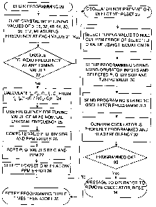
As shown In Figs. 7A and 7B, the controller is initially reset. to a starting
state 11.
The operator then selects Power Vdd, Output Control, Sync and Type for the
oscillator, and
the desired operating frequency 12.
The controller then reads both rows of the device, to determine whether they
are
already programmed 13. Only in rare circumstances can a row of the oscillator
be
reprogrammed, i.e., only where the new program exclusively requires a change
in any bits
from a 0 state to a 1 state. Therefore, the controller is normally reset if
both rows are already
programmed 14. If row 0 is not programmed 14, then the process seeks to
program this row
CA 02372799 2001-10-31
WO 01/61856 PCT/USO1/04783
-19-
17, otherwise, row 1 is programmed 16. If row 1 is to be programmed, the RowO
bit is set to
1 in both rows 0 and 1.
Oscillators may be programmed more than 2 times for a reduced number of
frequencies by searching for P, Q and Divider select by determining values of
each where the
bits previously programmed in row 1 are zero. For example, if the P value in
row 1 is
000100100001 then it could be reprogrammed with any P value that changes a
zero bit to l,
i.e., 100100100001.
If a set of P, Q and Divider select values where only the zero bits are
changed for the
desired new frequency can be found, then the oscillator can be programmed more
than 2
times. There will be a reduced set of these values to select from compared to
un-programmed
parts.
The shadow register of the selected row is then set to values of 0, 16, 32,
48, 64, 80,
96 and 112, sequentially, and the output frequency measured, thus testing the
highest three
bits of tuning values 21. The lower bits are less critical, and generally of
more uniformity, so
actual measurements are generally not required.
In this tuning process, if the output frequency is unreadable 22, the
oscillator is either
not present or defective, and the controller is reset for the next set of
tests 23.
Based on the tuning measurements and the desired output frequency, the values
fR, Co
and C1 are calculated 24 from known fL and C,, per equation 2:
F,=F~*(C1/(2*Co+CL)+1) Eq. 2
The base frequency fR used is, in this case, the tuning value 48 frequency,
allowing
both positive and negative deviations during optimization 25. The set of valid
parameters P,
Q, divider select, and ppm error values are then computed, within the
frequency limits of the
device 26.
The set of valid parameters P, Q are then sorted by Q and ppm 27, and the
lowest Q
value, with a low ppm error is selected 28. In the equation employed by the
phase locked
loop, the P/Q fraction is reduced to simplest form.
The tuning value is then selected to best null out the ppm error of the
selected Q value
29 using the f~ equation.
The programming string established 29 and then sent to the controller,
including P, Q,
divider select, and tuning value 30, which is then programmed into the EPROM
row register
CA 02372799 2001-10-31
WO 01/61856 PCT/USO1/04783
-20-
of the device. The oscillator is then checked to see if it is properly
programmed 33; if not,
the writing of the EPROM is retried up to three additional times 35. If the
device is still not
properly programmed, the operation is aborted. If successfully completed, the
operator is so
informed 34, and the device reset for a new programming cycle.
EXAMPLE 2 - TCVCDCXO
The circuit of Example 1 is modified by substituting the output of an MAS1175
oscillator, shown in Fig. 8, for the crystal in the circuit of Fig. 1B, with
the output of the
MAS1175 connected to the input X~ of the CY2037. Therefore, the tuning
capacitor network
of the CY2037 will be ineffective, and thus need not be present. The
programming device
shown in Fig. 5 is used, with a different oscillator programmer 1 personality
module, shown
in more detail in Figs. 6A and 6B, designed for this part. In particular, the
circuit of Fig. 6B
additionally handles the clock, data, and programming input pins of the MAS
1175. These
signals (along with possibly other test and diagnostic signals) may be brought
to pins on the
oscillator package.
The programming method incorporates the initial CY2037 programming steps shown
in Fig. 7A and the selection of operating and oscillator trimming values as
shown in Fig. 7B,
with the possible exception of the selection of rest trimming values. 1n Fig.
7B, these are
selected as 0, 16, 32, 48, 64, 80, 96, 112, which were found to be optimal for
detecting the
characteristics of the CY2037 tuning network. Rather, for the MAS1175, which
has a 25%
tolerance of the capacitive trimming network, each bit may be tested, e.g., 0,
1, 2, 4, 8, 16, 32,
64, 128, 256, 512, or various bit combinations may be tested. It is noted that
the MAS1175
provides a transparent register mode where the compensation reads either the
values stored in
the EPROM or shift register, allowing the circuit to be functionally tested
prior to
programming.
Prior to performing the steps shown in Fig. 7B, for tuning the oscillator and
selecting
the DCXO coefficients, the temperature compensation parameters are defined. In
fact, the
temperature compensation functions of the MAS1175 may remain unprogrammed
after
calculation, in order to allow greater flexibility in selecting the DCXO
operating parameters.
Fig. 9 shows the measurement of temperature sensitivity, calculation of
parameters, and
programming of the temperature compensation network.
CA 02372799 2001-10-31
WO 01/61856 PCT/USO1/04783
-21-
The measurement of temperature sensitivity involves holding the oscillator
while
operating at a determined temperature, while measuring the output frequency
using an
external frequency reference. The crystal may be placed in an oven or
environmental
chamber, and tested over its operating temperature range, for example
0° to 50° C. Typically,
the oscillator is tested under its rated or nominal load, and allowed to
stabilize prior to taking
a measurement.
As shown in Fig. 9, the oscillator circuit is tested under a plurality of
temperature
conditions, for example at least three temperatures. This data is then used to
calculate the
temperature dependence of the oscillator. The MAS1175 provides parametric
control for
linearity, a cubic term, an inflection point, and a sensitivity (for the
voltage control over the
varactor) .
The programming is initialized 40 by entering a programming mode in the
personality
module of the programmer. The inflection point temperature of the crystal is
then
determined, and inflection point control programmed 41 to compensate for this.
The
frequency offset is then preliminarily compensated 42, but not programmed,
with other
registers temporarily set to intermediate values 43. The varactor sensitivity
is trimmed to a
desired sensitivity 44, using the sensitivity register. With the system
preliminarily trimmed,
the frequency output with at least three different temperatures (inflection
and linearity) or at
least four different temperatures (inflection, linearity and cubic term
sensitivity) is measured
45. The parameter values to achieve a flat frequency response are then
calculated 46. The
circuit may then be tested using the proposed values, prior to programming 47.
The method shown in Fig. 7B is then employed 48 for determining optimal DCXO
parameters and capacitive tuning values. The calculated parameters are then
tested 49 by
operation of the oscillator at room temperature. If these values are not
problematic 50, and if
the values are within tolerance, the various EPROM registers programmed 51. A
message is
then delivered by the programmer 1 to remove the programmed oscillator and
reset the
system 52.
On the other hand, if the determined parameters, especially the divide ratio
Q, are
problematic, i.e., the divide ratio is too high, based on available P, Q,
divide ratio, and tuning
values, then the temperature compensation values may be recalculated 46
seeking to shift the
output frequency sufficient to allow desirable DCXO parameters. In this case,
it is preferred
CA 02372799 2001-10-31
WO 01/61856 PCT/USO1/04783
-22-
that, after recalculation of the temperature compensation parameters, that the
oscillator be
verified for operation over temperature 49, since the temperature compensation
values will be
non-optimal. For example, by adjusting the cubic sensitivity term, inflection
point, and
linearity, a new operating point may be achieved which alters the crystal
operating frequency
yet which meets functional tolerances and specifications.
EXAMPLE 3
Fig. 10A shows a prior art packaged oscillator having an external power supply
bypass capacitor. Typically, packaged PLL oscillators has relied on external
bypass
capacitors. Some known non-PLL oscillators have included internal bypass
capacitors, in
larger package sizes. Fig. lOB shows a packaged PLL oscillator having an
internal power
supply bypass capacitor according to the present invention. According to this
embodiment, a
10-100 nF chip capacitor is provided within the oscillator housing for power
supply
bypassing.
Figs. 11A and 11B, and 11C and 11D shows, respectively, comparative tracings
of the
fitter distributions between the comparative example of Fig. 10A and the
example of Fig. lOB
for 100 MHz (Figs. 11A and 11B) and 40 MHz (Figs. 11C and 11D) PLL
oscillators,
respectively. In each case, the non-bypassed oscillator displays a bimodal (or
in some cases,
not shown, a trimodal distribution), while the PLL oscillators with internal
bypass capacitors
have lower overall fitter with a Gaussian distribution.
These fitter measurements were obtained using an HPE3631A Power Supply,
feeding
an oscillator under test under rated load in a test fixture. A LeCroy LC684DXL
Oscilloscope
with PP096 8 GS/S adapter, with an input from an HP 1144A Active Probe with HP
1142
Power supply acting as input. A 10 MHz timebase is provided by an HP 53121A
Frequency
Counter. The Oscilloscope and Frequency Counter communicate with a personal
computer
using a GPIB control bus.
Each horizontal division is 10.0 i. Fig. 1 1A represents 25,972 fitter counts,
Fig. 11B
represents 25,973 fitter counts, Fig. 11C represents 25,086 fitter counts and
Fig. 11D
represents 25,036 fitter counts. Each oscillator was tested with a supply
voltage of 3.3 V and
an output load of 15 pF (100 MHz) or 30 pF (40 MHz).
CA 02372799 2001-10-31
WO 01/61856 PCT/USO1/04783
-23-
For Fig. 11A, the period is 30.519 ns, the low is 30.4143 ns, the high is
30.5878 ns,
the range is 173.50 ps and the sigma is 43.21 ps. For Fig. 11B, the period is
30.519 ns, the
low is 30.4798 ns, the high is 30.5523 ns, the range is 72.50 ps and the sigma
is 10.06 ps. For
Fig. 11C, the period is 24.998 ns, the low is 24.8966 ns, the high is 25.0636
ns, the range is
167.00 ps and the sigma is 23.23 ps. For Fig. 11D, the period is 24.999 ns,
the low is
24.9416 ns, the high is 25.0516 ns, the range is 110.00 and the sigma is 12.29
ps.
Fig. 12 shows a comparison of phase fitter measurements between an externally
bypassed embodiment (Fig. 10A), an internally bypassed embodiment (Fig. 10B),
over a
range of frequencies. As shown in Fig. 12, the non-bypassed PLL oscillator
represented in
the upper tracing always has greater fitter than the internally bypassed PLL
oscillator, over a
broad range of frequencies.
While the above detailed description has shown, described and pointed out the
fundamental novel features of the invention as applied to various embodiments,
it will be
understood that various omissions and substitutions and changes in the form
and details of the
system and method illustrated may be made by those skilled in the art, without
departing
from the spirit of the invention. Consequently, the full scope of the
invention should be
ascertained by the appended claims.