Note: Descriptions are shown in the official language in which they were submitted.
CA 02372915 2002-03-11
' 1
Cipher Processing Apparatus, IC Card and Cipher Processing Method
This application is a divisional application of Canadian Patent Application
Serial
Number 2,261,161 filed on April 24, 1998.
Technical Field
The present invention relates to a cipher processing apparatus, in particular,
to a small-
sized cipher processing apparatus installed in an IC (Integrated Circuit) card
and so on.
Background Art
For a conventional related art of the invention, DES (Data Encryption
Standard) of
U.S. commercially used cipher, which is a block cipher of secret key (common
key)
cryptosystem, will be explained.
A detail of DES processing is described in such as Hans Eberl "A High-speed
DES
implementation for Network Applications", Advances in Cryptology - CRYPTO '92,
Lecture
Notes in computer Science 740, Springer-Verlag.
Fig. 18, is a flowchart showing DES encryption algorithm.
In Fig. 18, reference numerals 1001 - 1004 show operations using function F
for data
transformation. Reference numerals 1011 - 1014 show XOR operations bit by bit.
In the
figure, an initial permutation and a final permutation are omitted.
An operation will be explained.
CA 02372915 2002-03-11
2
- An input data 1050 having 2 X n bits (in case of DES, 2 X 32 bits) is
divided into two n-bit data 1051 and 1052: The n-bit data 1051 is output as
n-bit data 1053 without any transformation. The data 1051 is also input to
the function F 1001 to be transformed. The data transformed by the
function F 1001 is XORed with the other n-bit data 1052 bit by bit by the
XOR operation 1011 and the XORed result is output as n-bit data 1054.
Hereinafter, operations are repeated by the functions F 1002, 1003,
and 1004, the XOR operations .1012, 1013, and 1014 and output data 1055
and 1056 are output. The two n-bit data are united and output as 2n-bit
data 1057.
Fig. 19 shows an example of cipher processing apparatuses
performing data transformation similar to the DES encryption as shown in
the flowchart of Fig. 18.
In Fig. 19, reference numerals 1101 and 1102 show registers A and B
for holding data. Reference numerals 1103 and 1104 are selectors A and B
for selecting one of data. 1105 denotes a function F operating circuit for
calculating the function F as data transformation. 1106 denotes an XOR
circuit. 1201 and 1202 respectively show n-bit input data A and B. 1203
and 1204 respectively show n-bit output data A and B.
An operation will be explained.
An input data having 2 X n bits (in case of DES, 2 X 32 bits) is divided
into two n-bit input data A1201 and B1202. The two input data are
respectively selected by the selectors A1103 and B1104 and held in the
registers A1101 and B1104. The data held in the register A1101 is fed back
to the selectors A1103 and B1104 and input to the function F operating
CA 02372915 2002-03-11
3
circuit 1105 at the same time. After transformed by the function F
operating circuit 1105, the data is XORed by the XOR circuit x106 with the
data held in the register B1102. The XORed result is fed back to the
selectors A1103 and B1104.
Next, the selector A1103 selects the XORed result of the XOR circuit
1106, the selector B selects data held in the register A1101, and the
registers
A1001 and B1002 are respectively updated by these selected data to hold
therein. Then, similarly, the operation, corresponding to the operation
through the functions F 1002, 1003, 1004 and the XOR circuits 1012, 1013,
1014 shown in Fig. 18, is repeated (looped) a necessary number of times, and
the output data A1203 and B1204 are finally output. In case of DES, the
operation will be repeated 16 times.
This conventional related art is described in detail, for example, in
Hans Eberl "A High-speed DES Implementation for Network Applications",
Advances in Cryptology-CRYPTO '92, Lecture Notes in computer Science 740,
Springer-Verlag.
In a cipher processing apparatus by the above method, when the
apparatus is constructed by a plurality of the functions F having similar
configuration for processing, it is possible to efficiently construct a
processing
circuit by using one circuit repeatedly This enables to reduce the circuit
scale and also save electric power. However, there is a problem that when
the function F includes a smaller circuit having repeating process, the
conventional configuration of the cipher processing apparatus does not
efficiently reduce the circuit scale or save electric power.
The present invention is provided to solve the above-mentioned
CA 02372915 2002-03-11
4
problem. The invention aims to obtain a cipher processing apparatus, which can
be
constructed efficiently to reduce a circuit scale and save electric power even
if the
apparatus has a configuration of repeatedly processing the function F
including an
internal smaller circuit configured by repeating process.
Disclosure of the Invention
In accordance with one aspect of the present invention there is provided an
IC (integrated circuit) card communicating data with a reader/writer
comprising: a
data receiving circuit receiving the data from the reader/writer; a data
transmitting
circuit transmitting the data to the reader/writer; and a cipher processing
apparatus
for inputting data A and data B to be encrypted, having a first operating unit
for
alternately performing a first data transformation on the data A and the data
B; and
a second operating unit for performing a second data transformation on one of
the
data A and the data. B input to the first operating unit inside of the first
operating
unit, encrypting the data A and the data B by repeatedly operating the second
operating unit inside of the first operating unit and by repeatedly operating
the first
operating unit; and outputting an encrypted data A and an encrypted data B;
the
cipher processing apparatus comprising: a register A for inputting and holding
the
data A to be encrypted, holding and outputting the data A to be input to the
first
operating unit, and outputting the encrypted data A after repeatedly operating
the
first operating unit; a register B for inputting and holding the data B to be
encrypted, holding and outputting the data B to be input to the first
operating unit,
and outputting the encrypted data B after repeatedly operating the first
operating
unit; a register C, provided inside of the first operating unit, for
repeatedly holding
and outputting the data C output from the second operating unit; a selector C
for
selecting one of the register A, the register B and the register C, and
outputting the
data held in the register selected; an XOR circuit A for XORing the data
output by
the selector C with the data A held in the register A; a selector A for
selecting a
CA 02372915 2002-03-11
result XORed by the XOR circuit A, outputting the result to the register A to
make
the register A hold the result; an XOR circuit B for XORing the data output by
the
selector C with the data B held in the register B; and a selector B for
selecting a
result XORed by the XOR circuit B, outputting the result to the register B to
make
the register B hold the result; wherein the first operating unit includes the
second
operating unit, the register C and the selector C; wherein the second
operating unit,
the register C and the selector C form a first processing loop inside of the
first
operating unit for repeatedly performing the second data transformation by the
second operating unit; and wherein the first operating unit forms the second
processing loop with the XOR circuits A and B, the selectors A and B, and the
registers A and B for repeatedly performing the first data transformation by
the first
operating unit; wherein the second operating unit inputs the data output from
the
selector C, performs the second data transformation on the data, outputs the
data to
the register C to make the register C hold the data as data C; wherein the
selector C
alternately selects the data A held in the register A and the data B held in
the
register B to output to the second operating unit to make the first operating
unit
repeatedly perform the first data transformation alternately on the data A and
the
data B with making the second operating unit start repeatedly performing the
second data transformation in case of repeatedly operating the first operating
unit;
the selector C selects the data C held in the register C to output to the
second
operating unit to make the second operating unit repeatedly perform the second
data
transformation in case of repeatedly performing the second data transformation
by
the second operating unit; and the selector C selects the data C held in the
register C
to output to the XOR circuits A and B, and makes the XOR circuits A and B XOR
in case of terminating the second data transformation by the second operating
unit
being performed repeatedly; wherein the selectors A and B alternately select
the
result XORed by the XOR circuit A and the result XORed by the XOR circuit B
CA 02372915 2002-03-11
6
and output the result to the registers A and B, and make the registers A and B
and
alternately hold the result in case of terminating the second data
transformation by
the second operating unit being performed repeatedly.
In accordance with another aspect of the present invention there is provided
an IC card communicating data with a reader/writer comprising: a data
receiving
circuit receiving the data from the reader/writer; a data transmitting circuit
transmitting the data to the reader/writer; and a cipher processing apparatus
for
inputting data A and data B to be encrypted having a first operating unit for
alternately performing a first data transformation on the data A and the data
B; and
a second operating unit for performing a second data transformation on one of
the
data A and the data B input to the first operating unit inside of the first
operating
unit; encrypting the data A and the data B by repeatedly operating the second
operating unit inside of the first operating unit and by repeatedly operating
the first
operating unit, and outputting an encrypted data A and an encrypted data B,
the
cipher processing apparatus comprising: an input line A for inputting the data
A to
be encrypted, an input line B for inputting the data B to be encrypted, an
output line
A for outputting the encrypted data A; and an output line B for outputting the
encrypted data B; registers A, B and C for holding data; selectors A, B and C
for
selecting data; and XOR circuits A and B, wherein the first operating unit
includes
the selector C and the register C and the second operating unit; wherein the
register
A is connected to an output side of the selector A, and also connected to the
output
line A for outputting the data A, an input side of the selector C and a input
side of
the. XOR circuit A; wherein the register B is connected to an output side of
the
selector B, and also connected to the output line B for outputting the data B,
an
input side of the selector C and an input side of the XOR circuit B; wherein
to
selector A is connected to the input line A for inputting the data A and an
output
side of the XOR circuitA, and also connected to an input side of the register
A; and
CA 02372915 2002-03-11
7
the selector A inputs the data A from the input line A and outputs the data A
to
make the register A hold the data A in case of initiating a first operation of
the first
operating unit; wherein the selector B is connected to the input line B for
inputting
the data B and the output side of the XOR circuit B, and also connected to an
input
side of the register B; and the selector B inputs the data B from the input
line B and
outputs the data B to make the register B hold the data B in case of
initiating the
first operation of the first operating unit; wherein the selector C is
connected to an
output side of the register A, an output side of the register B and an output
side of
the register C, and also connected to an input side of the second operating
unit, an
input side of the XOR circuit A and an input side of the XOR circuit B;
wherein the
second operating unit is connected to an output side. of the selector C, and
also
connected to an input side of the register C; and the second operating unit
performs
the second data transformation on the data selected by the selector C and
outputs a
result of the second data transformation to make the register C hold the
result as
data C; wherein the register C is connected to an output side of the second
operating
unit, and also connected to an input side of the selector C; wherein the XOR
circuit
A is connected to an output side of the selector C and an output side of the
register
A, and also connected to an input side of the selector A; the XOR circuit A
XORs
the data C output from the selector C with the data A held in the register A
and
outputs an XORed result to the selector A; wherein the XOR circuit B is
connected
to an output side of the selector C and an output side of the register B, and
also
connected to an input side of the selector B; the XOR circuit B XORs the data
C
output from the selector C with the data B held in the register B and outputs
an
XORed result to the selector B; wherein the selector C selects the data A held
in the
register A and outputs the data A to the second operating unit, the XOR
circuit A
and the XOR circuit B in case of initiating an odd-numbered operation of the
first
operating unit; the selector C selects the data B held in the register B and
outputs
CA 02372915 2002-03-11
7a
the data B to the second operating unit, the XOR circuit A and the XOR circuit
B in
case of initiating an even-numbered operation of the first operating unit; and
the
selector C selects the data C held in the register C and outputs the data C to
the
second operating unit, the XOR circuit A and the XOR circuit B in case of
repeatedly operating the second operating unit or terminating the second
operating
unit being operated repeatedly; wherein the selector A does not select the
result
XORed by the XOR circuit A to make the register A hold the data A as it is in
case
of terminating the odd-numbered operation of the first operating unit; and the
selector A selects the result XORed by the XOR circuit A to make the register
A
hold the result as the data A in case of terminating the even-numbered
operation of
the first operating unit; and wherein the selector B does not select the
result XORed
by the XOR circuit B to make the register B hold the data B as it is in case
of
terminating the even-numbered operation of the first operating unit; and the
selector
B selects the result XORed by the XOR circuit B to make the register B hold
the
result as the data B in case of terminating the odd-numbered operation of the
first
operating unit.
Brief Description of the Drawings
Fig. 1 shows an encryption algorithm in relation to a first embodiment of the
present invention.
Fig. 2 shows a configuration of a function used for an encryption
CA 02372915 2002-03-11
8
algorithm in relation to the first embodiment of the present invention.
Fig. 3 is a block diagram showing a basic configuration of a cipher
processing apparatus according to the first embodiment of the invention.
Fig. 4 is a flowchart showing one example of basic operations of the
cipher processing apparatus according to the first embodiment of the
invention.
Fig. 5 is a flowchart showing one example of basic operations of the
cipher processing apparatus according to the first embodiment of the
invention.
Fig. 6 shows a configuration of the function used for an encryption
algorithm in relation to the first embodiment of the present invention.
Fig. 7 shows the encryption algorithm according to the first
embodiment of the present invention.
Fig. 8 shows a configuration of the function used for the encryption
algorithm according to the first embodiment of the present invention.
Fig. 9 is a block diagram showing a configuration of a second
operating circuit according to the first embodiment of the present invention.
Fig. 10 shows an encryption algorithm in relation to a second
embodiment of the present invention.
Fig. 11 shows a confrguration of a function used for the encryption
algorithm according to the second embodiment of the present invention.
Fig. 12 is a block diagram showing a basic configuration of a cipher
processing apparatus according to the second embodiment of the invention.
Fig. 13 is a flowchart showing an example of basic operations of the
cipher processing apparatus according to the second embodiment of the
CA 02372915 2002-03-11
9
invention.
Fig. 14 is a flowchart showing one example of basic operations of the
cipher processing apparatus according to the second embodiment of the
invention.
Fig. 15 is a flowchart showing an example of basic operations of the
cipher processing apparatus according to the second embodiment of the
invention.
Fig. 16 is a block diagram showing a basic configuration of a
communication system according to a third embodiment of the invention.
l0 Fig. 17 is a block diagram showing a basic configuration of an IC
according to the third embodiment of the invention.
Fig. 18 shows an encryption algorithm according to the conventional
related art.
Fig. 19 is a block diagram showing a basic configuration of a cipher
processing apparatus according to the conventional related art.
Best Mode for Carrying out the Invention
Embodiment 1.
A cipher processing apparatus according to one embodiment of the
present invention will be explained referring to Figs. 1 through 3.
Fig. 1 is a flowchart showing an encryption algorithm of a cipher
processing apparatus according to one embodiment of the present invention.
In Fig. 1, reference numerals 101 through 104 show operations using
functions F for data transformation, and reference numerals 111 through 114
show XOR operations bit by bit.
CA 02372915 2002-03-11
Fig. 2 shows a configuration of operation using the . function F, which
is configured by three operations using functions f 201 through 203 and an
operation using a function g 211.
An operation will be described hereinafter.
5 An input data 150 having 2 X n bits is divided into two, namely, n-bit
data 151 having upper digits of the input data and n-bit data 152 having
lower digits of the input data. The n-bit data 151 is output as n-bit data 153
without any transformation, and the n-bit data 151 is also transformed by
the function F 101. The output data from the function F 101 is XORed with
10 another n-bit data 152 by the XOR circuit 111 bit by bit and n-bit data 154
is
output. In the function F, three operations using the functions f 201
through 203 are performed, an operation using the function g 211 is then
performed and the result is output.
Then, similarly, operations are repeated through the functions F 102,
103, 104, and XOR circuits 112, .113, 114 and n-bit data 155, 156 are output.
The two n-bit data are united and output as 2n-bit data 15'7.
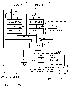
Fig. 3 shows a general configuration of the cipher processing
apparatus embodying the algorithm for data transformation explained by
referring to Figs. 1 and 2.
In Fig. 3, reference numerals 301, 302 and 303 respectively show a
register A, a register B and a register C. Reference numerals 311, 312 and
313 respectively show a selector A, a selector B and a selector C. 321 and
322 denote bit by bit XOR circuits. 323 denotes a function f operating
circuit, which is one of configurational elements performing the function F
operation. 324 denotes a function g operating circuit, which is one of
CA 02372915 2002-03-11
11
configurational elements performing the function F operation.
The register C 303, the ;selector C 313, the function f operating circuit
323 and the function g operating circuit 324 form a first operating circuit
100.
The register C 303, the selector C 313, the function f operating circuit 323
form a loop processing circuit 200.
Figs. 4 and 5 are flowcharts showing an operation of the circuits
shown in Fig. 3.
The operation will be explained by referring to Figs. 4 and 5.
The operation by the function F is performed by three-times
operation of the function f operating circuit and once operation of the
function g operating circuit.
Data transformation at a first stage shown in Fig. 1 will be
explained.
An input data having 2 X n bits is divided into two n-bit data, namely,
an input data A 351 and an input data B 352. The input data axe selected
by the selector A 311 and the selector B 3I2, and held in the register A 301
and the register B 302 (at step 4-1).
Then, in the selector C 313, it is detected whether this is a process of
an odd-numbered stage or a process of an even-numbered stage (at step 4-2),
the data held in the register A 301 is selected (at step 4-4), and the
selected
data is transformed by the function f operating circuit 323 (at step 4-6). The
output data from the function f operating circuit 323 is held in the register
C
303 (at step 4-7). A first operation by the function f operating circuit ends
with this step.
Then, in the selector C 313, the data held in the register C 303 is
CA 02372915 2002-03-11
12
selected (at step 4-8), and the selected data is transformed by the function f
operating circuit 323 (at step. 4-6). The data output from the function f
operating circuit 323 is held in the register C 303 (at step 4-7): With this
step, a second operation by the function f operating circuit ends.
Further, in the selector C 313, the data held in the register C 303 is
selected (at step 4-8). The selected data is transformed by the function f
operating circuit 323 (at step 4-6), and the transformed data is held in the
register C 303 (at step 4-7). With this step, a third operation by the
function
f operating circuit 323 ends.
Next, in the selector C 313, the data held in the register C 303 is
selected (at step 4-9}: The selected data is transformed by the function g
operating circuit 324 and the result is output (at step 4-10). With this step,
a whole operation by the function F terminates.
Next, it is detected whether this is a process of an odd-numbered
stage or a process of an even-numbered stage (at step 4-11), the data output
from the function g operating circuit 324 is fed back to be XORed with the
data held in the register B 302 by the XOR circuit 322 (at step 4-14). The
XORed data is selected by the selector B 312 and the selected data is held in
the register B 302 (at step 4-I5). This step completes the first stage of the
data transformation.
Next, a second stage of the data transformation will be explained.
It is detected to be an even-numbered stage (at step 4-2), and the
selector C 313 selects the data held in the register B 302 (at step 4-3).
Then,
the selected data is transformed by the function f operating circuit 323 (at
step 4-6), and the output data is held in the register C 303 tat step 4-7). A
CA 02372915 2002-03-11
13
first operation by the function f operating cixcuit ends with this step.
Then, in the selector C, 313, the data held in the register C 303 is
selected (at step 4-8), and the selected data is transformed by the function f
operating circuit 323 (at step 4-6). The data output from the function f
operating circuit 323 is held in the register C 303 (at step 4-7). With this
step, a second operation by the 'function f operating circuit 323 ends.
Further, in the selector C 313, the data held in the register C 303 is
selected (at step 4-8). The selected data is transformed by the function f
operating circuit 323 (at step 4-6), and the transformed data is held in the
register C 303 (at step 4-7). With this step, a third operation by the
function
f operating circuit 323 ends.
Next, in the selector C 313, the data held in the register C 303 is
selected (at step 4-9). The selected data is transformed by the function g
operating circuit 324 and the result is output (at step 4-10). With this step,
a whole operation by the function F circuit terminates.
Next, it is detected to be a process of an even-numbered stage (at step
4-11), the data output from the function g operating circuit 324 is fed back
to
be XORed with the data held in the register A 301 by the XOR circuit 321 (at
step 4-12). The XORed data is selected by the selector A 311 and the
selected data is held in the register A 301 (at step 4-13). This step
completes the second stage of the data transformation.
Hereinafter, similar processes to the first stage of the data
transformation and the second data transformation will be alternately
repeated a necessary number of times.
Finally, the data held in the registers A 301 and B 302 are output as
CA 02372915 2002-03-11
14
output data A 353 and output data B 354 as a result of the data
transformation of the final stage (at step 4-19).
As has been described, according to this invention; the one function f
operating circuit 323 can be used repeatedly by providing the register C 303
and the selector C 313. The cipher processing apparatus does not need to
include three function f operating circuits, but need to include only one
function f operating circuit 323, which reduces a circuit scale.
Especially, the function F (the function f, the function g), used for the
data transformation for cipher processing, is known to have an extremely
complex configuration because the data transformation for cipher processing
requires to use a function being strong against cryptanalysis. Hence, the
reduction of the circuit scale according to the present invention effects a
lot
to the data transformation for cipher processing.
According to the invention, it is not always required to operate the
register A 301, the register B 302, the register C 303, the selector A 311,
the
selector 312, and the selector C 313. The processes can be performed with
these circuits operating only when required, which enables the apparatus to
save electric power.
Accordingly, this invention takes a great effect when applied to a
small apparatus such as an IC card. The invention can be applied not only
to the IC card, but also to a reader/writer for the IC card.
The function F is not limited to have the above configuration. For
example, when the function F is configured by only repeating the operation
of function f as shown in Fig. 6, the function g is not needed for the
configuration of Fig. 3. In this case, the data selected by the selector C 313
CA 02372915 2002-03-11
is directly fed back as shown in Fig. ?.
When the function f operating circuit 323 includes m (m > 1) number
of functions, which constitute in an arbitrary order, as shown in Fig. 8, the
m
number of functions are aligned in parallel at a place corresponding to the
5 function f operating circuit 323 of Fig. 3. The data is input to each of the
m
number of functions from the selector C 313, the output data from the rn
number of functions axe input to the selector with m number of inputs and
one output, and the selector selects one output data to be held in the
register
C 303 as shown in Fig. 9. These operations are repeated a number of times
10 corresponding to an arbitrary order of the m number of functions.
Embodiment 2.
A cipher processing apparatus according to another embodiment of
the present invention will be explained referring to Figs. 10 through 14.
Fig. 10 shows a flowchart of MISTY encryption algorithm.
15 Details of MISTY is disclosed in, for example, Mitsuru Matsui "Block
Encryption Algorithm MISTY", the Institute of Electronics, Information and
Communication Engineers, Technical Report ISEC 96-11 (1996-07).
In Fig. 10, reference numerals 501 through 506 denote operations by
functions FL, reference numerals 511 through 514 denote operations by
functions FO, and 521 through 524 are XOR operations.
Fig. 11 shows operations using the functions FO 511 through 514 of
Fig. 10.
As shown in Fig. 11, in MTSTY algorithm, transformation process,
including functions FI 601 through 603 and XOR operations 611 through 613,
is repeated three times as operations by the functions FO 511 through 514.
CA 02372915 2002-03-11
16
Fig. 12 shows one embodiment of a cipher processing apparatus
applying the data transformation process of MISTY of Figs. 10 and 11
according to the present invention.
In the following, an operation of the encryption algorithm of Figs. 10
and 11 will be explained.
An input data 550 having 2 X n bits is divided into two n-bit data, one
having upper n digits of the input data 550 and the other having lower n
digits of the input data 550, and the two divided data are input as an input
data A 551 and an input data B 5~2. In case of MISTY, n=32. After
transformed by the function FL, 501, the n-bit input data 551 is output as n-
bit data 553, and is also transformed by the function FO 511. The other n-
bit input data 552 is transformed by the function FL 502. The data
transformed by the function FO 511 is XORed bit by bit by the XOR
operation 521 with the output data from the function FL 502, and n-bit data
554 is output. In the function FO, operations by the functions FI 601
through 603 and the XOR operations 611 through 613 are performed.
Namely, the input 2m-bit data (n bits) 650 is divided into two m-bit data 651
and 652. After transformed by the function FI, the data 651 is XORed bit by
bit by the XOR operation 611 with the data 652, and the XORed result is
output as data 653. The data 652 is output as data 654 without any
transformation. Hereinafter, the above operations are repeated in three
stages. Finally, two m-bit data are united and output as 2m-bit (n bits) data
655.
Next, an operation at a second stage will be described.
The output data 554 supplied from the first stage is output without
CA 02372915 2002-03-11
17
any transformation, and at the same time, is transformed by the function FO
512. The output data from the function FO 512 is XORed bit by bit by the
XOR operation 522 with the other n-bit data 553, and the XORed result is
output.
Hereinafter, data transformation similar to the process of the first
and second stages is repeated a necessary number of times, and n-bit data
557 and 558 are output. Finally, the output data is transformed by FL
functions 505 and 506 into data, of which the upper digits and the lower
digits are exchanged, the two n-bit data are united, and 2n-bit data 559 is
outp ut.
Fig. 12 shows a general configuration of the cipher processing
apparatus embodying the data transformation algorithm explained by
referring to Figs. 10 and 11.
In Fig. 12, reference numerals 701, 702, 703 denote a register A, a
register B, and a register C, respectively. Reference numerals 711, 712, 713,
714 denote a selector A, a selector B, a selector C, and a selector D. 721,
722,
723 show XOR circuits, 724 shows a function FI operating circuit for data
transformation, and 725 shows a function FL operating circuit for data
transformation_ 751 is an input data A, 752 is an input data B, 753 is an
output data A, and 754 is an output data B.
Here, the register C 703, the selector C 713; the function FI operating
circuit 724 and the XOR circuit 723 constitute a first operating circuit 101
fox
a first data transformation. The register C 703, the selector C 713, the
function FI operating circuit 724; and the XOR circuit 723 constitute a loop
processing circuit 201.
CA 02372915 2002-03-11
18
Figs. 13 through 15 are flowcharts explaining an operation of the
cipher processing apparatus shown in Fig. 12.
The operation will be described by referring to Figs. 13 through 15.
First, an input data having 2 X n bits is divided into two n-bit data,
and input as an input data A 751 and an input data B 752. In case of
MISTY, n=32. The two input data are respectively selected by the selector
A 711, the selector B 712 and respectively held in the register A 701, the
register B 702 (at step 8-1).
Next, in the selector C 713, it is detected whether this is a process of
an odd-numbered stage or a process of an even-numbered stage (at step 8-2),
and the data held in the register A 701 is selected (at step 8-3). Then, the
selected data is transformed by the function FL operating circuit 725 (at step
8-4), and the output data is selected by the selector D 714 (at step 8-5).
Further, the selected data is selected by the selector A '711 (at step 8-6),
and
is held in the register A 701 (at step 8-'7).
Next, in the selector C 713, the data held in the register B 702 is
selected (at step 8-8). The selected data is transformed by the function FL
operating circuit 725 (at step 8-9), and the output data is selected by the
selector D 714 (at step 8-10). Further, the selected data is selected by the
selector B 712 (at step 8-11), and is held in the register B (at step 8-12).
Next, in the selector C 713, the data held in the register A '701 is
selected (at step 8-13). Then, the selected data (2 X m bits) is divided into
two m-bit data, and one m-bit data is output as an output data without any
transformation. The other m-bit data is input to the function FI operating
circuit '724 to be transformed. The transformed data is XORed bit by bit by
CA 02372915 2002-03-11
19
the XOR circuit 723 with the other m-bit data, and the XORed result and the
output m-bit data are united (at step 8-14). The united output data is held
in the register C 703 (at step 8-15). With this step, a first process
including
the function FI operating circuit 724 has been completed.
Next, in the selector C 713, the data held in the register C 703 is
selected (at step 8-16). The selected data (2 X m bits) is divided into two m-
bit data, and one m-bit data is output as an output data without any
transformation. The other m-bit data is input to the function FI operating
circuit 724 to be transformed. The transformed data is XORed bit bybit by
the XOR circuit 723 with the other m-bit data, and the XORed result and the
output m-bit data are united (at step 8-14). The united output data is held
in the register C 703 (at step 8-15). With this step, a second process
including the function FI operating circuit 724 has been completed.
Next, in the selector C 713, the data held in the register C 743 is
selected (at step 8-16). The selected data (2 X m bits) is divided into two m-
bit data, and one m-bit data is output as an output data without any
transformation. The othex m-bit data is input to the function FI operating
circuit 724 to be transformed. The transformed data is XORed bit by bit by
the XOR circuit 723 with the other m-bit data, and the XORed result and the
output m-bit data are. united (at step 8-14). The united output data is held
in the register C 703 (at step 8-15). With this step, a third process
including
the function FI operating circuit 724 has been completed.
Next, in the selector C 713, the data held in the register C '703 is
selected (at step 8-16), and the selected data is selected by the selector D
714
(at step 8-18). Then, it is detected whether this is a process of an odd
CA 02372915 2002-03-11
numbered stage or a process of an even-numbered stage (at step 8-19), the
selected data is fed back, and is XORed by the XOR circuit ?22 with the data
held in the register B 702 (at step 8-20). The output data from the XOR
circuit B ?02 is selected by the selector B 712 (at step 8-21), and is held in
the
5 register B ?02 (at step 8-22). With this step, the data transformation
process of the first stage terminates.
Next, a data transformation process corresponding to the data
transformation process of the second stage shown in Fig. 10 is performed.
First, in the selector C ?13, it is detected to be an even-numbered
10 stage (at step 8-2); and the data held in the register B 702 is selected
(at step
8-24).
The selected data (2 X m bits) is divided into two m-bit data, and one
m-bit data is output as an output data without any transformation: The
other m-bit data is input to the function FI operating circuit ?24 to be
15 transformed. The transformed data is XORed bit by bit by the XOR circuit
723 with the other m-bit data, and the XORed result and the output m-bit
data are united (at step 8-14). The united output data is held in the register
C 703 (at step 8-15). With this step, a first process including the function
FI
operating circuit ?24 has been completed.
20 Next, in the selector C '713, the data held in the register C ?03 is
selected (at step 8-16). The selected data (2 X m bits) is divided into two m-
bit data, and one m-bit data is output as an output data without any
transformation. The other m-bit data is input to the function FI operating
circuit ?24 to be transformed. The transformed data is XORed bit by bit by
the XOR circuit?23 with the other m-bit data; and the XORed result and the
CA 02372915 2002-03-11
21
output m-bit data are united (at step 8-14). The united output data is held
in the register C 703 (at step 8-15). With this step, a second process
including the function FI operating circuit 724 has been completed.
Next, in the selector C ?13, the. data held in the register C ?03 is
selected (at step 8-16). The selected data (2 X m bits) is divided into two or
bit data, and one m-bit data is output as an output data without any
transformation. The other m-bit data is input to the function FI operating
circuit ?24 to be transformed. The transformed data is XORed bit by bit by
the XOR circuit ?23 with the other m-bit data, and the XORed result and the
output m-bit data are united (at step 8-14). The united output data is held
in the register C 703 (at step 8-15). With this step, a third process
including
the function FI operating circuit ?24 has been completed.
Next, in the selector C ?13, the data held in the register C ?03 is
selected (at step 8-16), and the selected data is selected by the selector D
?14
(at step 8-18). Then, it is detected to be an even-numbered stage (at step 8
19), the selected data is fed back, and is XORed bit by bit by the XOR circuit
?21 with the data held in the register A ?O1 (at step 8-25). The output data
from the XOR circuit A ?21 is selected by the selector A ?11 (at step 8-26),
and is held in the register A ?01 (at step 8-2?). With this step, the data
transformation process of the second stage terminates.
Hereinafter, data transformation process similar to the data
transformation processes of the first stage and the second stage is repeated
alternately a necessary number of times. MISTY performs up to a
transformation process corresponding to the transformation process of an
eighth stage.
CA 02372915 2002-03-11
22
Then, a process of step 8-28 is performed. At step 8-28, the above
steps $-3 through 8-12 are performed. First, in the selector C 713, the data
held in the register A 701 is selected (at step 8-3). Next, the selected data
is
transformed by the function FL operating circuit 725 (at step 8-4), and the
output data is selected by the selector D 714 (at step 8-5). Further, the
selected data is selected by the selector A 711 (at step 8-6), and is held in
the
register A 701 (at step 8-7).
Next, in the selector C 713, the data held in the register B 702 is
selected (at step 8-8). The selected data is transformed by the function FL
operating circuit 725 (at step 8-9), the output data is selected by the
selector
D 714 (at step 8-10). Further, the selected data is selected by the selector B
712 (at step 8-11), and is held in the register B (at step 8-12).
Finally, the data held in the register A 701 and the register B 702 are
output as an output data A 753 and an output data B 754 (at step 8-29).
According to this embodiment, the cipher processing apparatus does
not need to include three function FI operating circuits and three XOR
circuits even when the functions FO 511 through 514 of each stage has such
a configuration as shown in Fig. 11. It is enough for the cipher processing
apparatus to include only one function FI operating circuit and one XOR
circuit, which enables to reduce a circuit scale. Further, the ciphex
processing apparatus does not need to include a plurality of circuits for the
functions FL 501 through 504 even when the cipher algorithm has a
configuration as shown in Fig. 10. It is enough fox the cipher processing
apparatus to include only one function FL operating circuit, which also
enables to reduce a circuit scale.
CA 02372915 2002-03-11
23
In case of MISTY of this embodiment, a function used for the function
FI and the function FL should be strong against cryptanalysis, so that the
function has an extremely complex configuration: Hence, the reduction of
the circuit scale according to the present invention is quite effective.
Further, as clearly understood by the above description of the
embodiment, it is not always required to operate the registers A through C,
and the selectors A thxough D: The process can be performed with these
circuits operating only when required, which takes a great effect on saving
electric power.
Accordingly, it is very effective to apply this invention to a small
apparatus such as an IC card'. The invention can be applied not only to the
IC card, but also to a reader/writer for the IC card.
Embodiment 3.
Figs. 16 and I7 show general configurations of communication
system of one embodiment of the present invention.
In Figs: 16 and 17, a reference numeral 91 shows a reader/writer, a
reference numeral 92 shows an IC (integrated circuit) card, and 93 shows an
IC of the IC card 92. The IC 93 includes configurational elements: a
transmitter/receiver 94 for transmittinglreceiving communication data; a
CPU (central processing unit) 95 for controlling the apparatus; a memory 96
for storing data and pxogram, etc.; and a cipher processing apparatus 9'l for
encrypting/decrypting a communication data. The IC 93 includes the
transmitter/receiver 94, the CPU 95, the memory 96, and the cipher
processing apparatus 9'7 as configurational elements.
The cipher processing apparatus described in the first ox the second
CA 02372915 2002-03-11
24
embodiment is applied to the cipher processing apparatus 97.
In this communication system; the encrypted data is transmitted.
Namely, in the IC card 92, the transmitter/receiver 94 transmits data
encrypted by the cipher processing apparatus 97 to the reader/writer 91.
The transmitter/receiver 94 also receives data transmitted from the
reader/writer 91, and the received data is decrypted by the cipher processing
apparatus 9'7 to implement communication:
In this case, communication between the reader/writer 91 and the IC
card 92 can be either connected or unconnected.
Industrial Applicability
As has been described, according to the invention, in the
communication system using encrypted data, the circuit scale of the cipher
processing apparatus can be reduced and the electric power can be saved.
Further, an IC card can be effectively configured by applying the
cipher processing apparatus of the invention. The reduction of the circuit
scale and the saving electric power has been performed in the IC card.