Note: Descriptions are shown in the official language in which they were submitted.
WO 00/74140 CA 02373595 2001-11-16 PCT/US00/13718
IMAGE SENSOR RESPONSE ENHANCEMENT USING
FLUORESCENT PHOSPHORS
I. Field of the Invention
The present invention relates to light response enhancement of image sensors.
II. Background Information
Due to its many advantages, Complementary Metal Oxide Semiconductor
(CMOS) image sensors have been of interest as replacements for charged coupled
devices (CCDs) in imaging applications. A CMOS image sensor generally uses a
single
low power supply and has a simpler system level design with high functional
integration
when compared with a CCD image sensor. These factors contribute to lowering
system
costs while providing for a potential camera on a chip. Such features are
highly
desirable, for example, in camcorders and digital cameras, where the devices
may be
reduced to a size of a TV remote control and are highly portable.
Additionally, high
resolution color images can be recorded for hours on battery power because the
CMOS
image sensor has a low power consumption.
The CMOS image sensor can be generally divided broadly into two categories
dependent on the type of pixel array used, the first category being the
passive pixel array
and the second category being the active pixel array. In the passive pixel
array, each
pixel merely collects the charge generated by the photodiode and transfers the
collected
charge to the imaging circuitry for image processing. The active pixel array,
on the other
hand, includes an amplification circuitry in each pixel to amplify the signal
represented
by the charge generated by the photodiode before transferring to the image
circuitry for
processing. The advantage of the passive pixel array over the active pixel
array is that
each pixel has minimal components allowing for a high fill factor which in
turn produces
a high quantum efficiency. Fill factor generally refers to the ratio of photo
sensitive area
to the pixel's overall size. Quantum efficiency is a measure of light
sensitivity and refers
to the ratio of photon generated electrons that a pixel captures to the photon
incident over
the pixel area. However, one of the disadvantages of the passive pixel array
is that the
charge levels generated may be low and thereby insufficient to drive the image
circuitry
CA 02373595 2004-08-31
to produce high quality images. In the active pixel array. the pixel amplifies
the signal
represented by the charge and is sufficiently able to drive the image
circuitry. However,
due to several components being used for amplification, the fill factor is
generally low
which in turn affects the quantum efficiency. The active pixel array generally
compensates for the low quantum efficiency by using microlenses to focus the
photons
into the sensitive area of the pixels that may otherwise strike the
insensitive area of the
pixels. Microlenses, however, are expensive and generally drives up the cost
of
manufacturing the active pixel array sensor.
The CMOS image sensor technology is by no means a new technology and both
the CMOS image sensor and the CCD image sensor were developed at about the
same
period. While there were many advantages to using a CMOS image sensor over a
CCD
image sensor (as described above), the CCD image sensor has prevailed over the
CMOS
image sensor in imaging applications. One major reason is that the CMOS image
sensor
has not been able to match the quality of the image generated by the CCD, that
is, light
sensitivity has been one issue in which the CCD image sensor has prevailed
over the
CMOS image sensor. The CMOS image sensor, however, is now rapidly gaining wide
acceptance due to increased light sensitivity obtained using various
complicated and
expensive enhancement technologies. However, from a cost point of view, the
low cost
advantage of the CMOS image sensor has severely eroded when compared with the
cost
the CCD image device due to the enhancement technologies. It is desired to
boost the
light sensitivity of a CMOS sensor so that better quality images may be
produced and
where possible, maintain the cost advantage of the CMOS sensor.
SUMMARY
A method and apparatus is described that is related to light response
enhancement
of image sensors. A phosphor layer is placed between the incident photons and
the
image sensor in which the phosphor layer converts incident photons from a
first
wavelength to a second wavelength.
2
CA 02373595 2004-08-31
In one aspect, the present invention provides an apparatus comprising: an
image
sensor; a phosphor layer adapted to said image sensor, wherein said phosphor
layer
converts incident photons in a first wavelength to photons in a second
wavelength,
wherein said first wavelength is in a range of 400 nm to 700 nm and said
second
wavelength is in a range of 900 nm to 1000 nm; and an isotropic emissions
reflector
capable of reflecting infrared light and passing light in the first
wavelength, wherein said
phosphor layer is positioned between said isotropic emissions reflector and
said image
sensor.
In another aspect, the present invention provides a method comprising:
providing
an image sensor; positioning a phosphor layer corresponding to said image
sensor,
wherein said phosphor layer converts incident photons in a first wavelength to
photons in
a second wavelength, wherein said first wavelength is in a range of 400 nm to
700 nm and
said second wavelength is in a range of 900 nm to 1000 nm; and positioning an
isotropic
emissions reflector capable of reflecting infrared light and passing light in
the first
wavelength such that said phosphor layer is between said isotropic emissions
reflector
and said image sensor.
In yet another aspect, the present invention provides a method comprising:
providing an image sensor; positioning a phosphor layer corresponding to said
image
sensor, wherein said phosphor layer converts incident photons in a first
wavelength to
photons in a second wavelength; positioning an isotropic emissions reflector
capable of
reflecting infrared light and passing light in the first wavelength such that
said phosphor
layer is between said isotropic emissions reflector and said image sensor;
absorbing
photons in the phosphor layer of said first wavelength in a range of 400 nm to
700 nm;
and re-radiating photons from the phosphor layer of said second wavelength in
the range
of 900 nm to 1000 nm.
In still another aspect, the present invention provides a system comprising: a
memory device; an image sensor; a phosphor layer within said image sensor,
wherein said
phosphor layer converts incident photons in a first wavelength to photons in a
second
wavelength wherein said first wavelength is in a range of 400 nm to 700 nm and
said
second wavelength is in a range of 900 nm to 1000 nm; an isotropic emissions
reflector
capable of reflecting infrared light and passing light in the first
wavelength, wherein said
2a
CA 02373595 2004-08-31
phosphor layer is positioned between said isotropic emissions reflector and
said image
sensor; and an imaging circuitry coupled to said image sensor and said memory
device,
said imaging circuitry configured to process electrical signals received from
said image
sensor and further configured to store said processed electrical signals in
said memory
device.
Other features and advantages of the present invention will be apparent from
the
accompanying drawings and detailed description to be followed.
2b
WO 00/74140 CA 02373595 2001-11-16 PCT/US00/13718
BRIEF DESCRIPTION OF THE DRAWINGS
The present invention is illustrated by way of examples and not as limitations
in
the figures of the accompanying drawings in which:
Figure 1 is a schematic diagram of a pixel in a pixel array of an exemplary
CMOS image sensor;
Figure 2 is a timing diagram of the pixel illustrated in Figure 1;
Figure 3 is a cross-sectional view of a pixel including a color filter and
microlens;
Figure 4 is a diagram of a response spectrum of an exemplary CMOS image
sensor made of silicon;
Figure 5 illustrates a CMOS image sensor comprising a color filter array, a
phosphor layer and a pixel array in accordance with an embodiment of the
invention;
Figure 6 illustrates an excitation spectrum of a phosphor used in one
embodiment of the invention;
Figure 7 illustrates an emission spectrum of the phosphor above used in the
above embodiment of the invention;
Figure 8 illustrates a CMOS image sensor comprising a phosphor layer and a
pixel array in accordance with an embodiment of the invention;
Figure 9 illustrates a CMOS image sensor comprising an isotropic emissions
reflector, a phosphor layer and a pixel array in accordance with an embodiment
of the
invention; and
Figure 10 illustrates an imaging device using a phosphor layer in accordance
with an embodiment of the invention.
3
WO 00/74140 CA 02373595 2001-11-16 PCT/US00/13718
DETAILED DESCRIPTION
A method and an apparatus is described that enhances an image response of an
image sensor. In one embodiment, in an image sensor having a pixel array,
where each
pixel is configured to convert incident light into electrical charges, a
phosphor layer is
placed between the pixel array and the incident light. The phosphor layer
absorbs the
incident light and re-radiates the light at a wavelength that corresponds to
the optimal
quantum efficiency of the image sensor. To aid in the understanding of the
invention, a
brief description is given below on the operation of a pixel in a CMOS image
sensor
which should not be construed as a limitation.
Figure 1 illustrates a schematic diagram of a pixel of an exemplary CMOS image
sensor having an active pixel array. The operation of the pixel will now be
described.
The transistor M4 is used to precharge the photodiode DI to reset power
(herein VCCT).
Photons falling on the photodiode D 1 generate electron-hole pairs and the
electrons are
collected by a N type well, driving the diode Dl to a lower voltage. This
voltage is a
function of the light intensity and the time since precharge, commonly
referred to as the
integration time. Sampling transistor M3 and storage capacitor Cl provide the
"electronic shutter", that is, when the deassertion of the SAMPLE signal is
applied to
transistor M3, the storage capacitor C 1 is isolated from the photodiode D 1,
capturing the
instant analog voltage across the photodiode D1. The transistor M2 is the
access device
and the transistor M1 comprises the top of a source-follower. The load device
ML is
common to each bit line.
Figure 2 illustrates a timing diagram that further aids in the explanation of
the
operation of the pixel of Figure 1. Initially, RESET is asserted on the
transistor M4,
precharging the photodiode D1 to approximately VCCT. SAMPLE is asserted
simultaneously with RESET allowing the storage capacitor C 1 to precharge to
the same
voltage level as the photodiode D I . Integration begins with the deassertion
of the
RESET turning off transistor M4 and allowing the photons falling on the
photodiode D 1
to dictate the voltage drop across the photodiode Dl. Since SAMPLE is still
asserted,
the voltage drop of the storage capacitor C 1 corresponds to the voltage drop
across the
4
WO 00/74140 CA 02373595 2001-11-16 PCT/US00/13718
photodiode Dl. With the deassertion of SAMPLE, thereby, turning off transistor
M3,
the storage capacitor C 1 is isolated from the photodiode D 1 capturing the
instant voltage
drop across the photodiode D 1. Readout is performed on a row by row basis by
asserting
the Wordline WL which turns on transistor M2 allowing the voltage drop across
the
storage capacitor C 1 to be asserted across the load device ML and driving the
Bitline BL
on each pixel in the row.
As described above, the CMOS image sensor captures images based on
photoelectric principles. Photons striking the light sensitive area of the
silicon causes
electrons to be released proportional to the light intensity. Stated
differently, in one
method, the light sensitivity of the CMOS sensor can be determined by the
light intensity
that is able to reach the photosensitive area of the pixels. However, to
distinguish color,
according to one method, various color filters are applied to the surface of
the pixel array
which affects the light sensitivity of the CMOS sensor as will be described
further below.
In one method, the color filter array separates the colors of the incident
light such that
one primary color (i.e., red, green or blue) falls on each pixel of the pixel
array. Thus,
the position of each filter in the color filter array determines the pattern
to be captured by
the pixels in the pixel array. Each pixel captures the filtered incident light
as electrical
charges that are converted into a voltage signal to be processed by the
imaging circuitry.
Color filters are generally applied to the surface of the pixel array using
existing
commercial color filter array (CFA) materials. In this configuration, however,
the filter
array generally blocks out roughly two-thirds of the light intensity that is
detectable by
the sensor and thus, reduces the light sensitivity of the sensor. To increase
the light
sensitivity of the pixel array, according to one method, microlenses are
deposited on the
surface of the sensor. The microlenses allow photons to be focused into the
photo
sensitive area of the pixel which would otherwise fall on the insensitive area
of the pixel.
In this manner, the effective fill factor of the sensor can be doubled or
tripled, dependent
on the efficiency of the microlenses. Figure 3 illustrates such configuration
as described
above.
Figure 4 shows a spectral response of an exemplary CMOS image sensor made
of silicon. The CMOS image sensor generally has an optimal quantum response in
the
WO 00/74140 CA 02373595 2001-11-16 PCT/US00/13718
range of 900-1000 nanometers (nm). Stated differently, the CMOS image sensor
operates at optimal quantum efficiency in the infra-red wavelengths. Where the
CMOS
sensor is converting light in the visible spectrum into electrical charges,
the conversion is
not being performed efficiently and thus, CMOS sensor is not operating at
optimal
quantum efficiency. Therefore, it is desirable to operate the CMOS sensor in
the optimal
quantum efficiency spectrum.
Figure 5 illustrates a CMOS image sensor 50 in accordance with an embodiment
of the invention. The CMOS sensor 50 comprises a color filter array 51 and a
pixel array
55. Between the color filter array 51 and the pixel array 55 there is a
phosphor layer 53
which absorbs the visible light passing through the color filter array 51 and
shifts the
energy to a wavelength that corresponds to the optimal quantum efficiency of
the CMOS
pixel array 55. The principle is similar to that of a fluorescent tube in
which phosphors
coated in the inner surface of the tube absorbs the ultra-violet light
generated by the
fluorescent tube and re-radiates as visible light. Similarly, within the image
sensor 50,
light that is passed through the color filter array 51 is absorbed by the
phosphor layer 53
and is re-radiated in the infra-red spectrum where the pixel array 55 operates
at optimal
quantum efficiency. Generally, the silicon of the photodiode in the pixel
array is more
sensitive in the infrared spectrum than in the visible light spectrum. The
phenomena
corresponds to the principles of solid state physics.
Figures 6 and 7 illustrate a characteristic of an excitation spectrum and an
emission spectrum of a phosphor. Ideally, it is desirable that the phosphor
has an
excitation spectrum in the range of 400-700 nanometers. For the emission
spectrum, it is
desirable to emit in the wavelength of 900-1000 nanometers. The excitation and
the
emission spectrum shown in Figures 6 and 7 correspond to a phosphor
UMPKC60#5296
available from Phosphor Technology located in Essex, England.
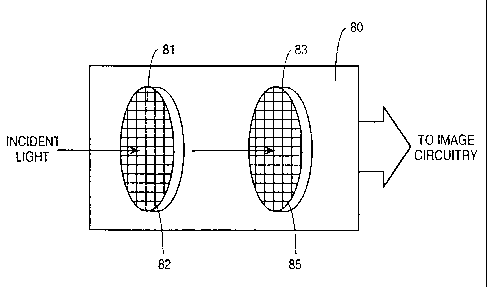
Figure 8 illustrates a CMOS image sensor in accordance with another
embodiment of the invention. The CMOS sensor 80 comprises a pixel array 83 and
a
phosphor layer 81. Photons that strike the pixel array 83 is first absorbed by
the
phosphor layer 81 and re-radiated in the infra-red wavelength where the image
sensor 80
6
WO 00/74140 CA 02373595 2001-11-16 PCT/US00/13718
can operate at optimal quantum efficiency. In this configuration, a color
filter array is
not used. The phosphor layer 81 comprises a plurality of phosphor dots 82,
each dot 82
corresponding to a pixel 85 in the pixel array 83. Each phosphor dot 8?
absorbs photons
of a particular wavelength in the visible spectrum and re-radiates photons of
a
wavelength in the infra-red spectrum. In this manner, the phosphor layer 81
performs
the color separation. Stated differently, the position of each phosphor that
absorbs a
particular wavelength (i.e., red, green or blue) in the phosphor layer
determines the RGB
pattern to be captured by the pixels in the pixel array. Because each phosphor
dot
absorbs only a wavelength and emits in the infra-red wavelength, a color
filter array is no
longer required.
One advantage of using a phosphor layer is that the time domain may be
adjusted
such that the phosphor absorbs photons and re-radiates at a longer period of
time. This
allows the pixels of the pixel array to be exposed to a particular image for a
longer period
of time. The sampling time of a CMOS sensor can be adjusted to accommodate for
the
extended time, allowing for fuller penetration of the incident photons into
the surface of
the pixel array.
Figure 9 illustrates a CMOS image sensor 90 in accordance with an embodiment
of the invention. In this embodiment, the image sensor 90 comprises an
isotropric
emissions reflector 91, a phosphor layer 93 and a pixel array 95. The role of
the
isotropic emissions reflector is as follows: Generally, incident light
entering the CMOS
image sensor has an infra-red wavelength component. The infra-red wavelength
component interferes with the RGB pattern generated by the pixel array 95 in
that the
infra-red wavelength photons converted by the phosphor layer 93 is
indistinguishable
from the infra-red wavelength component of the incident light.. The isotropic
emissions
reflector filters the infra-red wavelength component of the incident light by
reflecting it
away from the phosphor layer 93. Another role of the isotropic emissions
reflector 91 is
that the phosphor layer generally emits the converted infra-red wavelength
photons in
both directions, that is, towards the pixel array 95 and also towards the
isotropic
emissions relfector 91. The isotropic emissions reflector 91 reflects the
transmitted the
infra-red wavelength photons back into the phosphor layer 93. Isotropic
emissions
7
WO 00/74140 CA 02373595 2001-11-16 PCT/US00/13718
reflectors are commercially available, for example, from OCLI located in Santa
Rosa,
California.
Figure 10 illustrates an embodiment of a imaging system 100 in accordance with
the present invention. The imaging system 100 may be, for example, a camcorder
or a
digital camera or any system that is related to digital processing. As shown
in the figure,
an image sensor 101 including a phosphor layer in accordance with the
invention is
coupled to an imaging circuitry 103 that is further coupled to a memory device
105. The
memory device 105 may be semiconductor memories, magnetic disks or optical
disks
capable of storing images. The operation of the imaging system 100 is as
follows:
incident light containing an image falls on the image sensor 101 designed in
accordance
with the present invention. The image sensor 101 captures the image in a
manner as
described with respect to Figures 1 and 2. The charges generated by the pixels
are sent
to the imaging circuitry 103 for processing. The image represented by the
electrical
signals is processed by the imaging circuitry 103 and may be stored in the
memory
device 105 or transmitted out of the imaging system.
In the foregoing specification, the invention has been described with
reference to
specific embodiments thereof. It will, however, be evident that various
modifications
and changes can be made thereto without departing from the broader spirit and
scope of
the invention as set forth in the appended claims. The specification and
drawings are
accordingly, to be regarded in an illustrative rather than a restrictive
sense.
8