Note: Descriptions are shown in the official language in which they were submitted.
CA 02374006 2001-11-14
1
DESCRIPTION
OPTICAL WRITING HEAD AND METHOD OF CORRECTING
THE DEVIATION OF A LINE OF LIGHT SPOTS
TECHNICAL FIELD
The present invention relates to an optical writing head,
in particular to an optical writing head in which the
deviation of a line of light spots due to manufacturing
dispersion of a rod-lens array. The present invention
further relates to a method of correcting the deviation of a
line of light spots.
BACKGROUND ART
A writing head of an optical printer, i.e. an optical
writing head is a light source for exposing a photosensitive
drum and comprises a line of light-emitting points consisting
of a light-emitting element array. The structure of an
optical printer including an optical writing head is shown in
Fig. 1. An optically conductive material (photosensitive
material) such as amorphous Si is provided on the surface of
a cylindrical drum 2, which is rotated at the printing speed.
The surface of the photosensitive material is uniformly
charged with an electrostatic charger 4. Then, light
corresponding to a dot image being printed with an optical
writing head 6 is projected onto the surface of the
photosensitive material to neutralize the charge on the area
to which the light is projected. Next, a developer 8
deposits the toner on the photosensitive material surface in
accordance with the charged pattern on the photosensitive
material surface. The transfer unit 10 transfers the toner
CA 02374006 2001-11-14
2
on a paper sheet 14 fed from a cassette 12. The toner on the
paper sheet is thermally fixed by the heat applied by a fixer
16, and the paper is sent to a stacker 18. Upon completion
of transfer, on the other hand, the charge on the drum is
neutralized over the entire surface with an erasing lamp 20,
and the remaining toner is removed by a cleaner 22.
The construction of the optical print head 6 is shown in
Fig.2. This optical print head comprises a light-emitting
element array 24 and a rod-lens array 26, and the lens is
adapted so as to focus on the photosensitive drum 2. The
rod-lens array be composed of alternately stacked rod lenses,
for example.
The inventors of the present invention have interested
in a three-terminal light-emitting thyristor having a PNPN
structure as an element of the light-emitting element array,
and have already filed several patent applications (see
Japanese Patent Publication Nos. 1-238962, 2-14584, 2-92650,
and 2-92651.) These patent publications have disclosed that
a self-scanning function for light-emitting elements may be
implemented, and further have disclosed that such self-
scanning light-emitting element array has a simple and
compact structure for the light source of a printer, and has
smaller array pitch of thyristors.
The inventors have further provided a self-scanning
light-emitting element array having such structure that an
array of light-emitting thyristors having transfer function
is separated from an array of light-emitting thyristors
having writable function (see Japanese Patent Publication
No.2-263668.)
Referring to Fig.3, there is shown an equivalent circuit
CA 02374006 2001-11-14
3
diagram of a fundamental structure of this self-scanning
light-emitting element array (two-phase driving and cathode
common type). According to this structure, the light-
emitting element array comprises transfer elements T1, TZ, T3
~~~ and writable light-emitting elements L1, LZ, L, ~~~ , these
elements consisting of three-terminal light-emitting
thyristors. The structure of the portion of an array of
transfer elements includes diode D1, DZ, D3 w as means for
electrically connecting the gate electrodes of the
neighboring transfer elements to each other. Vex is a power
supply (normally 5 volts), and is connected to all of the
gate electrodes G1, G2, G, ~~~ of the transfer elements via a
load resistor RL, respectively. Respective gate electrodes
G1, GZ, G, ~~~ are correspondingly connected to the gate
electrodes of the writable light-emitting elements L1, L2, L3
~~. A start pulse ~5S is applied to the gate electrode of the
transfer element T1, transfer clock pulses ~ 1 and ~ 2 are
alternately applied to all of the anode electrodes of the
transfer elements, and a write signal ~I is applied to all
of the anode electrodes of the light-emitting elements.
The operation of this self-scanning light-emitting
device will now be described briefly. Assume that as the
transfer clock ~ 1 is driven to a high level, the transfer
element T2 is now turned on. At this time, the voltage of
the gate electrode GZ is dropped to a level near zero volt
from 5 volts. The effect of this voltage drop is transferred
to the gate electrodes G, via the diode D2 to cause the
voltage of the gate electrode G3 to set about 1 volt which is
a forward rise voltage (equal to the diffusion potential) of
the diode D2. On the other hand, the diode D1 is reverse-
CA 02374006 2001-11-14
4
biased so that the potential is not conducted to the gate G1,
then the potential of the gate electrode G1 remaining at 5
volts. The turn on voltage of the light-emitting thyristor
is approximated to a gate electrode potential + a diffusion
potential of PN junction (about 1 volt.) Therefore, if a
high level of a next transfer clock pulse ~ 2 is set to the
voltage larger than about 2 volts (which is required to turn-
on the transfer element T,) and smaller than about 4 volts
(which is required to turn on the transfer element TS), then
only the transfer element T3 is turned on and other transfer
elements remain off-state, respectively. As a result of
which, on-state is transferred from TZ to T,. In this manner,
on-state of transfer elements are sequentially transferred by
means of two-phase clock pulses.
The start pulse ASS works for starting the transfer
operation described above. When the start pulse ~ S is
driven to a low level ( about 0 volt ) and the trans fer clock
pulse ~2 is driven to a high level (about 2-4 volts) at the
same time, the transfer element T1 is turned on. Just after
that, the start pulse ~S is returned to a high level.
Assuming that the transfer element Tz is in the on-state,
the voltage of the gate electrode GZ is lowered to almost
zero volt. Consequently, if the voltage of the write signal
~ I is higher than the dif fusion potential ( about 1 volt ) of
the PN junction, the light-emitting element L2 may be turned
into an on-state (a light-emitting state.)
On the other hand, the voltage of the gate electrode G1
is about 5 volts, and the voltage of the gate electrode G3 is
about 1 volt. Consequently, the write voltage of the light-
emitting element L1 is about 6 volts, and the write voltage
CA 02374006 2001-11-14
of the light-emitting element L3 is about 2 volts. It
follows from this that the voltage of the write signal
which can write into only the light-emitting element LZ is in
a range of about 1-2 volts. When the light-emitting element
5 L2 is turned on, that is, in the light-emitting state, the
amount of light thereof is determined by the write signal
Accordingly, the light-emitting elements may emit light at
any desired amount of light. In order to transfer on-state
to the next element, it is necessary to first turn off the
element in on-state by temporarily dropping the voltage of
the write signal ~5= down to zero volts.
The self-scanning light-emitting element array described
above may be fabricated by arranging a plurality of light
emitting element array chips in one line so as to have a
desired number of light-emitting points.
In an optical writing head using such self-scanning
light-emitting element array, there is a problem in that a
line of light spots which are projected on the photosensitive
drum is deviated from a straight line in a sub-scanning
direction due to the manufacturing dispersion of a rod-lens
array. Fig.4 shows the condition where a line of light spots
is deviated in a sub-scanning direction. The light 41
emitted from each light-emitting point 40 of a straight-line
light-emitting element array 28 passes through a rod-lens
array 26 constructed by alternately stacked rod-lenses 27.
The light passed through the rod-lens array is projected onto
the photosensitive drum (not shown) to form a line of light
spots 42.
It is apparent from the figure that a line of light
spots deviates in a sub-scanning direction to draw a slightly
CA 02374006 2001-11-14
6
convex line. It is noted herein that the sub-scanning
direction is a direction perpendicular to an axis of rotation
of the drum. A main-scanning direction is that in parallel
with the axis of rotation of the photosensitive drum.
DISCLOSURE OF THE INVENTION
An object of the present invention is to provide an
optical writing head in which the deviation of a line of
light spots on the photosensitive drum in a sub-scanning
direction due to manufacturing dispersion of a rod-lens array
is corrected.
Another object of the present invention is to provide a
method of correcting a deviation of light spots due to
manufacturing dispersion of a rod-lens array.
According to the first aspect of the present invention,
an optical writing head is provided, which comprises .
a self-scanning light-emitting element array consisting
of a plurality of chips, each chip including
a self-scanning transfer element array having such a
structure that a plurality of three-terminal transfer
elements each having a control electrode for controlling
threshold voltage or current are arranged, the control
electrodes of the transfer elements neighbored to each other
are connected via first electrical means, a power supply line
is connected to the control electrodes via second electrical
means, clock lines are connected to one of two terminals
other than the control electrodes of each of the transfer
elements, and a start pulse line is connected to the control
electrode of the transfer element arranged at an end ; and a
light-emitting element array having such a structure that a
CA 02374006 2001-11-14
7
plurality of three-terminal light-emitting elements each
having a control electrode for controlling threshold voltage
or current are arranged, the control electrodes of the light-
emitting element are correspondingly connected to the control
electrodes of the transfer elements, and a line for applying
a write signal connected to one of two terminals other than
the control electrode of each of the light-emitting elements
is provided, and
a rod-lens array for projecting light emitted from the
self-scanning light-emitting element array onto a
lightsensitive drum to form a line of light spots,
wherein the timing of a start pulse supplied to the
start pulse line every chip is regulated to correct the
deviation of the line of light spots due to manufacturing
dispersion of the rod-lens.
According to the second aspect of the present invention,
an optical writing head is provided, which comprises .
a self-scanning light-emitting element array consisting
of a plurality of chips, each chip including
a self-scanning transfer element array having such a
structure that a plurality of three-terminal transfer
elements each having a control electrode for controlling
threshold voltage or current are arranged, the control
electrodes of the transfer elements neighbored to each other
are connected via first electrical means, a power supply line
is connected to the control electrodes via second electrical
means, clock lines are connected to one of two terminals
other than the control electrodes of each of the transfer
elements, and a start pulse line is connected to the control
electrode of the transfer element arranged at an end ; and a
CA 02374006 2001-11-14
light-emitting element array having such a structure that a
plurality of three-terminal light-emitting elements each
having a control electrode for controlling threshold voltage
or current are arranged, the control electrodes of the light-
s emitting element are correspondingly connected to the control
electrodes of the transfer elements, and a line for applying
a write signal connected to one of two terminals other than
the control electrode of each of the light-emitting elements
is provided, and
a rod-lens array for projecting light emitted from the
self-scanning light-emitting element array onto a
lightsensitive drum to form a line of light spots,
wherein the plurality of chips are divided into blocks
each consisting of a given number of chips, one start pulse
line is provided every block, and the timing of a start pulse
supplied to the one start pulse line is regulated every block
to correct the deviation of the line of light spots due to
manufacturing dispersion of the rod-lens.
BRIEF DESCRIPTION OF THE DRAWINGS
Fig.l is a schematic diagram of an optical printer
comprising an optical writing head.
Fig.2 is a schematic diagram of the structure of an
optical writing head.
Fig.3 is an equivalent circuit diagram of a self-
scanning light-emitting element array (two-phase driving,
cathode common type).
Fig.4 is a diagram showing the condition where a line of
light spots is deviated in a sub-scanning direction.
CA 02374006 2001-11-14
9
Fig.5 is a connection diagram of the chips in the
embodiment 1.
Fig.6 is a schematic diagram showing the condition of a
line of light spots on the photosensitive drum in the case
that the deviation of a line of light spots is not corrected.
Fig.7 is a timing diagram of each signal.
Fig.8 is a schematic diagram showing a line of light
spots projected on the drum after correction.
Fig.9 is a graph showing the experimental result
designating the effect of the correction for deviation of a
line of light spots in the embodiment 2.
BEST MODE FOR CARRYING OUT THE INVENTION
The embodiments of the present invention will now be
described with reference to the drawings.
Embodiment 1
An example of correction for the deviation of a line of
light spots in a self-scanning light-emitting element array
composed of five chips arranged in a straight line manner
will be illustrated. Fig.S shows a connection diagram of the
chips. In the figure, reference numerals 31, 32, 33, 34 and
35 designates first, second, third, fourth and fifth chips,
respectively. Each chip comprises 128 light-emitting points,
and " ~ " " ~ 1" " ~ 2" " ~ " and "V " written within each
S ~ ~ ~ I GR
chip designate pads for a start pulse ~S, clock pulses ~ 1
and ~ 2, a write signal ~ I and a power supply voltage VGx.
respectively.
Two-phase clock pulses ~ 1, ~ 2 and the power supply
voltage vGK are commonly applied to respective chips . Start
CA 02374006 2001-11-14
pulses X51, X52, X53, ~S4 and X55, and write signals ~5I1,
~ I2, ~ I3, ~ I4 and ~ I5 are in turn supplied to respective
chips.
Fig.6 shows the condition of a line of light spots on
5 the photosensitive drum in the case that the deviation of a
line of light spots is not corrected. An upper portion of the
figure shows the situation such that the light up condition
of each light-emitting point 40 of each chip is transferred.
An arrow "A" denotes a main-scanning direction, and an arrow
10 "B" a sub-scanning direction in the figure. A medium portion
of the figure shows a rod-lens array 26 consisting of rod-
lenses 27. A lower portion of the figure shows a line of
light spots 42 projected onto the drum.
As respective start pulses for the chips are supplied at
the same timing, a line of light spots is deviated in a sub
scanning direction due to the manufacturing dispersion of a
rod-lens array. In an example of Fig.6, a line of light
spots is deviated in such a manner that a slightly convex
line is drawn. The amplitude of this deviation is (6/128)X L
at maximum. "L" is herein a distance across which the
photosensitive drum rotates during the transfer operation
proceeds from the 1st light-emitting point to the 128th
light-emitting point.
Confirming the deviation of a line of light spots in a
sub-scanning direction, a data set for correction is formed
every chip. The generating timing of each start pulse is
shifted based on the data set to correct the deviation of a
line of light spots on the drum.
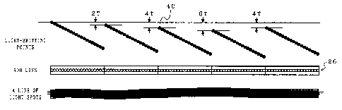
Fig.7 shows the start pulses each thereof is shifted in
generating timing. The numerals written in pulse waveforms
CA 02374006 2001-11-14
11
of each write signal in the figure designate numbers given to
each of 128 light-emitting points in each chip. "T" denotes
the time difference between the rise timings of the transfer
clock pulses ~S 1 and ~5 2, i.e. the period of light emission
of a light-emitting point. It is appreciated from the timing
diagram in Fig.6 that the start pulses X52, X53, ~S4 and X55
are delayed by 2T, 4T, 6T and 4T respectively with respect to
the start pulse X51.
Fig.8 shows the situation in which a line of light
spots is corrected using the start pulses shown in Fig.7. As
is shown in Fig.8, when the start pulse ~S1 supplied to the
first chip 31 is taken as a reference, the start pulse ~ S2
is supplied to the second chip 32 in a delay of 2T, the start
pulse ~ S3 to the third chip 33 in a delay of 4T, the start
pulse ~ S4 to the fourth chip 34 in a delay of 6T, and the
start pulse ~S5 to the fifth chip 35 in a delay of 4T. "T"
is herein the period of light emission of the light spots as
described above.
A line of light spots of each of the second, third,
fourth and fifth chips deviates downward by (2/128) X L,
(4/128)X L, (6/128) X L and (4/128)X L, respectively, assuming
that the photosensitive drum rotates upwardly in Fig.8. As a
result, the deviation of a line of light spots in a sub-
scanning direction may be corrected as shown in Fig.8.
According to the present embodiment, the correction for
the deviation of a line of light spots may be possible in a
( 1/64 ) X L unit by using common ~ 1 and ~ 2 clock pulses and
lighting up a light-emitting point shifted every chip.
Embodiment 2
CA 02374006 2001-11-14
12
The start pulse ~ S of each chip is independently
controlled, as shown in Fig.5, in the embodiment 1. However,
a plurality of chips in an optical writing head may be
divided into several blocks to control chips in a block by a
common start pulse
Considering now an optical writing head comprising a
self-scanning light-emitting element array consisting of, for
example, 56 chips, in which sinusoidal undulation having an
amplitude of at most 1 X L and about one period has been
caused in a line of light spots. In order to suppress the
amplitude of undulation of a line of light spots to (1/3)X L
or less for this optical writing head, 56 chips are divided
into 8 blocks, i.e. 7 chips per block to regulate the mean
value of deviation of lines of light spots in each block by
the timing of a common start pulse for each block. As a
result, the amplitude of dulation of a line of light spots
may be decreased to (1/3) X L or less. Referring to Fig.9,
there is shown a graph of the experimental result designating
the effect of the correction for deviation of a line of light
spots. Abscissa denotes a chip number, and ordinate the
deviation of light spots. It is recognized from the graph
that the amplitude of dulation of a line of light spots is
within ~ 0 . 5 X L .
While a cathode common type of self-scanning light
emitting element array is used in the optical writing heads
of the embodiments 1 and 2, an anode common type of self
scanning light-emitting element array may also be used.
Further, while two-phase transfer clock pulse is used, three
or more-phase clock pulse may also be used.
CA 02374006 2001-11-14
13
INDUSTRIAL APPLICABILITY
According to the present invention, it may be possible
to correct the deviation of a line of light spots on the
photosensitive drum in a sub-scanning direction. Therefore,
an optical writing head having a high printing quality may be
implemented.