Note: Descriptions are shown in the official language in which they were submitted.
CA 02374211 2001-12-20
WO 00/79595 PCT/GB00/02256
1
METHOD OF MODIFYING AN INTEGRATED CIRCUIT
The present invention relates to a method of modifying an integrated circuit,
in particular
through a series of scaling operations.
In particular, but not exclusively, the invention relates to a process by
which the physical
design or layout of an integrated circuit or subcircuit can be modified to
meet a different
set ofdesign and manufacturing rules. This method involves analysing data
ofthe existing
integrated circuit to determine the scaling factor then altering the shapes in
the original
by scaling the data, scaling individual layers, adjusting the edges of shapes
and swapping
geometries and cells through a defined sequence, according to a process
migration
technique.
Process migration is a technique for modifying integrated circuit designs so
that they can
be manufactured by new manufacturing processes with different geometric sizes
and
relationships. The physical size of an integrated circuits is limited by the
manufacturing
process used. The limiting factor is the size of the smallest component that
can be
produced, which at present is approximately 0.13 microns.
As new processes are devised, components can be manufactured to smaller sizes.
However, before an existing circuit can be built at a smaller scale using a
new
manufacturing process, the circuit layout must be re-designed. The overall
plan of the
circuit may be approximately the same, but different parts and components of
the circuit
may need to be scaled by differing factors. There are rules governing these
critical
dimensions. Some rely on manufacturing constraints, for example the smallest
feasible
size of a connection, whereas others depend on electronic factors such as
capacitance and
resistance.
When re-designed, computers can check the circuits for compliance with these
design
rules.
There may be various reasons for switching to a new manufacturing process,
including:
1 ) SPEED: smaller components have faster switching due to smaller charge
transfer
requirements and smaller signalling distances.
CA 02374211 2001-12-20
WO 00/79595 PCT/GB00/02256
2
2) SIZE: unit costs are lower, as more chips can be made per silicon wafer
3) ECONOMIC PRODUCTION: more products can be made on one production
line, allowing older, less economical, production lines to be closed.
The main problem is how to modify the physical design of the circuit. This can
be very
difficult and complicated.
Another reason for re-designing the chips is that many circuits are now
designed using
parts or components supplied by different manufacturers, called "system-on-
chip"
components. However, these components may be produced by different
manufacturers
and made to different design rules, and need to be re-designed so that they
all comply to
the same set of designs rules.
Reasons for re-designing might therefore include:
1 ) Compliance with particular design rules;
2) To make use of the latest manufacturing processes; and
3) To reduce the size of the component by a certain factor.
Existing methods of process migration are as follows:
Symbolic Migration. In this, each component, such as each transistor, is re-
generated
according to required technical specifications. The process is not very
successful,
especially for complicated circuits.
Compaction. It is known, for example from US 5640497, to provide a method of
redesigning layouts. In this method, the circuit is made smaller by squeezing
all the
dimensions to the smallest allowed by the design rules, first in the x
direction and then in
the y direction. The technique is partially successful, but "flattens" the
circuit: i.e. it
destroys the hierarchy of the building blocks. This requires huge computing
power to
achieve and, because the hierarchy can no longer be identified, it makes
subsequent
modification extremely difficult.
CA 02374211 2001-12-20
WO 00/79595 PCT/GB00/02256
3
Scaling. Scaling implies reducing the size of each component by a constant
factor. While
this reduces the size of the component, the resulting circuit will generally
be inoperable
as it is likely to break many hundreds-of thousands of design rules.
Therefore, while this
is sometimes seen as the ideal solution, it has not previously been
achievable.
It is an object of the present invention to provide a method of scaling an
integrated circuit
that mitigates at least some of the aforesaid problems.
According to the present invention there is provided a method of modifying an
integrated
circuit, the method including the steps of selecting a scaling factor, scaling
the circuit
according to the scaling factor, and adjusting the circuit for functionality
and design rule
compliance.
The method makes it possible to scale a circuit without losing functionality
or destroying
the hierarchy of the circuit.
Advantageously, the scaling factor is selected by calculating a plurality of
predetermined
scaling ratios and selecting a scaling factor that is equal to or greater than
the largest of
the predetermined scaling ratios. This ensures that the circuit is scaled to
the maximum
degree without violating essential design rules. Advantageously, the
predetermined
scaling ratios include the interconnect scaling ratio, the via size ratio and
the electrical
component geometry ratio.
Advantageously, the scaling factor is selected by rounding up to the next
whole grid point
from the largest of the predetermined scaling ratios. This ensures that the
components of
the circuit are placed correctly on the design grid.
Advantageously, the step of scaling the circuit according to the scaling
factor circuit
includes multiplying the co-ordinates of the circuit geometry by the scaling
factor.
Advantageously, the step of adjusting the circuit for functionality and design
rule
compliance includes a hierarchical layer scaling process. The hierarchical
layer scaling
process may include the step of scaling the components in a layer according to
a
predetermined layer scaling factor. This may be achieved by absolute scaling
(adding or
subtracting a fixed amount to the size of each component), or alternatively by
relative
CA 02374211 2001-12-20
WO 00/79595 PCT/GB00/02256
4
scaling (multiplying to increase or decrease the size of each component by a
fixed
percentage of its original size) . The hierarchical layer scaling process may
include the
step of scaling the components so as to maintain the connectivity of those
components.
The hierarchical layer scaling process may include the step of identifying
components that
meet predetermined width criteria, and scaling only components that do not
meet those
criteria. In this way, power connectors can be excluded from the scaling
process, to avoid
overheating problems.
Advantageously, the step of adjusting the circuit for functionality and design
rule
compliance includes a transistor edge adjustment process. The transistor edge
adjustment
process may include the step of adjusting the width of the polysilicon layer
and/or the
length of the diffusion layer. This restores the correct dimensions of the
components
making up the transistors, to ensure functionality.
Advantageously, the method includes the step ofupdating the contacts and vias.
The step
of updating the contacts and vial may include removing the existing contacts
and vias and
replacing them with new contacts and vial, to reduce current density.
Advantageously, the method includes the step of adding and/or deleting layers,
to
accommodate changes in technology.
Advantageously, the method includes the step of checking the circuit using a
layout
verification process to ensure compliance with design rules.
Advantageously, the method includes the preliminary step of analysing and
modifying the
circuit data, to reduce the time needed to complete the migration process.
Advantageously, the method includes the step of adding nodes containing design
parameters to devices in the circuit, so allowing easy access to information
about those
devices.
It is a further object of the present invention to provide a different process
migration
technique which may be described as "complex scaling" and which is applicable
to the
computer model of the layout of any existing integrated circuit. By using this
technique,
CA 02374211 2001-12-20
WO 00/79595 PCT/GB00/02256
the layout of a chip may be modified to be manufactured in any new process and
at any
scale that meets the new design rules.
The method is applicable to flat chip layouts and those containing design
hierarchy, which
may be defined as the placing of sub-cells into higher level circuits and
these, in turn,
5 being placed again. The hierarchy of the migrated chip matches the hierarchy
of the
original.
According to another aspect of the present invention, there is provided a
method of
scaling an integrated circuit comprising the steps of examining the existing
layout to
determine the amount by which the layout must be scaled, including determining
variable
geometry values; absolute geometry values; and a design grid, and carrying out
one or
more of gate width and length adjustment; layer scaling; polygon edge
adjustment; contact
replacement; adjust overlaps; addition or removal of layers; cell swapping;
and
verification.
An embodiment of the invention will be now be more particularly described by
way of
example and with reference to the accompanying drawings, in which:
Figure 1 shows circuit hierarchy where building blocks of circuitry are placed
into
larger blocks which can be placed again into yet larger blocks;
Figure 2 shows variable rule examples, where geometry must be equal to or
greater than a set distance and width;
Figure 3 shows fixed geometry value examples, where geometry dimensions must
equal a defined value;
Figure 4 shows interconnect spacing;
Figure 5 shows via geometries and arrays;
Figures 6a and 6b show CMOS transistor geometry, and Figure 6c shows spacing
considerations in a lateral transistor;
Figures 7a and 7b show general scaling;
Figure 8 shows CMOS transistor definition and transistor edge adjustment;
CA 02374211 2001-12-20
WO 00/79595 PCT/GB00/02256
6
Figure 9 shows adjusting the gate width of multiple transistors formed on a
single
diffusion geometry;
Figure 10 is illustrative of layer shrinking breaking connectivity;
Figure 11 illustrates hierarchical layer shrink with connectivity;
Figure 12 shows layer sizing by geometry width;
Figure 13 shows edge adjustment for transistors;
Figure 14 illustrates the use of contacts and vias to connect components of
the
circuit;
Figure 15 shows contact removal and replacement;
Figure 16 shows layer overlap;
Figure 17 shows a new well defined around an existing diffusion;
Figure 18 shows moving routing data between layers;
Figure 19 shows swapping new via cells for old;
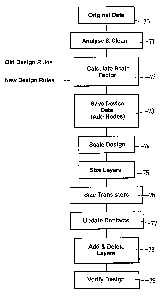
Figure 20 shows the steps of the migration process in the form of a flow
diagram;
Figure 21 shows the steps of the layer sizing process as a flow diagram;
Figures 22a, 22b and 22c show nodes placed over a transistor, a resistor and a
capacitor;
Figure 23 shows size calculations for a resistor, and
Figures 24a and 24b show size calculations for a capacitor.
A typical circuit hierarchy is shown in figure 1. Building blocks 1 of a
circuit are placed
into larger blocks 2, which can be placed again into yet larger blocks 3.
The cell migration process consists of three distinct steps:
1 ) Calculating the ideal scaling factor;
2) Scaling the entire circuit using the calculated factor; and
3) Fixing any errors in the circuit.
These steps are described in more detail below.
CA 02374211 2001-12-20
WO 00/79595 PCT/GB00/02256
7
In the first step, the ideal scaling factor is calculated using at least three
sets of equations,
which are described in more detail below with reference to figures 2 to 6.
When each of
these equations has been solved, the scaling factor used is the smallest
allowed by all of
the equations. In other words, the end circuit is no smaller than is allowed
by all of the
equations.
In the second step, the entire circuit is scaled using the calculated factor.
This is done by
multiplying every dimension by the same factor, which includes the positions
of the
building blocks, the positions and dimensions of the connectors, the positions
of
components within building blocks and the geometries of those components.
As shown in figure 7, the end result is a scale copy ofthe original circuit.
However, many
design rules will have been violated and component values will be incorrect:
e.g. the width
and length of the transistors may be too big or too small, giving either slow
operation or
non-operation. The resistors and capacitors may also have incorrect values.
The third step is to fix the errors. There are various steps to the fixing
operation, as
follows:
1 ) The size of all the geometries in any particular layer may be adjusted, by
adjusting
the layer size. For example, the co-ordinates ofthe shapes in the polysilicon
layer
may be adjusted. This is know as "layer sizing". For example, the area of
polysilicon over the di$usion making up the transistor may be increased or
decreased so as to achieve the minimum dimensions or to provide minimum
separations. This is shown in Figures 10-11. The dimensions are changed by a
fixed amount (e.g. 0.2 microns) rather than as a percentage of the original
shape.
2) Some parts of some components may be left unaltered: in particular power
connectors are not reduced in size, as this could affect the current flow in
the
circuit. The power connectors are identified by their size, as they are often
larger
than the other connectors, or by their signal name. The control logic
therefore
keeps components of a particular size unaltered, and reduces the size only
ofthose
that fall below a certain limit. This is shown in Figure 12.
3) Edge Adjustment. If the area of a component is too large, or if one edge is
too
close to another component following layer sizing or scaling, it can be
adjusted by
CA 02374211 2001-12-20
WO 00/79595 PCT/GB00/02256
8
moving one edge of the component rather than by changing the size of the whole
component. This is shown in Figure 13. For example, the size of a transistor
can
be altered in this way.
The scaling process therefore consists of three steps:
1 ) Overall scaling to a fixed factor;
2) Fixed scaling of components (layer scaling), which may include up to three
separate steps; and
3) Edge adjustment.
The process may in addition include the following features, which are
preferred but not
essential.
1 ) Contact removal and replacement (see Figure 15) it is desirable to provide
as
many electrical contacts as possible on each component, so reducing the
current
density through those contacts. Instead of re-scaling the contacts, it is
better
simply to remove them and then insert as many contacts as possible in the
space
available, according to the new design rules.
2) Adding and removing layers (see Figure 17). Some manufacturing processes
need
more layers than previous ones, and some do not require as many. The process
can be modified to add or subtract layers as required. For example, if the new
process requires an extra layer to make a transistor, the computer can be
arranged
to identify each transistor (for example by recognising a layer of polysilicon
over
a diffusion layer), and then add an extra layer as required.
The process and the steps making up the process will now be described in more
detail.
The technique for modifying the circuit involves a series of steps that scale
the data and
modify the shapes contained within it to comply with a set of design rules
that govern the
manufacturing process for production of the finished chip.
The techniques contained in this process will work for all components and
connection
geometries on a chip including, but not restricted to, MOSFET and bipolar
transistors,
resistors, capacitors and diodes.
CA 02374211 2001-12-20
WO 00/79595 PCT/GB00/02256
9
The input data for the process migration can be any existing chip or IC layout
or the
intellectual property contained therein, in an industry standard format such
as GDSII or
CIF. These files will contain the data that makes up the chip and may include
rectangles,
polygons, paths, instances, arrays and labels.
A modification sequence will include some or all of the following:-
Design analysis and scaling calculations;
General scaling;
Gate width and length adjustment;
Layer scaling;
Polygon edge adjustment;
Contact replacement;
Adjust overlaps;
Addition or removal of layers;
Cell swapping;
Verification.
In order to apply a factor to the general scaling calculations it is necessary
to examine the
existing layout to determine the amount by which the layout must be scaled.
There are
three factors that must be taken into account in this process:-
1. Variable geometry values;
2. Absolute geometry values;
3. The design grid.
Taking the first of these, namely variable geometry values, many of the design
rules in an
integrated circuit manufacturing process are given as a minimum value and must
be met
or exceeded when designing the circuit. An example of this would be a rule
that
determines the spacing between two geometries on the same layer that is
enforced to
ensure that the two geometries do not merge together during manufacture. The
spacing
rule may be exceeded as long as the minimum value given is not violated.
Examples of variable geometry values include widths, spacings and enclosures
of layers.
CA 02374211 2001-12-20
WO 00/79595 PCT/GB00/02256
Figure 2 shows variable rule examples, where the separation 4, the overlap 5
and the
width 6 of different geometries must be equal to or greater than a set
distance.
The second factor relates to absolute geometry values. Integrated circuit
design rules
usually have fixed values for certain geometries that must be met and cannot
be exceeded.
5 These are usually applied to contact and via holes that connect routing
circuitry and this
value must be met for each occurrence of these shapes. In addition, transistor
sizes are
defined in the circuit net list and this must be matched in the layout.
Failure to meet these
values will result in errors when checking the layout against the circuit
schematic or
netlist.
10 As shown in figure 3, examples of fixed values include contact and via
sizes 7, transistor
sizes 8, resistor sizes and capacitor sizes. Fixed geometry value examples are
shown,
where geometry dimensions must equal a defined value.
Finally, all integrated circuits are designed to have the co-ordinates of each
shape as a
multiple of a pre-defined grid. The scaling factor must take the new design
grid into
1 S account and this can be accomplished in two ways, by calculating the
scaling factor to
ensure that the co-ordinates of all shapes in the scaled layout fall on the
grid, or by
snapping co-ordinates to the grid as they are scaled. All co-ordinates in the
final chip
must be place on the defined design grid
The scale factor for any process migration will be calculated from the ratio
between the
rules in the new manufacturing process specification and the rules used for
the original
device. There are three distinct parts of a chip that can be the limiting
factor in scaling the
design and the ratio of each must be calculated. The largest of the three
ratios will be
defined as the limiting factor in scaling the chip.
1. Interconnect scaling ratio.
The width and spacing for each routing layer must be calculated as a ratio
defined by:-
Interconnect scaling ratio = (new width + new spacing) / (old width + old
spacing)
Figure 4 shows interconnect spacing 10 and width 11.
2. Via size ratio and enclosure.
CA 02374211 2001-12-20
WO 00/79595 PCT/GB00/02256
11
The via size is the size of the faced rectangles that make up the via holes
between routing
layers:-
Via size ratio = Max ((new via 1 / old via 1), (new via 2 / old via 2), ....)
Figure 5 shows a via geometry 12 that includes a first layer 13, a via 14 and
a second layer
15, and a 3x2 array 16 of via geometry.
3. Transistor geometry ratio.
The transistor geometry ratio is the relative shrink of the shapes that make
up the distance
between two transistors in separate pieces of diffusion:
Transistor geometry ratio = New (2a + 2b + 2c + 2d + a )/Old (2a + 2b + Zc +
2d + e)
Figures 6a and 6b show various CMOS transistor geometries, where L =
transistor length
and W = transistor width.
The maximum value derived from these calculations will determine the scaling
factor.
This scaling factor is rounded up to the next whole grid point, i.e. mod
(scale grid) = 0.
A fourth factor that may need consideration concerns circuits that contain
resistors and
capacitors. These need to be scaled depending on the values of the materials
used to
construct them in the two manufacturing processes. Resistors and capacitors
are defined
by the value per square unit of the materials used in their construction. The
ratio of these
values in the old and new manufacturing process is used to calculate the
scaling factor for
these circuit components. This is described in more detail below with
reference to Figs.
23 and 24.
Once the scaling factor has been determined, it is applied to each cell and
geometry in the
whole chip. Each co-ordinate is multiplied by the scaling factor to reduce the
chip in size
while keeping the geometries and hierarchy ofthe chip intact. At this stage,
the new chip
will be identical to the old in everything but scale.
The scaling of geometries and cells may be defined as coordinate scaling. Each
scalar
value is adjusted by:-.
(x co-ord * scale) (y co-ord * scale)
CA 02374211 2001-12-20
WO 00/79595 PCT/GB00/02256
12
Figures 7a and 7b show general scaling. In the general scaling process, the
original chip
18a is scaled down to create the new chip 18b, and each shape 19a,19b,19c in
the original
chip is replaced by a scaled down shape 20a,20b,20c. In each case, the new
dimensions
are equal to the old dimensions multiplied by the scaling factor. Each shape
within the
layout will be adjusted relative to the origin of the chip's axis, i.e. x = 0
y = 0.
The CMOS transistors in a circuit are determined by the overlap of two
materials, doped
silicon, known as diffusion, and polysilicon or occasionally metal. When
scaling the width
and length of a transistor, it is not always possible to apply an absolute
value to every
diffusion and polysilicon shape through the layout. Instead, the diffusion and
polysilicon
that make up the width and length of the transistor must change by a
percentage of the
transistor size and so each one must be scaled in turn and adjusted as a
multiple of its
current size. This involves the use of an edge adjusting method that
identifies the edges
of diffusion and polysilicon that make up each transistor's width and length
and moving
them to meet the required component value. Edge adjustment can be considered
as
distinct from scaling. Figure 8 shows a CMOS transistor definition and value
definition.
The individual transistors are identified with a Boolean operation that places
a marker
shape over any area where polysilicon 21 crosses diffusion 22. These shapes
will form the
basis for the rest of the transistor sizing operations in a circuit containing
CMOS
transistors.
The diffusion and polysilicon edges that make up the transistor are selected
and moved
by a percentage ofthe gate width or length to adjust the value of the
transistor. One piece
ofdi$usion may make up several transistors so the scaling routine must process
each edge
in turn to achieve the correct value for all of its transistors. Figures 8 and
9 show CMOS
transistor edge adjustment.
As shown in Fig. 8, the gate length L of a transistor can be altered by
adjusting the edges
23 of the polysilicon 21 forming the gate. The width W is adjusted by moving
the edges
24 of the diffusion 22 across the polysilicon 21. By adjusting these edges 23
and 24, the
parameters of the transistor can be altered, thus changing their effect on the
overall circuit.
CA 02374211 2001-12-20
WO 00/79595 PCT/GB00/02256
13
As shown in Fig. 9, many transistors may be constructed out of one piece of
diffusion
material 25, and adjusting the edges that make up one transistor may therefore
have an
effect on the others. By examining each edge on the diffusion, adjustments may
be made
that ensure all transistors meet required parameters. If necessary, an edge
making up
more than one transistor may be split to accommodate the required device
sizes. For
example, the edges 26 and 27 may be split at the points marked "X" to make the
changes
correctly.
Some manufacturing processes may require transistor sizes to change by a
differing
amount, depending on their original size or function in the circuit, so a
method of defining
them such as an equivalence table may be used to adjust the scaling process to
meet these
restrictions.
Once the entire layout has been scaled, each layer that makes up the design
must be grown
or shrunk to meet the design rules of the new manufacturing process. This is
achieved
with a technique called hierarchical layer scaling, which can grow or shrink
the shapes in
the circuit while maintaining connectivity between cells.
All of the shapes on a layer may be merged together with a Boolean function
before
scaling to remove excess overlaps between shapes and maintain connections
between
shapes on the same layer. In order to maintain the electrical integrity of the
circuit, the
connections between shapes on the various layers must be maintained, even
ifthese shapes
occur at a different level in the hierarchy. If they become separated, the
circuit will not
function so it is essential that the layer scaler takes this into account.
The problems of layer connectivity only occur when the layer in question is to
be shrunk
and the data contains hierarchy. By moving all of the edges of a shape
inwards, they will
detach from the shapes in sub-cells and this will break the electrical
connectivity in the
circuit.
Figure 10 is illustrative of layer shrinking breaking connectivity. The
circuit includes a top
cell 30 and a number of sub-cells 31 a,31 b,31 c. A shape 32a in the sub-cell
31 a abuts
shapes 32 in the top cell. If all the shapes 32a,32b,32c shrink they will
become detached
from each other, as shown in Fig. l Od.
CA 02374211 2001-12-20
WO 00/79595 PCT/GB00/02256
14
In order to remedy this, the shapes in the sub-cells are copied to the top
level and merged
with the data at that level before the shrink is applied. Once the shrinking
process is
complete, the shapes from the sub-cells are applied as a template to remove
any excess
material.
It is also possible to hold layer data to the edge of a cell which is defined
by the bounding
box of the cell's data or by a shape representing the boundary. Layout data
may be held
on the boundary of the cell to preserve scaling connectivity.
Figure 11 illustrates hierarchical layer shrink with connectivity. In the
example all three
shapes 32a,32b,32c shrink but they retain the connection between them. Only
the non-
connected edges are shrunk. Further rules may be applied to the layer scale to
restrict its
operation to shapes that match given size rules, i.e. they are less than or
greater than a
given dimension. This allows data on the same layer to be scaled by differing
amounts.
Figure 12 shows layer sizing by geometry width, the original shape 33a being
replaced by
the modified shape 33b. In this example, segments 34a,34b,34c of the shape can
be
shrunk if they meet size criteria. The shrunk segments 34a,34c stay attached
to the large
segment 35.
In order to meet all of the design rules for the migrated chip, it is
necessary to make
adjustments to parts of the shapes that make up the chip rather than the
shapes as a whole.
This can be described as "polygon edge adjustment", which examines each vertex
of a
shape and adjusts it according to its position relative to other shapes in the
layout.
The edges to be adjusted may be defined by the shapes on an individual layer
or identified
for modification by Boolean logic to define their function in the circuit.
Once this has
been determined, the edges can be adjusted by an absolute value from their
current
position or relative to another edge on the same or a different layer. They
may also be
adjusted by a percentage of their distance to another edge on the same or
different layer.
Figure 13 shows edge adjustment for transistors. It is possible to adjust a
first edge 36
that defines the transistor, or a second edge 37 for minimum overlap of
transistors or
contacts.
CA 02374211 2001-12-20
WO 00/79595 PCT/GB00/02256
Integrated circuit layouts use contact and via holes in dielectric layers to
allow routing
layers to connect the circuit's components. These are typically square shapes
with a size
and spacing defined in the technology's design rules. Connections between wide
tracks of
material require bigger contact areas. This may be defined by one big contact
or, more
5 usually, as an array of uniform contact shapes.
Contact and via shapes may be scaled as above. Alternatively, the existing
contacts and
vias may be removed and replaced with arrays of new shapes conforming to the
new
design rules. These may either be cells that make up the contact as a single
array of
shapes or a series of rectangles that cover the area to be connected. This
area is defined
10 through a sequence of Boolean functions that isolate the area to be
connected. The new
shapes conform to the new design rules by construction rather than scaling.
Contacts between other materials such as metal and polysilicon may be updated
using the
same techniques. As shown in Figs. 14a and 14b, contacts and vial 40 are used
to join
the silicon 41 in the components to the metal wires 42 that connect the
circuit. They are
15 also used to connect different layers of metal together to allow for
complex wiring. Most
integrated circuits will have multiple layers of wiring connecting the
components. These
contacts and vial are actually holes in the dielectric material 43 that
separates the different
layers from each other.
Contact shapes from metal to silicon are often created as simple polygons
rather than
instances and each of these is replaced with a new shape that meets the new
design rules.
Each contact is removed and replaced with a new shape that has the correct
dimensions.
In many cases, it is preferable to add as many contacts as possible between
layers to help
reduce current density through each contact. This can be achieved by
identifying the area
containing the contacts through a series of Boolean functions, and this area
can be filled
with as many contacts as will fit. For example, as shown in Figs 15a and 15b,
the two
large contact holes 44 of the old technology placed where the metal 42
overlaps the
silicon 41 can be replaced in the new technology by eight smaller contact
holes 45.
CA 02374211 2001-12-20
WO 00/79595 PCT/GB00/02256
16
Certain layers in an integrated circuit's layout are required to overlap other
layers by an
amount defined in the design rules. These layers are forced to comply with the
design
rules through Boolean logic or through edge adjustment as defined above.
Common examples of layer overlap include polysilicon overlap of gate and metal
overlap
of contact. Figure 16 shows layer overlap. The polysilicon 48 must overlap the
diffusion
49 by a minimum fixed distance 50.
Variations between integrated circuit manufacturing processes may mean that
some layers
in the original chip need to be removed and others added. Examples of this
would be
implant layers or isolation wells.
All shapes on superfluous layers are removed hierarchically, by identifying
each shape on
that layer and deleting it.
New layers may be defined in relation to an existing layer, possibly in
conjunction with
another layer: e.g. by placing a well around a diffusion layer, but only if it
is crossed by
polysilicon and makes a transistor. For example, figure 17a shows a diffusion
52 in a
transistor 53 and a diffusion 54 outside the transistor. As shown in figure
17b, a new
layer 55 in only added around the diffusion that is part of the transistor 53.
Data can also be promoted to new layers such as extra routing layers. Routing
information may be promoted from an existing layer up to a new layer. This
will allow
the layout to be compressed to take advantage of gaps created when these
shapes are
moved. Figures 18a and 18b show moving routing data between layers. In the old
arrangement shown in Fig. 18a, a first metal routing 56 is connected to a
second metal
routing 57 through a metall-metal2 via 58. In the new arrangement shown in
Fig. 18b,
routing information from a first metal routing 56 promoted to a third metal
routing 59 and
the vias 58a are changed accordingly.
Figures 19a and 19b show swapping new via cells for old. The via cell 60a
defined by the
old technology contains shapes for connecting two metal layers, first metal 61
and second
metal 62. This is swoped for a new via cell 60b containing shapes for
connecting the
metal layers in the new technology. Most vias are placed as instances of a sub-
cell that
CA 02374211 2001-12-20
WO 00/79595 PCT/GB00/02256
17
contains the three shapes that are used to construct it: two metal layers and
a via layer.
These can simply be replaced with a new via cell containing the same three
layers, or
re-sized to the new design rules. Some vias may be larger than minimum size
and have
multiple via holes connecting the two metal layers. When swapping these for a
new via
cell, the new cell is sized to match the number of via shapes in the old. By
swapping each
via cell in this way, the vias in the circuit are updated to meet the
constraints of a new
technology.
Once the entire circuit or a portion thereof has been migrated, it is verified
using industry
standard design tools. These will include a design rule checking (DRC) system
and a
layout-versus-schematic system (LVS). These will ensure that the newly
migrated chip
conforms to the new design rules and has retained the integrity of the
connections within
the circuit.
In addition, an interconnect timing analyser may be applied at any time to
check the layout
will perform correctly in the new manufacturing process. This may be applied
after
1 S general scaling as a rough guide to the circuit's performance in the new
process, even
though it does not conform to the new design rules. A more accurate simulation
will be
available once the migration process is complete.
When the layout migration is completed and the new chip has passed
verification, it may
be delivered in an industry standard format such as GDSII or CIF.
The steps of the migration process will now be described with reference to the
flow
diagram shown in Fig. 20.
The first step 70 is to input the original data. The original data is supplied
in an industry
standard format such as GDSII or CIF. The database will contain the shapes
that make
up the layout ofthe circuit and will include circuit elements such as
rectangles, polygons,
paths, instances, arrays and text. Connectivity information may also be
contained in the
database but the migration tools do not need this information to fimction.
The second step 71 is to analyse and clean the data. The time taken to migrate
the data
may be improved by modifying some of the data before starting the main
migration
CA 02374211 2001-12-20
WO 00/79595 PCT/GB00/02256
18
routines. This could include merging separate overlapping shapes or converting
interconnect elements from polygons to paths. Changes in the hierarchy of the
circuit may
also be useful such as converting individual shapes that make up a connection
between
layers to an instance of a connection cell.
While these techniques may improve the migration process, they are not
necessary to
complete the migration process.
The third step 72 is to calculate the scale factors. The scaling factor in a
process
migration will be determined by the ratios of the rules of the old
manufacturing process
and the rules in the new one. Examples of these rules are given above.
The fourth step 73 is to save the device data. Information contained in the
original
database may be referenced by programs throughout the migration process and so
it is
useful to be able to refer to this data easily. One technique, which is
described in more
detail below with reference to Fig. 22, is to add a node containing design
parameters to
each device in the layout. These nodes can be used to store information about
the devices
such as sizes or names of drawing layers.
The fifth step 74 is to scale the design. Once the scaling factor is decided,
each
co-ordinate in the design is multiplied by that scaling factor, giving a
design identical to
the original in everything by size.
The data for each element is scaled as follows:
Rectangle: Lower-left(X) * scale
Lower-left(Y) * scale
Upper-right(X) * scale
Upper-right(Y) * scale
Polygon: co-ordinates(X) * scale
co-ordinates(Y) * scale
Path: co-ordinates(X) * scale
CA 02374211 2001-12-20
WO 00/79595 PCT/GB00/02256
19
co-ordinates(Y) * scale
width * scale
Text: co-ordinate(X) * scale
co-ordinate(Y) * scale
font size * scale
Instance: co-ordinate(X) * scale
co-ordinate(Y) * scale
magnification * scale
Array: co-ordinate(X) * scale
co-ordinate(Y) * scale
magnification * scale
delta(X) * scale
delta(Y) * scale
The sixth step 75 is to size the layers. Once the data is scaled, each layer
may be sized to
meet the minimum width value defined in the design rules. This may be done to
ensure
that the data on each layers meets the rule for spacing and also has the
advantage of
reducing capacitance on each layer and improving circuit performance. Overall
scaling
calculations may take a subsequent adjustment in a layer's size into account
when deciding
on the primary scaling factor for the design.
Layers may be scaled by an absolute value or by a percentage of the layers
size. To scale
a layer by an absolute value, the following calculations are applied:
Rectangle: Lower-left(X) + value
Lower-le$(Y) + value
Upper-right(X) - value
Upper-right(Y) - value
CA 02374211 2001-12-20
WO 00/79595 PCT/GB00/02256
Polygon: co-ordinates(X) + or - scale'
co-ordinates(Y) + or - scale
Path: width * scale
5 'Addition or subtraction of the scale number will depend on the position of
the
co-ordinate on the hull of the shape. If it is on the a bottom or left edge of
the shape, the
scale number will be added to the co-ordinate, if it is on the top or right
edge of the shape,
it will be subtracted.
Relative scaling involves multiplying each co-ordinate in the shape by the
same scale
10 factor to adjust the co-ordinates.
The data for each element is scaled as follows:
Rectangle: Lower-left(X) * scale
Lower-left(Y) * scale
Upper-right(X) * scale
15 Upper-right(Y) * scale
Polygo~i: co-ordinates(X) * scale
co-ordinates(Y) * scale
20 Path: co-ordinates(X) * scale
co-ordinates(Y) * scale
width * scale
This technique will resize the shapes but it will also offset them from their
position relative
to the rest of the shapes in the circuit. In order to return them to their
original position,
the centre point of each shape can be calculated and the new shaped moved back
to the
central position of the old. The centre point is defined by taking the middle
of the
rectangular convex hull of the shape.
CA 02374211 2001-12-20
WO 00/79595 PCT/GB00/02256
21
The seventh step 76 is to size the CMOS transistors. The shapes that make up
the
transistors will be sized along with all of the other shapes in the layout
when general
scaling is performed. Further sizing may occur when individual layers are
scaled when
those layers are part of a transistor, i.e. diffusion or polysilicon. However,
transistors may
need to be scaled to account for other factors such as circuit timing and
driving
capabilities. The transistor scaling process is described in more detail above
with
reference to Figs. 8 and 9. In addition, the resistors and capacitors may also
be adjusted,
as described in more detail below with reference to Figs. 23 and 24.
The eighth step 77 is to update the contacts. This process is described in
more detail
above with reference to Fig. 15.
The ninth step 78 is to add and/or delete layers. Different manufacturing
technologies
may have a different number of layers making up the chip. Examples of this
include
implant and well layers.
These new layers are generated around existing layers and this can be achieved
by copying
each shape in the defining layers, oversizing it and then moving it onto the
new layer. Any
gaps between shapes on this new layer should be filled with the same material
if they are
found to be less than the specified minimum distance in the design rules.
Ifthe old layout contains shapes that are not required for the new
manufacturing process,
each of these shapes can be deleted from the database.
The tenth step 79 is to check the design. Once the migration process has been
completed,
the design can be checked using standard layout verification methods. These
include
design rule checking (DRC) and layout verses schematic checking (LVS). It may
also be
useful to perform a comparison between the old and new layouts (LVL). All of
these
checking techniques are considered standard in the electronics industry and
software to
perform these checks is available from a variety of vendors.
Transistors are adjusted by altering the dimensions of the shapes that are
used to construct
them. This is true for bipolar (NPN & PNP) devices and MOS (field effect)
devices.
Bipolar transistors can usually be considered as discrete components but MOS
devices
CA 02374211 2001-12-20
WO 00/79595 PCT/GB00/02256
22
will often be combined to save space in the circuit. The scaling calculations
for a bipolar
device will be governed by the rules that make up that device, which will
include minimum
widths, spacings, overlaps and enclosures.
The ratio of each of these rules in the old and new design rule specifications
must be
accounted for in the scaling calculations. The sizes for a CMOS transistor are
defined by
the common region of polysilicon overlapping diffusion. The width and length
of the
overlap defines the value ofthe transistor and adjusting the edges ofthe two
shapes alters
its value.
The layer scaling process will now be described in more detail with reference
to Fig. 21.
In order to meet the specifications of the new design rules, individual layers
may need to
be scaled up or down after general scaling is complete. This will ensure that
the data will
meet the requirements of the new manufacturing process and metal connection
layers are
reduced to their minimum width to reduce capacitance in the circuit. Layer
scaling is
most often applied to interconnection layers and the diffusion and polysilicon
layers that
1 S make up CMOS transistors.
The first step is to take the original data 81 and calculate the scaling
factor 82. The scale
factor for each layer is calculated after the general scaling factor has been
applied and can
be applied as an absolute value or as a percentage. These are calculated as:
Absolute value: (old layer width * general scale) - new layer width
2
Percentage value: new layer width
old layer width * general scale
The sizing value derived is taken from each side of a shape, hence the need to
divide the
value by 2.
It may be necessary to only alter the sizes of certain shapes while retaining
others as they
are. An example of this would be the wide power supply metal that is on the
same layer
as general interconnect shapes. In this case, only shapes that were narrower
than a certain
CA 02374211 2001-12-20
WO 00/79595 PCT/GB00/02256
23
value would be under or over sized. The process includes the steps of
selecting the shapes
83 that should be scaled and applying the scaling factor 84 to that selection.
When the polygon shapes on a layer are undersized, they will become detached
from each
other thus breaking the electrical integrity of the circuit. This must be
prevented to ensure
that the circuit still functions after the sizing procedure. This is further
complicated if the
shapes attach to other shapes at different levels of the circuit's hierarchy
as the problems
of attachment will depend on where the shapes are placed. If the shapes in
question are
oversized, they will still overlap each other so this problem will not arise.
The process
includes the steps of selecting the undersized shapes 85 and selecting from
those the
shapes for which it is necessary to retain connections 86.
One method of keeping all of the shapes within a cell connected is to merge
the shapes
together before sizing them. This means that no connected shapes are discrete
from each
other and so will not become detached through the sizing process.
Connections between shapes at different levels of the hierarchy can be
maintained by
copying the original shapes to a temporary layer before under-sizing the data
layer. Data
on each sub-cell can be under-sized in turn while leaving the outline of the
original in
place. When layer data in a cell touches the temporary layer in a sub-cell,
the connection
can be maintained using a sequence of Boolean operations to select connecting
shapes 87
and fill the gaps 88 between the top cell and sub-cell and maintain electrical
integrity.
Once the size value and connectivity information has been defined, the shapes
can be sized
by an absolute value 89 or a percentage 90, followed by offsetting the shapes
91, as
required.
A useful post processing function for layer sizing involves removing small
notches 92 and
bumps on each of the shapes on a layer that can be generated by the re-sizing
programs.
These should be removed as they are likely to result in errors being reported
at the design
rule checking stage.
A method for storing old design values in node properties will now be
described with
reference to Figs. 22a, 22b and 22c. Before the layout of the integrated
circuit is
CA 02374211 2001-12-20
WO 00/79595 PCT/GB00/02256
24
modified, it is useful to store the information about the current layout
through some
method for reference throughout the modification process. The information to
be stored
may include the sizes of the components that make up the circuit such as the
widths and
lengths of the transistors or the values of resistors and capacitors. By
storing this
information before modifying the design, subsequent modification routines can
check their
values against initial values without regard to how that data has been
ai~ected by the
scaling process.
One method of storing this data is to save it to an ASCII file and use this
for reference,
but this has the disadvantage of being divorced from the database containing
the layout
and needs to have detailed information on the location of each component,
making it
overly verbose.
A better method involves storing this information with each component in the
circuit.
Interrogating these components will return the information derived from the
original
circuit for comparison with the components' new values. For example, the
system may
add a simple "node" object to the database which carries the information for
the individual
component. These nodes are unaffected by the scaling process and can carry the
relevant
information as properties.
For example, Figs. 22a, 22b and 22c show respectively a node placed over a
CMOS
transistor containing the original W/L values, a node placed over a resistor
containing its
type, dimensions and value, and a node placed over a capacitor containing its
type,
dimensions and value.
The resistor calculations will now be described in more detail with reference
to Fig. 23.
Resistors are created by placing a piece of semi-conducting material between
two nodes.
The two factors that define a resistor's values are the resistance required
and the current
to be drawn_
The resistance value of a resistor is governed by the ratio of its width W to
its length L
and the "sheet resistivity" of the material from which it is made. In the
example shown
in Fig. 24, the resistor has the following values:
CA 02374211 2001-12-20
WO 00/79595 PCT/GB00/02256
P-diffusion resistor. Resistivity = 100 ohms per square.
Current density = 100 ~A per square.
Value = 8.5 squares @ 100 ohms/square = 850 ohms
Current = 0.5 squares * 100 ~A/square = 50 ~A
5 When applying the scaling factor to resistors, these ratios of the sheet
resistivity and
current density of the old and new resistor materials have to be taken into
account to
obtain the same value in the new resistors. As both the width and the length
of the
resistor will be equally affected, scaling a resistor will result in an
identical number of
squares and, therefore, an identical value. However, the sheet resistivity of
the new
10 process may be different and this will need to be taken in to account to
calculate its value.
This is achieved using the equation:
new number of squares = (old resistivity l new resistivity) * old number of
squares.
The width of the resistor after it has scaled will also affect the maximum
current that the
resistor can carry. The current involved will be dictated by the circuit
around the resistor
15 and so this value can only be obtained through examining circuit
performance. If the
resistor width needs to be increased to accommodate higher currents, the
length must be
scaled by an equal factor to maintain the same value of resistance.
The capacitor calculations will now be described in more detail with reference
to Figs. 24a
and 24b. Capacitors within an integrated circuit are formed by placing sheets
of
20 conducting or semi-conducting material 95,96 over one another with a third
material 97
between them forming a dielectric. The types of layers that may be used are
defined in
the design rules for each manufacturing process and these will also specify
the value of
the capacitors as a number of Farads per square. As Farads are such large
units, these will
typically be defined in pico-farads or femto-farads.
25 The value of the capacitor is given by:
width * length * nF per unit area
As the value of a capacitor is almost entirely defined by its surface area,
scaling a
capacitor will always alter this value. If this is the case, the dimensions of
the capacitor
will need to be adjusted after the scaling process is complete to retain the
value of the
capacitor.