Note: Descriptions are shown in the official language in which they were submitted.
CA 02374381 2001-12-21
WO 00/79681 PCTIUSOO/16191
LOAD CONTROL SYSTEM HAVING AN OVERLOAD PROTECTION CIRCUIT
FIELD OF THE INVENTION
The present invention relates generally to load control systems, and more
particularly, to a lighting control system having an overload protection
circuit to limit the
power dissipation of a switching element in the control system from exceeding
a
predetermined maximum level.
BACKGROUND OF THE INVENTION
Phase-controlled lighting controllers are well known and perform dimming
functions by selectively connecting an AC power source to a load during each
half-cycle. The
AC power may be switched using controllably conductive devices such as triacs,
anti-parallel
SCRs, field effect transistors (FETs) or insulated gate bipolar transistors
(IGBT). The amount
of dimming is determined by the ratio of "ON" time to "OFF" time of the
controllably
conductive device. In conventional forward phase-controlled dimming, the
controllably
conductive device (triac or SCR) is OFF at the beginning of each half-cycle
(i.e., at the zero
crossing) and turned ON later in the half-cycle. In reverse phase-controlled
dimming, the
controllably conductive device (FET or IGBT) is switched ON to supply power to
the load
at or near the zero crossing and is switched OFF later during the half-cycle.
For each method
of phase-controlled dimming, the ratio of ON time to OFF time is determined
based on a user-
selected desired intensity level.
Lighting controllers are rated to control a predetermined maximum load. If the
controller is overloaded the maximum temperature rating of the controllably
conductive
device may be exceeded and the device will not last as long as a properly
loaded device or fail
catastrophically rendering the controller useless. A lighting controller can
easily be
overloaded by an installer who connects too many lamps to the controller or by
a maintenance
person who replaces failed lamps with higher wattage lamps.
Another factor that may lead to an elevated device temperature is operating
the
lighting controller in an elevated ambient temperature. Lighting controllers
are rated to
operate in an ambient temperature range usually 0 to 40'C. An elevated ambient
temperature
would cause an otherwise properly loaded device to operate above its safe
operating
temperature.
CA 02374381 2001-12-21
WO 00/79681 PCT/US00/16191
-2-
Several methods of sensing overload conditions may be found in the prior art.
For example, U.S. Patent No. 5,325,258, to Choi et al., discloses a gate
driver circuit that uses
sense resistors to determine the current flowing through a low side and high
side FET. While
the FET is being driven (i.e., ON), a voltage across the sense resistor is
compared to a fixed
threshold voltage. If the voltage across the sense resistor remains above the
fixed threshold
for a period of time set by a blanking circuit, the FET is determined to be
overloaded and shut
down. The blanking circuit is provided to prevent spurious signals from
shutting down the
FET driver. While Choi et al. prevents overload conditions under certain
circumstances, it
would fail to detect a short circuit condition during the blanking period.
Also, because Choi
et al. compares the current passing through the FET to a fixed threshold, the
device may not
accurately detect overcurrent conditions that occur early in the ON period of
each half cycle.
U.S. Patent No. 5,010,293, to Ellersick, discloses a current limiting circuit
for
a power FET. A bipolar transistor is connected to shunt the gate of the power
FET to the
potential at its source when the bipolar transistor is conducting in order to
limit the current
passing through the power FET. A sense resistor is provided in series with a
conductor path
for controlling a base element of the bipolar transistor to cause the
transistor to conduct when
current through the sense resistor exceeds a predetermined amount. However,
the Ellersick
circuit is limited because it compares the current passing through the FET to
a fixed threshold,
which may not accurately detect overcurrent conditions early in the ON period
of each half
cycle and because the power FET becomes active to limit the current which
dissipates a lot
of power.
U.S. Patent No. 5,079,456, to Kotowski et al., discloses a current monitoring
circuit that includes a smaller sense FET that carries a current proportional
to a larger power
FET in the device. A comparator senses the voltage across the smaller
transistor to indicate
if the current in the sense transistor exceeds a predetermined amount equal to
a maximum
source current of the sense transistor. A second embodiment regulates the
source current
through the sense transistor in order to regulate the current through the
power transistor
wherein the sense transistor is operating in the linear region. By modifying
the drain to source
voltage of the sense transistor the device can regulate the current carried by
the power
transistor. A particular disadvantage of the Kotowski et al. system is that it
requires a separate
sense FET to monitor the power FET, which adds to the complexity and cost of
the
CA 02374381 2001-12-21
WO 00/79681 PCT/US00/16191
-3-
monitoring circuit. Again, the FET becomes active to limit the current which
dissipates a lot
of power.
U.S. Patent No. 4,937,697, to Edwards et al., discloses another protection
circuit that monitors instantaneous FET drain to source voltage to provide a
current sense
signal. When the current sense signal exceeds a predetermined reference limit
signal, a first
control circuit turns the FET OFF instantly. A reference generator provides a
reference limit
signal having a predetermined temperature variation as a function of the
sensed temperature
of the FET such that current limits may be set for low device temperatures. A
second control
circuit is provided to protect against overcurrent conditions created by short
circuits by turning
the FET OFF when sensed FET current exceeds a predetermined limit after a
delay. The
delay circuit inhibits operation of the control circuits until a predetermined
time after the FET
is turned ON. During this time there is no protection.
While each of the systems described above attempts to prevent overloading and
overheating of the controllably conductive devices for their particular
applications, they
require the use of more costly hardware or fail to provide adequate protection
over a wide
range of operating conditions and environments. In addition, the devices of
the prior art
function to limit the flow of current through the controllably conductive
device in overload
conditions by modifying the drain to source voltage, which does not reduce the
overall power
dissipation in the FET. The load control circuit of the present invention
reduces the current
flow to a safe operating level while not increasing dissipation in the FET.
The present
invention provides a solution to these problems.
SUMMARY OF THE INVENTION
In accordance with a first aspect of the present invention, there is provided
a
protection circuit for use in a load control system for limiting power
dissipated by an
electronic component that switches an AC source to a load. The electronic
component may
be, e.g., a field effect transistor. The protection circuit includes an
integrating circuit which
integrates a measured parameter of the electronic component over a
predetermined period of
time and produces an output value, a threshold generating circuit which
generates a first
threshold indicative of a maximum average power dissipation of the electronic
component,
and a comparator circuit which compares the first threshold and the output
value. The
CA 02374381 2001-12-21
WO 00/79681 PCTIUSOO/16191
-4-
comparator provides a signal to turn OFF the electronic component when the
output value
exceeds the first threshold.
In accordance with a feature of the invention, the first threshold may be
determined in accordance with an ON-state resistance of the electronic
component and the
measured parameter. Further, the first threshold may have a variable value
that changes
during one-half of a period of a fundamental frequency of the AC source. The
predetermined
period of time may begin when the AC source crosses a zero potential, and have
a length no
longer than one-half of a period of a fundamental frequency of the AC source.
According to other features of the invention, the protection circuit may
include
a reset circuit that holds OFF the integrating circuit during a period of time
that the electronic
component is normally OFF. A filtering circuit may be provided that receives
the signal from
the comparator circuit to smooth the control of the electronic component in
accordance with
a time constant of the filtering circuit. The protection circuit may further
include an error
generating circuit that receives an output of the filtering circuit and
compares the output of the
filtering circuit to a second threshold. The error generating circuit may turn
OFF the
electronic component based on the second threshold. The second threshold may
vary in
accordance with an ON-state resistance of the electronic component and the
maximum
average power dissipation of the electronic component. Further, the second
threshold may be
identical to the first threshold.
In accordance with another aspect of the present invention, there is provided
a load control system for delivering power from an AC source to a load. The
load control
system includes a zero cross detector that monitors the AC source having a
fundamental
frequency, at least one switching element that selectively connects the AC
source to the load,
a sensing circuit that senses an instantaneous ON-state parameter of the at
least one switching
element and produces an output, an overload circuit that determines if the at
least one
switching element is in an overload condition, a short circuit protection
circuit that also
receives the output to determine if the at least one switching element is
shorted, and a
controller that controls the load control system.
The controller of the load control system receives information from the zero
cross detector and outputs a gate drive signal to turn the at least one
switching element ON.
Also, the overload circuit receives the output and determines an integrated
value of the ON-
state parameter and compares the integrated value to a threshold indicative of
a maximum
CA 02374381 2001-12-21
WO 00/79681 PCTIUSOO/16191
-5-
average power dissipation of the at least one switching element to make its
determination if
the switching element is in an overloaded state, and reduces the ON time of
the at least one
switching element when the at least one switching element is determined to be
overloaded.
Further, the overload protection circuit may include the features of the above-
noted protection
circuit. The short circuit protection circuit also reduces the ON time of the
at least one
switching element when the at least one switching element is determined to be
shorted. The
OFF-state voltage of the at least one switching element may not be detected to
improve
accuracy of the overload circuit.
The load control system may be used to control capacitive loads, and in
particular may be used to control a lighting load. In such an environment, the
controller sets
an ON-time of the at least one switching element to a constant duty cycle for
a given intensity
level of the lighting load set by a user. Further, the overload conditions may
be visually
indicated to a user by flashing the lighting load.
According to features of the invention, the load control system may also
include a power supply that is connected to the AC source and outputs a
regulated voltage to
the controller. A gate drive circuit may be included that receives an output
of the overload
circuit and the short circuit protection circuit to turn OFF the at least one
switching element.
The gate drive circuit turns OFF the at least one switching element based on a
predetermined
prioritization, wherein the short circuit protection circuit has priority over
the overload circuit,
and the overload circuit has priority over the controller to turn OFF the at
least one switching
element.
In accordance with yet another aspect of the present invention, there is
provided a method of protecting a switching element connected between an AC
source and
a load from dissipating power in excess of a predetermined amount. The method
comprising
measuring a parameter of the switching element; integrating the measured
parameter over a
predetermined time period to produce an output; comparing the output to a
variable threshold;
producing a signal when the output exceeds the variable threshold; and turning
OFF the
switching element in response to the signal. The switching element may
comprise a field
effect transistor (FET), and the ON-state parameter may be a selected one of a
voltage across
the FET, a current through the FET, or a temperature of the FET.
According to features of the invention, the switching element may be turned
OFF when the instantaneous ON-state parameter exceeds a second threshold
value. Further,
CA 02374381 2001-12-21
WO 00/79681 PCT/US00/16191
-6-
a visual indication may be provided to a user that the switching element has
been overloaded
by, e.g., cycling power to the load by turning OFF and ON the switching
element.
Additional aspects and features of the present invention are detailed below.
BRIEF DESCRIPTION OF THE DRAWINGS
The foregoing summary, as well as the following detailed description of the
preferred embodiments, is better understood when read in conjunction with the
appended
drawings. For the purpose of illustrating the invention, there is shown in the
drawings an
embodiment that is presently preferred, in which like references numerals
represent similar
parts throughout the several views of the drawings, it being understood,
however, that the
invention is not limited to the specific methods and instrumentalities
disclosed. In the
drawings:
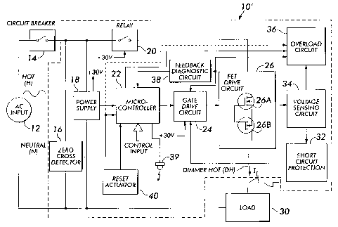
Fig. 1 is a block diagram of a load control circuit according to the prior
art;
Fig. 2 is a block diagram of a load control circuit having an overload
protection
circuit according to the present invention;
Fig. 3 is a graphical illustration of average power PAVG dissipated by a
controllably conductive device versus time for various load currents IL;
Fig. 4 is a graphical illustration of the average voltage VAVG across a
controllably conductive device versus time for various load currents. Also
illustrated are a
variable threshold and fixed threshold;
Fig. 5 is a graphical illustration of average power PAVG dissipated by a
controllably conductive device versus time for a controllably conductive
device operating at
various temperatures and having a constant load current IL;
Fig. 6 is a graphical illustration of the average voltage VAVG across a
controllably conductive device verus time at various operating temperatures
while controlling
a constant load current. Also illustrated are a variable threshold and fixed
threshold;
Fig. 7 is a block diagram of the overload circuit of Fig. 2; and
Fig. 8 is a schematic diagram of the overload circuit of Fig. 7.
DETAILED DESCRIPTION OF THE PREFERRED EMBODIMENT
Referring now to Fig. 1, there is illustrated a block diagram of a prior art 3-
wire
load control circuit 10 for controlling power to a load 30, such as a lighting
load. The load
CA 02374381 2009-06-30
.7.
control circuit 10 maybe part of an overall dimming system which allows a user
to selectively
set fighting levels within a room, building, etc. In the load control circuit
10, the load 30 that
is being controlled is an electronic low voltage transformer. Because this
type of load has a
capacitive input, it is typically controlled by a reverse-phase control
circuit such as the load
control circuit 10. Alternatively, the load 30 maybe a resistive load, such as
an incandescent
lighting load Examples of a reverse-phase control circuit may be found in U.S.
Patent Nos.
5,038,081 and 5,310,679, both to Maiale, Jr. at al. and commonly assigned to
the assignee of
the present invention The disclosures of the aforementioned U.S. Patents are
expressly
incorporated herein by reference in their eatirecies. It is noted that
magnetic or inductive
loads, which require forward-phase control, may not be controlled by the load
control circuit
10 as illustrated and de='bed below. However, with modifications to the gate
drive circuit
it is possible to generate a forward phase control signal to control these
loads. In addition, the
load control circuit 10 may be implemented in a 2-wire configuration by
connecting The zero
cross detector 16 and the power supply 18 reference to the lead marked "DI3".
T?re load control cit+cuit 10 is coupled to an AC input source 12 via a
circuit
breaker 14, which is provided to disconnect the AC source 12 if the load
control circuit 10
draws cutteat in excess of a predetermined maximum line current (e.g., 20
Amps) over a
predetermined period of time The predetermined period of time may be as long
as several
seconds or more which would prevent its use to protect the load control
circuit against short
circuits. Further, a single I OA load control circuit 10 may be the only
circuit connected to a
20A circuit breaker. The circuit breaker would not trip until the load current
exceeded 20A,
by this time the IOA load control circuit 10 may have suffered serious damage.
The c nil circuit 10 includes a zero anus detector 16 that monitors the AC
source voltage and outruns a signal when the instantaneous source voltage
passes through 0
V in either direction. Because the timing within the load control circuit 10
is based on
accurately determining when the AC source voltage passes through 0 V. the zero
cross
detector 16 may include a Bessel filter to remove unwanted noise from the AC
source voltage.
The filter allows the zero cross detector 16 to more accurately determine a
true zero crossing
of the fundamental frequency and also saves to reduce fluctuations in tinting
within the load
control circuit 10. An example of a lighting controller utilizing a Bessel
filter to more
accurately determine the true zero cross of the AC fimdamearai frequency may
be found in
pending U.S. Patent, No. 6,091,205 which is commonly assigned to the assignee
CA 02374381 2009-06-30
-8.
of the present invention.
A power supply 18 is provided to supply a regulated voltage (e.g., 30 V) and
a logic level voltage (e.g., SV) far components internal to the load control
circuit 10. The
S power supply 18 may include a switching device, such as a FET, to charge a
supply capacitor,
which allows the power supply 18 to be used over a wide range of AC source
voltages. The
regulated voltage may be supplied to drive a relay 20 or a gate drive circuit
24, whereas the
logic level voltage may be supplied to a microcoatroUcr 22 audits associated
support circuitry
(not shown).
A FET drive circuit 26 includes a pair of FETs 26A/26B arranged in a serves
configuration with a common source connection to switch the AC input source 12
to the load
30. The gates of both FETs 26A/26H are driven simultaneously by a signal from
a gate drive
circuit 24, which allows the control circuit 10 to use a voltage from power
supply 18 to turn
ON the FETs 26A/268. The FETs 26A/26B have the intrinsic characteristic of
being able to
conduct a load current IL of e.g.,16 A during the ON-sure; wbi a also being
able to withstand
the AC source voltage ofttte AC source 12 when in the OFF-sure: It is noted
that FETs are
used in the load control circuit 10 because tciace, which are used in standard
dimmers, cannot
be turned OFF in themiddle of the AC half-cycle without complicated control
electronics due
to trine Inching characteristics.
A voltage sensing circ uit 34 us provided to measure the us ON-state
voltage of the conducting FET 26A or 268 and outputs a signal indicative of
the ON-state
voltage of the conducting FET to a short circuit protection circuit 32. The ON-
state voltage
of the PET is indicative of the load cutest IL passing through the FET, and
when the FET is
operating in a safe region, the ON-state voltage is between approximately 2-4
V. The output
signal of the voltage sensing circuit 34 is monitored to prevent a
catastrophic failure of the
FET should a large currant pass theretbrough. In particular, the short circuit
protection circuit
32 senses if the signal from the voltage sensing circuit 34 has exceed a
predetermined level
indicative of a short circuit condition. The short circuit protection is
designed to be quick
acting. If the dimmer is turned an into a short circuit or very large
overload, the short circuit
protection instantly turns the FETs OFF before any serious damage to the PETS
can occur.
Because it is not necessary to detect the OFF sure voltage of the FET to
determine if that
has been a short circuit, the signal from the voltage sensing circuit 34 is
blocked when the
CA 02374381 2001-12-21
WO 00/79681 PCTIUSOO/16191
-9-
FETs are in the OFF-state. The signal is also blocked in the OFF-state because
the short
circuit protection circuit 32 monitors for a relatively low voltage,
therefore, it would be
difficult for the short circuit protection circuit 32 to accurately determine
a short circuit
condition if the OFF-state voltage was passed to the circuit 32, as the OFF-
state voltage of the
FET 26A or 26B may be as high as 400V.
A thermal cutout (TCO) 28 is provided to prevent the FETs 26A/26B from
reaching an unsafe operating temperature. The TCO 28 is selected so the FETs
turn off
completely or cut back their power to an a fixed level if the load control
circuit is overloaded
or operated in an elevated ambient environment. The TCO 28 is selected to
protect the FETs
26A/26B in case of a slight overload (up to -40%) over time. The TCO 28 has a
thermal lag
which prevents its use to protect against short circuits. Typically, the
thermal cutout 28 is a
fusible link that opens when heated to completely disconnect the AC input
source 12 from the
load 30. In the system of Fig. 1, the opening of TCO 28 signals to
microcontroller 22 to
disconnect load 30 from source 12 or cause it go to an extremely low light
level. The thermal
cutout 28 must be replaced by the user after opening to re-enable the load
control circuit 10.
Manual or automatically resettable TCOs can also be used. Proper placement of
the TCO 28
is very critical and presents difficulty in manufacturing.
The operation of the load control circuit 10 of Fig. 1 will now be discussed
with reference to the operation of the microcontroller 22. The microcontroller
22 receives
zero cross information from the zero cross detector 16 and serial data from a
SCI link (Control
Input) that includes, e.g., information related to a user-selected lighting
intensity level. The
zero cross information serves as a timing signal for driving the FETs 26A/26B
such that they
are alternately switched ON and OFF to connect the AC source 12 to the load
30. The
microcontroller 22 subtracts a phase shift that maybe created by the filter in
the zero cross
detector 16 to determine the appropriate timing for control of the FETs
26A/26B. Also, the
microcontroller 22 determines a period of time that each FET 26A/26B should be
in an ON-
state during its respective active half-cycle from the lighting intensity
level information in the
serial data.
Based on the above inputs, the microcontroller 22 outputs a gate drive signal
to the gate drive circuit 24, which in turn, drives FETs 26A/26B ON and OFF.
The
microcontroller 22 ensures that the conduction time of each FET 26A or 26B
creates a
constant duty cycle for a selected lighting intensity level. This also ensures
that the output
CA 02374381 2001-12-21
WO 00/79681 PCT/US00/16191
-10-
lighting level remains constant over a wide range of frequencies of the AC
source 12. The
power supply 18 for the gate drive circuit 24 is only charged on the negative
half-cycle
because this is the only half-cycle where a microcontroller common reference
and the FET
source common reference are the same.
As illustrated in Fig. 1, the gate drive circuit 24 combines the gate drive
signal
of the microcontroller 22 with the output of a short circuit protection
circuit 32. Because of
the rapid failure of the FETs that may occur under short-circuit conditions,
if the short circuit
protection circuit 32 determines that a short circuit may be present, the
short circuit protection
signal to the gate drive circuit 24 takes priority over the gate drive signal
from the
microcontroller 22 to immediately turn OFF the FETs 26A/26B. Under a short
circuit
condition, the gate drive 24 remains OFF until the next zero crossing. At that
point the FET
drive is reapplied until the short is detected again.
While the load control circuit 10 of Fig. 1 is adequate for most applications,
it is limited in that it does not gracefully control non-short circuit
overload situations. The
load control circuit 10 reacts to non-short circuit overload situations or
elevated ambient
temperature environments by cutting off the load current 'L via the thermal
cutout 28, which
must be reset or replaced. This approach is limited because load control
circuit 10 is typically
located in a location that is either inaccessible or distant from the actual
load 30 being
controlled. A further limitation is that it may lead to unsafe conditions in
the area being
illuminated because the lights (load) are turned OFF or to an extremely low
level that ensures
safe operation in overload conditions leaving an occupant in the dark. Also,
the elevated
ambient temperature condition may come and go with changing environmental
conditions
making trouble shooting difficult.
Referring now to Fig. 2, there is a block diagram of a load control circuit
10'
having an overload circuit 36 designed in accordance with the present
invention to overcome
the limitations of the prior art load control circuit. The present invention
improves upon the
prior art solution of thermal cutouts by employing an overload protection
device that limits
the maximum average power dissipation of the FETs to a predetermined level.
The overload
circuit 36 is designed to react slowly to overloads to reduce the ON-time of
an overloaded
FET to maintain the load current IL at a reduced level. In operation, this
feature of the present
invention advantageously maintains a reduced level of lighting from a level
that may be
requested by user input and does not completely cut off the lighting as in the
prior art.
CA 02374381 2001-12-21
WO 00/79681 PCTIUSOO/16191
-11-
The components of the load control circuit 10' that are similar to those of
Fig.
1 have similar reference numerals and, accordingly, will not be described
herein again. As
illustrated in Fig. 2, the output of the voltage sensing circuit 34 of the
load control circuit 10'
is provided to both the short circuit protection circuit 32 and the overload
circuit 36. The
overload circuit 36 receives the output of the voltage sensing circuit 34 and
integrates it over
each AC half-cycle to determine an average voltage VAVG across the FET over
time. At every
zero crossing the overload circuit 36 is reset in accordance with a signal
provided by the
microcontroller 22. Alternatively, the output of the zero crossing detector 16
may be used to
reset the overload circuit 36 (shown in dashed lines).
An overload is detected by overload circuit 36 when the integrated value
(i.e.,
an average voltage across the FET over time) exceeds a predetermined
threshold. Upon
detecting an overload, the overload circuit 36 outputs a signal to the gate
drive circuit 24 and
a feedback diagnostic circuit 38. The signal from the overload circuit 36
causes the gate drive
circuit 24 to turn OFF the conducting FET 26A or 26B so as to reduce the ON-
time, thus
decreasing both the power dissipation and temperature of the FET into a safe
operating region.
When the feedback diagnostic circuit 38 receives the signal from the overload
circuit 36, a
feedback signal is generated and output to the microcontroller 22. Upon
receiving the
feedback signal, the microcontroller 22 sets a register such that a visual
indication will be
provided to the user that an overload condition has occurred. The visual
indication may be
provided to the user by flashing alight emitting diode (LED) 39 on a module
contained within
the load control circuit 10, or by having the output of the FET 26A or 26B
cause the load 30
(e.g., lighting load 30) to cycle ON and OFF for a period of time, preferably
when the load
is initially turned either ON or OFF. It is preferable to provide such a
visual indication so
that the user is aware that the output of the load control circuit (dimmer)
has been reduced due
25 to an overload rather than a malfunction of the dimmer, and so that
corrective action may be
taken. The microcontroller 22 can be programmed so that the visual indication
continues to
alert the user even after an overload has been removed. A reset actuator 40
can be added to
the load control circuit 10' to return the system to a normal operating mode.
The reset
actuator 40 can be actuated by a factory trained representative after the
system has be
30 thoroughly checked out.
It is preferable to prioritize the signals from the short circuit protection
circuit
32, the overload circuit 36, and the microcontroller 22 that are received by
the gate drive
CA 02374381 2001-12-21
WO 00/79681 PCT/US00/16191
-12-
circuit 24. The highest priority is given to the short circuit protection
circuit 32 for the
reasons noted above with regard to Fig. 1. Although the slower reacting
overload circuit 36
protects against overcurrent and over-temperature conditions, the short
circuit protection
circuit 32 is needed to respond instantly to remove current from the FET if
the ON-state
voltage exceeds a safe operating point. The signal sent by the overload
circuit 36 to the gate
drive circuit 24 to turn OFF the FETs has a secondary priority to control the
FETs. A lower
priority is given to the microcontroller 22 gate drive signal, which serves to
control the FETs
when no faults are detected. Thus, the combination of the overload circuit 36
and the short
circuit protection circuit 32 provides awide range ofprotection in all
operating environments.
As noted above, an overcurrent condition is detected by overload circuit 36
when the integrated value of the voltage across the FET exceeds a
predetermined threshold.
This average voltage-based determination is made based on the following
relationships. The
power dissipation of the FET may be determined by the relationship:
P=Vy
R =I2*R
wherein V is the ON-state voltage across the FET, R is the ON-state resistance
RDS ON of the
FET, and I is the load current IL. While RDS ON is a known parameter that is
determined by the
intrinsic characteristics of the FET, determining the V2 and 12 terms requires
complicated
circuitry.
The present invention advantageously eliminates the need to utilize
complicated circuitry to determine the squared terms to calculate the power
dissipation of the
FET. In accordance with the present invention, the power dissipation of the
FET (PAVG) is
determined by comparing the average voltage VAVG across the FET to a variable
threshold VTx
(VAR) determined based on the ON-state resistance RDS ON of the FET and
maximum power
dissipation of the controllably conductive device. The variable threshold VTH
(VAR) also
accounts for the V2 term in determining power dissipated, therefore, the power
dissipation of
the FET may be determined quickly using less complicated circuitry.
The variable threshold VTH(VAR) of the present invention and its relationship
to
average power PAVG, load current IL, and average voltage VAVG across the FET
over a half-
cycle will now be described with reference to Figs. 3-6. Circuitry to
implement the
relationships is illustrated in Figs. 7 and 8, and will be described in detail
below. As noted
above, the variable threshold VTH(VAR) of the present invention is determined
based on the ON-
CA 02374381 2001-12-21
WO 00/79681 PCT/USO0/16191
-13-
state resistance RDS ON of the FET, and in addition, the maximum power
dissipation allowed
to maintain safe device operation for the thermal system being used.
Therefore, the variable
threshold VTH(vAR) can be advantageously "tuned" to aparticular FET within the
control circuit
10' for all combinations of conduction time, overload currents and
temperatures. In the
preferred embodiment, the FET is capable of dissipating 16 Watts in a maximum
ambient
temperature of 40'C. The load control circuit 10' of the preferred embodiment
is rated at 1 OA
with the overload circuit 36 starting to cut back the ON-time of the FET
26A/26B at around
a load current IL of 11.3A.
Lines 52, 54 and 56, respectively, of Fig. 3 illustrates the relationship of
power
dissipation PAVG versus time t for load currents IL of 16 A, 13 A and 11 A
over a half-cycle
at a fixed ambient temperature (40 C). A half-cycle of a 60 Hz AC signal has a
duration of
approximately 8.333 msec. As illustrated by the relationship of Fig. 3, if,
for example, it is
desired to limit maximum power dissipation of the FET to 16 Watts, then the
FET must be
turned OFF 4 msec into the half-cycle for a load current IL of 16 A, and
turned OFF 5 msec
into the half-cycle for a load current IL of 13 A. A load current IL of 11 A
does not exceed a
power dissipation of 16 W under the conditions presented.
Referring now to Fig. 4, there is illustrated the relationship of average
voltage
(VAVG) across the FET versus time, a variable threshold VTH(VAR), and a fixed
threshold
VTx (CONSTANT). The average voltage VAVG across the FET versus time for load
currents IL of
16, 13 and 11 A is illustrated by lines 58, 60 and 62, respectively and the
variable threshold
VTH (VAR) is indicated by line 64. The fixed threshold VTH (CONSTANT) is
indicated by line 66.
The variable threshold VTH (VAR) 64 is empirically derived so as to limit the
maximum power
dissipation to a fixed level (e.g., 16 W).
As noted above, the present invention compares the average voltage (VAVG)
across the FET to the variable threshold to determine if the FET is
dissipating too much
power, and thus is overloaded. This feature is illustrated in Fig. 4, wherein
line 64,
representing the variable threshold VTH(VAR), intersects line 58, representing
a load current IL
of 16 A, at approximately 4 msec into the half-cycle. As noted with respect to
Fig. 3, in order
to limit maximum power dissipation of the FET to 16 W, the FET must be turned
OFF 4 msec
into the half-cycle for a load current IL of 16 A. Likewise, the variable
threshold VTH (VAR)
intersects line 60, representing an IL of 13 A, at approximately 5 msec into
the half-cycle.
Again, as noted with respect to Fig. 3, in order to limit maximum power
dissipation of the
CA 02374381 2001-12-21
WO 00/79681 PCT/US00/16191
-14-
FET to 16 W, the FET must be turned OFF 5 msec into the half-cycle a load
current IL of 13
A. Finally, the variable threshold VTH (VAR) (line 64) does not intersect line
62, which
represents an IL of 11 A.
Therefore, as illustrated in Fig. 4, by comparing an average voltage across
the
FET to a variable threshold, a determination of power dissipation over a range
of load currents
can be made to limit a maximum power dissipation of the FET and provide
superior overload
protection. Further, as is evident from Fig. 4, the fixed threshold (line 66)
will not provide
adequate overload protection over a wide range of load currents. If the value
of VTH(CONSTANT)
is set to allow a 10 A current to flow, then for example, if the FET is
conducting a load current
IL of 16 A, the FET will not be turned OFF until 5.5 msec into the half-cycle.
Referring to
Fig. 3, at 5.5 msec into the half-cycle, the FET will be dissipating well in
excess of 20 W.
Thus, the fixed threshold will not provide a sufficiently low threshold early
in the half-cycle
to prevent an overload in the FET.
Fig. 5 illustrates how the temperature dependencies of the ON-state resistance
RDS ON of the FET may affect power dissipation. For example, in the present
invention, the
preferred FET is an STY34NB50, manufactured by SGS Thompson. The ON-state
resistance
of that FET at 25 C is approximately 0.11 to 0.13 Ohms when the load current
II, is 17 Amps.
At 130 C, the ON-state resistance of the FET is 2.25 times greater than at 25
C, or 0.25 to
0.29 Ohms. It is noted that to ensure a safe operating range, it is preferable
to use the worst
case ON-state resistance of 0.29 Ohms as the value of RDS ON-
Lines 68, 70 and 72 in the graph of Fig. 5 represent a load current IL of 11 A
at temperatures of 140 C, 120 C and 100 C, respectively. If, for example, it
is desired to
limit maximum power (PAVG) dissipation of the FET to 16 W, then the FET must
be turned
OFF at approximately 5.3 msec into the half-cycle when operating at a
temperature of 140 C,
and turned OFF at approximately 6 msec into the half-cycle when operating at a
temperature
of 120 C. An operating temperature of 100 C would not exceed a power
dissipation of 16
W with a load current of 11 A in the present example.
Fig. 6 illustrates the relationship of average voltage across the FET (VAVG)
versus time t. Lines 78, 76 and 74, respectively illustrate the average
voltage VAVG across the
FET for a load current IL 11 A at operating temperatures of 140'C, 1200C and
100'C,
respectively. Line 64 represents the variable threshold VTH (VAR), and line 66
represents the
fixed threshold VTH(CONSTANT)-
CA 02374381 2001-12-21
WO 00/79681 PCT/US00/16191
-15-
The variable threshold VTH (VAR) feature of the present invention may also be
used to limit power dissipation of the FET by accounting for the temperature
dependencies
of RDS ON. This feature is illustrated in Fig. 6, wherein line 64,
representing the variable
threshold VTH (VAR) intersects line 78, representing an operating temperature
of 140 C, at
approximately 4.75 msec into the half-cycle. As noted with respect to Fig. 5,
to limit
maximum power dissipation to 16 W, the FET must be turned OFF at approximately
5.3 msec
into the half-cycle for an operating temperature of 140 C. As can be seen, if
the same
variable threshold VTH (VAR) is used to check for an elevated ambient, the
system will slightly
over correct. This is because the contribution of ON-state resistance RDS ON
to power is not
squared, therefore over correction of the cutback time results. This allows
the FET 26A/26B
to cool and ultimately settle to a higher ON-time than is shown in Fig. 6. In
the example
shown, the load control circuit will start to cutback the ON-time to
approximately 4.75 msec
instead of 5.3 msec. The load control circuit will settle at a value between
these two times
because as the power is cut back by reducing the "on" time, the device will
run cooler because
both the IL and the ON-state resistance RDS oN will decrease. Similarly, the
variable threshold
VTll(VAR) intersects line 76, representing an operating temperature of 120'C,
at approximately
5.3 msec into the half-cycle. Again, as noted with respect to Fig. 5, to limit
maximum power
dissipation to 16 W, the FET must be turned OFF at approximately 6 msec into
the half-cycle
for an operating temperature of 120 C. Finally, the variable threshold does
not intersect line
74, which represents a temperature of 100 C.
Therefore, the variable threshold of the present invention may be used to
account for a wide range of operating temperatures and variations in load
current IL to
accurately limit maximum power dissipation the FET. As shown in Fig. 6, a
fixed threshold
(line 66) will not provide adequate protection against thermal effects. For
example, a FET
operating at 140'C will not be turned OFF until 6.3 msec into the half-cycle,
which translates
to a power dissipation of approximately 18 W. Thus, the fixed threshold will
not provide a
sufficiently low threshold early in the half-cycle to prevent an overload in
the FET.
As illustrated by Figs. 3-6, a comparison of an average voltage across the FET
to a variable threshold, as determined in accordance with the present
invention, prevents
overloads over a wide range of operating conditions.
An exemplary overload circuit 36 implementing the relationships described in
Figs 3-6 will now be described in greater detail with reference to Figs. 7 and
8. Fig. 7
CA 02374381 2001-12-21
WO 00/79681 PCTIUSOO/16191
-16-
illustrates a block diagram of the overload circuit 36, whereas Fig. 8
illustrates a schematic
diagram of the presently preferred embodiment. As illustrated, the overload
circuit 36
includes an integrator 40, an integrator reset 48, a threshold detector 42, a
low pass filter 44,
a cutback error generator 46, and a ramp generator 50.
The integrator circuit 40 receives the output of the voltage sensing circuit
34,
which as noted-above, provides an indication of the instantaneous ON-state
voltage of the
FET 26A or 26B. The integrator 40 determines the average voltage VAVG across
the FET.
The average voltage is proportional to the Volt-Seconds that build-up across
the FET in its
ON-state during a half-cycle of the AC waveform. The VAVG output of the
integrator 40 is
variable and will vary with FET temperature, ON-state resistance RDS ON, and
the load current.
The integrator 40 output is reset at the beginning of each AC half-cycle by an
integrator reset 48 to ensure that only the present half-cycle information is
being measured.
The microcontroller 22 provides the reset pulse via the gate drive circuit 24
to clear the
integrator 40 based on an output of the zero cross detection circuit 16.
Alternatively, a signal
may be sent directly from the zero cross detection circuit 16 to the
integrator reset 48. The
integrator reset 48 functions to hold off (reset) the integrator 40 during the
period of time that
the FETs are OFF. It is preferable to reset the integrator 40 because the OFF-
state voltage of
the FET is very large compared to the ON-state voltage, and in order to
monitor a relatively
low ON-state voltage of the FET, the OFF-state information should be removed
from the
integrator 40. Further, the OFF-state voltage is not useful in determining an
overload
condition of the FET.
The threshold detector 42 compares the output of the integrator 40 (VAVG) to
the variable threshold VTH (VAR) in order to provide an indication that the
FET is overloaded
by dissipating too much power, conducting too high a load current IL, or if
the FET is reaching
an unsafe operating temperature. As noted above, the variable threshold VTH
(VAR) is
empirically determined as described above.
A ramp generator 50 is provided to generate the variable threshold VTH(VAR) in
accordance with the above. The variable threshold, as describe above, is a
ramping value and
is used to reduce the ON-time of the FET to maintain a constant maximum power
dissipation
in the FET over a wide range of overload conditions. That is, the slope and
amplitude of the
ramp generator is chosen to maintain the desired constant power dissipation in
the FET for
all combinations of conduction times, overload currents, and elevated ambient
conditions.
CA 02374381 2001-12-21
WO 00/79681 PCTIUSOO/16191
-17-
The ramp generator 50 provides the ramping waveforms to both threshold
detector 42 and an
cutback error generator 46 (described below). The ramping waveform is reset at
the AC
source zero crossing, as indicated by the microcontroller 22. In a preferred
embodiment, the
ideal variable threshold VTH (VAR) is approximated by an RC circuit to be
described below.
The output of the threshold detector 42 is filtered by a low pass filter 44
having
a long time constant (e.g., greater than one second) to provide a measure of
additional stability
in the operation of the load control circuit 10'. The low pass filtering
provides hysteresis to
help prevent the cutback error generator 46 from causing an over-correction,
which could
cause visible fluctuations in the light output from the load. To help prevent
over-correction,
the low pass filter 44 smooths the output from the threshold detector 42. The
time constant
of the low pass filter is preferably approximately 1-2 sec. This time constant
is short enough
to prevent the FET from reaching unsafe temperatures during overloads before
the conduction
time is reduced. However, this slow response makes the overload circuit 36
ineffective in
providing a quick shutdown during a large overload or short circuit. Because
of this
hysteresis the short circuit protection circuit 32 is used in addition to the
overload circuit to
provide complete protection.
The cutback error generator 46 receives the filtered signal from the low pass
filter 44 and compares the filtered signal value to another ramping signal
from the ramp
generator 50 which is reset at each AC line voltage zero crossing. The ramping
signal is used
to determine how much the FET conduction time (ON-time) is reduced for a
particular amount
of Volt-Seconds measured across the FET by the integrator 40. The cutback
error generator
output is derived from the intersection of the level of heavily filtered DC
voltage from the low
pass filter 44 with the ramp to generate the proper "cutback" signal. The
"cutback" signal
ensures the FET ON-time will be the correct value to limit the FET power to 16
W. The
output of the cutback error generator 46 is a square wave which is provided to
the gate drive
circuit 24 to shut OFF the FETs during a half-cycle if an overload condition
occurs. The
output is also provided to the feedback diagnostic circuit 38 so information
may be provided
to the microcontroller 22 that the FET ON-time has been "cutback" from the ON-
time being
called for by the microcontroller 22 based on user input. The microcontroller
22 can then
optionally indicate the overload or over-temperature to the user.
Referring now to Fig. 8, there is illustrated an exemplary schematic diagram
that corresponds to the functional blocks shown in Fig.7. The voltage across
the FETs
CA 02374381 2001-12-21
WO 00/79681 PCTIUSOO/16191
-18-
26A/26B (Ql/ Q2) measured by the voltage sensing circuit 34 is input to the
integrator 40 by
having the voltage on R21 and R20 pulled low during the FET on time. When the
FET is off
the diodes (Dl and D2) are reversed biased and the voltage is held at 12 V by
the supply 18.
This ensures the input the integrator 40 will not be over driven above the
supply when the
FETs are OFF.
The integrator 40 consists of R22 and C2, which provide a time constant that
allows the capacitor to charge to a level near l Volt through the half cycle
with the FET
carrying 10 A of load current. The capacitor is reset to zero volts whenever
the gate drive to
the FETs is pulled low. This is accomplished by the input of the comparator
being pulled
below a threshold level half way between the supply rail and common.
The threshold detector 42 receives the voltage from the integrator capacitor
C2
and compares it to a ramp function from the ramp generator 50. The output of
this comparator
goes low whenever the integrated voltage exceeds the ramp. The output will
stay low until
the capacitor is reset as described above.
The FET gate drive circuit 24 must not change immediately when the
integrator 40 exceeds the ramp because the amount of reduction of the FET
conduction time
will cause the FET to cool and lower the integrator voltage further. The
result of this is an
over correction and the output voltage to the load will fluctuate. To avoid
this a low pass filter
44 is used average the error from the threshold detector 42 over several
seconds. This allows
the FET temperature to adjust gradually and find a stable operating point
without fluctuations
in the load. Resistors R29 and R27 set up a divider ratio that determines the
non-trip output
voltage of the low pass filter 44. Resistor R28 determines the voltage change
when an
overcurrent condition occurs. Capacitor C4 is chosen to give the proper time
constant, again
which is approximately 2 seconds.
The cutback error generator 46 compares the filtered DC output from low pass
filter 44 to the same or another ramp function generated by the ramp generator
50. This is
needed to create a low going pulse to turn OFF the FETs 26A/26B at an earlier
point in the
half cycle. The ramp is synchronized to the AC source 12 and is scaled by
resistors R12 and
R25. The slope of the ramp is chosen to yield a sufficient amount of cutback
to the FET
conduction time to keep the power dissipated in the FET below the maximum
power
dissipation of the FET (16 W in this application).
CA 02374381 2001-12-21
WO 00/79681 PCT/US00/16191
-19-
The ramp generator 50 uses the output of the microcontroller 22 that switches
from a high to a low level at the AC line zero crossing. This output is
compared against a
reference of half the supply created by resistors R7 and R8. As long as the
microcontroller
22 is providing a signal for the FET 26A or26B to be ON the output of the
comparator
remains an open-collector output. During this time capacitor Cl is charged
through resistor
R9 at a time constant which gives a predetermined shape. At the end of each
half cycle Op
Amp U3C causes capacitor Cl to discharge. This shape allows the combination of
the
threshold detector 42 and the cutback error generator 46 to remove the gate
drive to the FET
at a time that will limit the power dissipation in the FET to 16 W. The
capacitor Cl and
resistor R9 are chosen so that the shape of the ramp generated approximates
that determined
empirically as shown in Fig. 3 and Fig. 4.
The short circuit protection circuit 32 monitors at the instantaneous voltage
across the FETs 26A/26B through the divider ratio created by resistors R23 and
R25. This
compared to a reference level of approximately 1/3 of the supply voltage
generated by a
divider set up by resistors R3 and R4 whenever the microcontroller 22 drives
the FETs
26A/26B ON. A small delay is added to the reference level through resistor R10
and
capacitor C3 to ensure the FET voltage has had time to collapse once gate
drive appears. At
any point after the FETs 26A/26B have been turned ON, if the FET voltage
exceeds the
threshold the gate drive will be removed instantly.
The gate drive circuit 24 combines three signals to determine whether the FET
gates should be turned ON or OFF. The microcontroller 22 has the lowest
priority. A signal
from either the short circuit protection 32 or the cutback error generator 46
that pulls low
earliest in the half cycle will force the FET gate OFF at that point. Normally
resistors R5 and
R6 hold the voltage to a level of half the supply. When either fault occurs
the level will be
pulled to common.
The feedback diagnostic circuit 38 sends a signal to the microcontroller 22
through an optocoupler U4 whenever the output from the short circuit
protection circuit 32
or the cutback error generator 46 pulls low. The current through resistor R32
drives the
optocoupler LED in this case.
As fully described above, the present invention provides a load control
circuit
having a novel overload circuit that can be implemented using simple
circuitry. The present
invention may be embodied in on other specific forms without departing from
the spirit or
CA 02374381 2001-12-21
WO 00/79681 PCT/US00/16191
-20-
essential attributes thereof, and accordingly, reference should be made to the
appended claims,
rather than to the foregoing specification, as indicating the scope of the
invention.