Note: Descriptions are shown in the official language in which they were submitted.
CA 02374685 2001-11-19
WO 00/72063 _ 1 _ PCT/US00/13728
M x N OPTICAL CROSS-CONNECT
FIELD OF THE INVENTION
This invention relates to nanophotonic devices, and, more particularly, to
optical cross-
connect devices.
BACKGROUND OF INVENTION
Optical switches (i.e., crossbars, cross-connects, etc.) may be used to solve
the problem
of switching, routing, interconnecting, etc. the various wavelengths of an
optical signal
propagating in an optical network. The number of wavelengths provided in a
single optical
signal has increased, and continues to increase dramatically with the
widespread use of dense
wave division multiplexing communication systems, networks, and methodologies.
Cross-connects are known in the prior art. Moreover, the use of cross-connects
in fiber
optic applications, such as wave division multiplexing (WDM) and dense wave
division
multiplexing (DWDM) is known. However, improvements in optical cross-connects
are always
desirable to minimize cross-talk between adjoining signals, as well as, to
minimize signal losses
in switching. Cross-talk is the undesired coupling of a signal into an
unintended path.
Thus, there exists a need in the art for an optical device that overcomes the
above-
described shortcomings of the prior art.
SUMMARY OF THE INVENTION
The aforementioned object is met by an optical cross-connect which includes a
M
quantity of first waveguides and a N quantity of second waveguides, with the
second waveguides
intersecting the first waveguides. Each intersection of a first waveguide and
a second waveguide
defines a node with, preferably, a plurality of optical switching elements
being located in
CA 02374685 2001-11-19
WO 00/72063 _ 2 _ PCT/US00/13728
proximity thereto. The switching elements are, preferably, optical devices
which selectively
control signal transfer between the waveguides defining the node without
having to convert the
light signals into electrical signals to do so. Preferably, the switching
elements are resonators,
and, more preferably oval resonators. The switching elements may also be in
the form of
directional couplers where frequency selectivity is not critical, or,
alternatively, MEMS (micro-
electromechanical system) switches with mirrors.
By utilizing the subject invention, the first and second waveguides each carry
light
signals comprising one or more wavelengths. By manipulating the switch
elements, all or
portions of the light signals may be switched from waveguide to waveguide. For
example, in the
preferred embodiment, the resonators are tuned so as to couple portions of the
signals of a
particular wavelength. Tuning is achieved through the controlled application
of electrical
voltages to the resonators using techniques known to those skilled in the art.
Likewise, the
directional couplers may be controlled. With directional couplers, however,
there is a
deactivated state in which all, or substantially all, of a light signal is
coupled, or an activated
state in which all, or substantially all, of a light signal by-passes the
directional coupler without
coupling. The application of an electric voltage causes activation of the
directional coupler.
In a further aspect of the subject invention, the nodes are increased in area
so as to reduce
cross-talk between signals, as well as reduce signal losses. Specifically, the
waveguides are
enlarged about and at the node. With the enlarged area, diffraction of signals
is reduced, thereby
reducing loss, and the signals are able to pass through the node with less
cross-talk.
The subject invention advantageously provides for signal switching between a
plurality
of waveguides with minimal loss, and is utilizable in multiplexing and
demultipexing systems
(WDM and DWDM). Furthermore, the device can be formed as a semiconductor
package which
can be assembled with other semiconductor devices in forming a device and/or
system.
CA 02374685 2001-11-19
WO 00/72063 _ 3 _ PCT/US00/13728
The invention accordingly comprises the features of construction, combination
of
elements, and arrangement of parts which will be exemplified in the disclosure
herein, and the
scope of the invention will be indicated in the claims.
BRIEF DESCRIPTION OF THE DRAWINGS
In the drawing figures, which are not to scale, and which are merely
illustrative, and
wherein like reference numerals depict like elements throughout the several
views:
FIG. 1 is a top plan view of an optical cross-connect having one first
waveguide and one
second waveguide;
FIG. 2 is a partial cross-sectional view of the optical cross-connect of FIG.
1 taken along
line 2-2 of FIG 1;
FIG. 3 is a top plan view of an optical cross-connect having two switching
elements;
FIG.4 is a top plan view of an optical cross-connect having two first
waveguides and two
second waveguides;
FIG. 5 is a top plan view of an optical cross-connect having four switching
elements
being disposed in proximity to a single node;
FIG. 6 is a top plan view of an elliptical resonator;
FIG. 7 is a top plan view of a circular resonator;
FIG. 8 is a top plan view of an optical cross-connect utilizing a directional
coupler as a
switching element;
FIGS. 9A and 9B show two different embodiments of a node having an enlarged
area;
and,
FIG. 10 is a top plan view of an optical cross-connect with first and second
waveguides
having portions which are generally parallel.
CA 02374685 2001-11-19
WO 00/72063 _ 4 _ PCT/US00/13728
DETAILED DESCRIPTION OF THE PREFERRED EMBODIMENTS
Referring to FIG. 1, an optical cross-connect is shown and generally depicted
with the
reference numeral 10. The optical cross-connect 10 is formed of a M quantity
of first
waveguides 20 and a N quantity of second waveguides 30. The second waveguides
30 intersect
the first waveguides 20 with a node 40 being defined at each intersection of
waveguides 20, 30.
Additionally, the optical cross-connect 10 includes at least one optical
switching element 50
associated with each of the nodes 40, with the switching element 50 being
located in proximity
to the associated node 40. In the preferred embodiment, the switching element
50 is an optical
device which can couple light signals (entirely or wavelength portions
thereof) without
converting the signals to electrical signals. Preferably, the switching
element 50 is an oval
resonator having two arcuate ends 51 and two straight portions 52 extending
therebetween which
are generally parallel. Copending application Serial No. , to the same
inventors
and assignee as herein, describes in detail an oval resonator utilizable with
the subject invention,
and said disclosure is incorporated by reference.
The optical cross-connect 10 may be formed with any of the quantities M and N
of the
first and second waveguides 20, 30, respectively. By way of non-limiting
example, reference is
made to FIG. 1 which shows one of each. In a preferred embodiment, all of the
elements of the
optical cross-connect 10 are formed as a semiconductor package. As shown in
FIG. 2, the
elements all extend from a substrate 60 and may be formed integrally therewith
using etching
techniques known in the prior art. Accordingly, the optical cross-connect 10
can be formed as a
semiconductor package which can be used as a "building block" in conjunction
with other
semiconductor devices in forming a system. It is to be understood that the
first waveguides 20
and the second waveguides 30 are shown only of limited length to illustrate
the workings of the
invention. The optical cross-connect 10 can be formed to be different sizes
with the waveguides
20, 30 being of different lengths. In practice the waveguides 20, 30 will
often be integrally
CA 02374685 2001-11-19
WO 00/72063 _ 5 _ PCT/US00/13728
formed with, or fused to, waveguides which extend to other systems and/or
devices. In addition,
optical sources L generate lights signals of one or more wavelengths which
propagate through
the waveguides 20, 30. The optical sources L may be remotely located from the
waveguides 20,
30 with the light signals passing through other waveguides and/or optical
devices and/or electro-
optical devices before entering the waveguides 20, 30. It should be noted that
the waveguides
20, 30 are passive devices with light signals being able to propagate in
either direction
therethrough. Also, optical sources L may be located so as to direct light in
either direction and
in one or more of the waveguides 20, 30.
The first waveguides 20, second waveguides 30, and the switching element 50
are
formed as either photonic wire waveguides or photonic well waveguides, such as
those shown
and/or described in U.S. Patent No. 5,790,583 and U.S. Patent No. 5,878,583.
To illustrate a
general configuration of such designs, FIG. 2 depicts representative cross-
sections of the first
waveguide 20 and the switching element 50, with the second waveguide 30 being
similarly
formed. As shown representatively, a core 70 is provided surrounded by layers
of cladding 80.
The core 70 is the active light carrying medium through which a light signal
is propagated.
In a preferred arrangement, the straight portions 52 of the oval resonator 50
are aligned
generally parallel to the first waveguide 20. As such straight coupling
portions are defined for
coupling a portion of a light signal between the oval resonator 50 and the
first waveguide 20.
With reference again to FIG. 1, in use, a light signal is propagated through
at least the
first waveguide 20, but a second light signal may also be propagated through
the second
waveguide 30. Each of the light signals covers a range of wavelengths, with
the light signal
being parseable into the respective wavelength portions. To parse a particular
wavelength signal
from the light signal, an electric voltage is applied to the oval resonator 50
from a controllable
electrical source V. In the preferred embodiment, the electric voltage tunes
the oval resonator 50
to the desired wavelength. With the light signal propagating through the first
waveguide 20 as
CA 02374685 2001-11-19
WO 00/72063 _ 6 _ PCT/US00/13728
illustratively represented by the arrows, a portion of the light signal having
the particular
wavelength will be caused to couple to the oval resonator 50, which in turn
will couple the
portion of light signal to the second waveguide 30. Using techniques known in
the prior art, the
oval resonator 50 is formed and positioned to achieve the desired coupling.
The coupled portion
of light signal will continue to propagate through the second waveguide 30 in
the direction
represented by the arrows. As is readily appreciated, rapid tuning of the oval
resonator SO allows
for very accurate and selective transfer of signals of particular wavelengths.
With a second light
signal propagating through the second waveguide 30, the coupled portion of
light signal will
simply become part of the entire signal. As is readily appreciated, the
direction of light
propagation designated herein is for convenience only in illustrating the
workings of the
invention, and the signals may propagate in other directions consistent with
the disclosure
herein.
It should also be noted that the switching element 50 need not be tuned, thus
becoming a
passive device which does not transfer any portion of the light signal
propagating through the
first waveguide 20. Accordingly, the entire light signal would then pass
straight through the first
waveguide 20.
Preferably, at least two of the switching elements SOA, SOB are disposed in
proximity to
each of the nodes 40, as shown in FIG. 3. The switching elements SOA, SOB are
disposed in
different regions X, Y which are defined between portions of the first
waveguide 20 and the
second waveguide 30 that define the associated node 40. In addition, the
switching elements
SOA, SOB are located on opposite sides of the node 40, as here in a "catty
corner" arrangement.
A separate electric voltage is applied to each of the switching elements SOA,
SOB. As
such, the switching elements SOA, SOB can "add" / "drop" portions of light
signals travelling
through both the first waveguide 20 and the second waveguide 30. For example,
as described
above, the switching element SOA can transfer a portion of the light signal
propagating in the
CA 02374685 2001-11-19
WO 00/72063 _ ~ - PCT/IJS00/13728
first waveguide 20 to the second waveguide 30. In a similar manner, the
switching element SOB
can transfer a portion of the light signal propagating through the second
waveguide 30 to the first
waveguide 20. With the combination of the two switching elements SOA, SOB,
portions of light
signals can be added and dropped between the first and second waveguides 20,
30. Also, either
or both of the switching elements SOA, SOB need not be tuned with either or
both signals passing
straight through the node 40 and propagating through the respective first or
second waveguide
20, 30, respectively.
To further illustrate the workings of the subject invention, reference is made
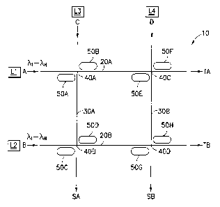
to FIG. 4,
wherein the quantities M and N both equal 2. Specifically, two first
waveguides 20A, 20B are
intersected by two second waveguides 30A, 30B, with four nodes 40A-D being
defined. In
addition, a respective two of the switching elements SOA-H are disposed in
proximity to each of
the nodes 40A-D. In the same manner as described above, portions of light
signals may be
added and dropped between the first waveguides 20A, 20B and the second
waveguides 30A,
30B. Table 1 sets forth possible workings of the optical cross-connect of FIG.
4, wherein the
switching elements SOA-H may or may not be tuned. (For purposes of Table l,
all switching
elements SOA-H are tuned to the same wavelength, when tuned.)
Table 1.
SWITCHING OUTPUT OF OUTPUT OUTPUT OF OUTPUT OF
ELEMENTS INPUT SIGNALOF INPUT SIGNALINPUT SIGNAL
SOA-H A INPUT SIGNALC D
(TUNED=Y; B
NOT
TUNED=N)
A
B
C
D
E
F
G
H
Y Y Y Y N N N N TB SA TA SB
N N N N Y Y Y Y TB SB SA TA
N N Y Y N N Y Y TA SA SB TB
As is readily apparent, any quantities M and N of the first and second
waveguides 20, 30,
respectively, can be used in similar fashion with signals and portions of
signals being transferred
from waveguide to waveguide to reach a desired destination. Moreover, with the
tuning of
switching elements, different portions of the light signals may be
controllably transferred.
CA 02374685 2001-11-19
WO 00/72063 _ g _ PCT/US00/13728
With continued reference to FIG. 4, and by way of non-limiting example, the
operation
of the inventive optical switch 10 will now be discussed in detail. Four
optical sources L1-L4
generate input signals, designated as A, B, C, and D, which are caused to
propagate respectively
through the waveguides 20A, 20B, 30A, and 308. The input signals A-D may each
be an optical
signal comprised of a plurality of wavelengths, or alternatively, comprised of
a single
wavelength, as a routine matter of design choice. For example, optical source
L1 may provide
input signal A to waveguide 20A comprised of wavelengths 7~, - 7~N. If
resonator SOA is tuned to
wavelength 7~i, that wavelength is coupled from the optical signal propagating
through
waveguide 20A by resonator SOA and into waveguide 30A, i.e., that wavelength
is dropped from
the optical signal in waveguide 20A and output from the optical switch 10 via
waveguide 30A.
The remaining wavelengths in the input signal A continue propagating through
waveguide 20A
(i.e., the non-coupled wavelengths), pass-through node 40A, and exit the
optical switch 10 via
waveguide 20A. Optical source L3 may also provide a mufti- or single-
wavelength optical
signal as input signal C to waveguide 30A, which may be selectively coupled
between and
among waveguides 20A, 20B, and 30B, and which may also pass-through waveguide
30A,
depending upon the selective tuning of the various resonators SOA-H provided
as part of the
optical switch 10. For example, if the input signal C provided by optical
source L3 includes
wavelength ~,,, that wavelength may be coupled from waveguide 30A to waveguide
20A by
resonator SOA, which is tuned to that wavelength. Various other coupling
configurations may be
provided in accordance with the present invention, depending upon the
composition of the
optical signals propagating through the various waveguides 20A, 20B, 30A, 30B,
and further
depending upon the selective tuning of the resonators SOA-H.
As a further embodiment, reference is made to FIG. 5, wherein four of the
switching
elements SOI-L are located in proximity to the node 40. Advantageously, with
four of the
switching elements SOI-L light signals may be passed through either of the
waveguides 20, 30
CA 02374685 2001-11-19
WO 00/72063 - g _ PCT/US00/13728
and switched in either direction. Stated differently, by having switching
elements 50 between
each pair of adjoining portions 201-301, 301-202, 202-302, 302-201 of the
waveguides 20, 30,
signals, or portions thereof, may be switched between the adjoining waveguides
20, 30. In
contrast, with reference to FIG. 3 by example, light signals may not be
switched about regions A
and B. Thus, a signal propagating rightwardly through the waveguide 20 could
not be switched
upwardly to propagate through the waveguide 30, and vice versa.
In addition to using oval resonators as the switching elements 50, elliptical
resonators
500 can be used, such as that shown in FIG. 6, and circular resonators 501 can
be used, such as
that shown in FIG. 7. With an elliptical resonator 500, it is preferred that
the major axis (MA) of
the resonator be generally parallel to the first waveguide 20, and the minor
axis (NA) be
generally parallel to the second waveguide 30. In addition, the switching
elements 50 may be
MEMS (micro-electromechanical system) switches with mirrors.
Furthermore, the switching element SO may be a directional coupler where
frequency
selectivity is not a concern, such as that shown in FIG. 8 and designated with
reference numeral
502. Directional couplers are known in the prior art. Copending U.S. Patent
Application
to the same inventors and assignee herein, discloses a directional coupler
utilizable with the subject invention, and said disclosure is incorporated by
reference herein.
The directional coupler 502 includes straight portions 503 and a curved
portion 504
which faces the node 40. The straight portions 503 are generally parallel to
portions of the first
waveguides 20 and the second waveguide 30, respectively. In use, the
directional coupler 502
causes coupling of an entire light signal propagating through the first
waveguide 20 to the
second waveguide 30 in a deactivated state (i.e., no electrical voltage being
applied). With an
electric voltage being applied, the directional coupler 502 is activated, and
the entire light signal
passing through the first waveguide 20 will by-pass the directional coupler
without there being
any coupling of signal to the second waveguide 30. The directional coupler 502
is formed and
CA 02374685 2001-11-19
WO 00/72063 _ 1p _ PCT/US00/13728
positioned to achieve the necessary coupling in a deactivated state (i.e.,
proper coupling lengths;
gap width between directional coupler and waveguides, etc., are provided).
In another aspect of the invention, referring to FIGS. 9A and 9B, portions of
the
waveguides 20, 30 at, and in proximity to, the nodes 40 are enlarged to
increase the area of the
nodes 40. Thus, the waveguides 20, 30 are each formed with a width w at, and
in proximity to,
the nodes 40 which is greater than the width h of the remaining portions of
the waveguides 20,
30. The waveguides 20, 30 need not have the same widths w or the same widths
h.
Additionally, the enlarged portions of the waveguides 20, 30 may be connected
with remaining
portions of the waveguides 20, 30 either with straight tapered portions 90
(FIG. 9A) or arcuate
portions 100 (FIG. 9B). With an enlarged area, less diffraction occurs at the
nodes 40 and, thus,
signal cross-talk is reduced of signals passing through the nodes 40.
Additionally, signal loss is
reduced.
The first and second waveguides 20, 30 can be arranged in a perpendicular
matrix
arrangement, as shown in FIG. 4. Alternatively, with reference to FIG. 10, the
first and second
waveguides 20, 30 can be arranged with portions thereof being generally
parallel. As shown in
FIG. 10, a straight portion 110 of the first waveguide 20 is generally
parallel to a straight portion
120 of the second waveguide 30. In addition, returning to the preferred
embodiment, the straight
portions 52 of the oval resonator 50 are also arranged generally parallel to
the straight portions
110, 120. With this arrangement, the oval resonator 50 has straight portions
52 coupling with
the straight portions 110, 120, thereby increasing the efficacy of signal
transference.
Additionally, the oval resonator 50 can be used to transfer signals between
both the first
waveguide 20 and the second waveguide 30.
Thus, while there have been shown and described and pointed out fundamental
novel
features of the invention as applied to preferred embodiments thereof, it will
be understood that
various omissions and substitutions and changes in the form and details of the
disclosed
CA 02374685 2001-11-19
WO 00/72063 _ 11 _ PCT/US00/13728
invention may be made by those skilled in the art v~ithout departing from the
spirit of the
invention. It is the intention, therefore, to be limited only as indicated by
the scope of the claims
appended hereto.