Note: Descriptions are shown in the official language in which they were submitted.
CA 02375345 2001-11-26
WO 01/88623 PCT/USO1/15510
METHOD FOR USING HARD MAGNETIC CARRIERS IN AN ELECTROGRAPHIC
PROCESS
Cross Reference to Related Applications
This Application claims benefit under 35 USC ~119(e) of prior co-pending U.S.
Provisional Patent Application, Serial No. 60/204,941, filed May 17, 2000, the
disclosure of
which is incorporated herein by reference in its entirety. Attention is also
directed to the
following related U.S. patent applications: U.S. Serial No. 09/572,988
entitled "MAGNETIC
to CARRIER PARTICLES"; and U.S. Serial No. 09/572,989 entitled "MAGNETIC
CARRIER
PARTICLES", both filed on May 17, 2000, the disclosures of which are also
incorporated
herein by reference in their entirety.
Background of the Invention
This invention relates to electrography and more particularly it relates to
magnetic
carrier particles and developers used for the dry development of electrostatic
charge images.
In electrography, an electrostatic charge image is formed on a dielectric
surface,
typically the surface of the photoconductive recording element. Development of
this image is
typically achieved by contacting it with a two-component developer comprising
a mixture of
2o pigmented resinous particles, known as toner, and magnetically attractable
particles, known
as carrier. The carrier particles serve as sites against which the non-
magnetic toner particles
can impinge and thereby acquire a triboelectric charge opposite to that of the
electrostatic
image. During contact between the electrostatic image and the developer
mixture, the toner
particles are stripped from the carrier particles to which they had formerly
adhered (via
2s triboelectric forces) by the relatively strong electrostatic forces
associated with the charge
image. In this manner, the toner particles are deposited on the electrostatic
image to render it
visible.
It is generally known to apply developer compositions of the above type to
electrostatic images by means of a magnetic applicator, also known as a
magnetic brush,
3o which comprises a cylindrical sleeve of non-magnetic material having a
magnetic core
positioned therein. The core usually comprises a plurality of parallel
magnetic strips arranged
around the core surface to present alternating north and south oriented
magnetic fields.
These fields project radially, through the sleeve, and serve to attract the
developer
composition to the sleeve outer surtace to form what is commonly referred to
in the art as a
1
CA 02375345 2001-11-26
WO 01/88623 PCT/USO1/15510
"brush" or "nap". Either or both the cylindrical sleeve and the magnetic core
are rotated with
respect to each other to cause the developer to advance from a supply sump to
a position in
which it contacts the electrostatic image to be developed. After development,
the toner
depleted carrier particles are returned to the sump for toner replenishment.
Conventionally, carrier particles made of soft magnetic materials have been
employed
to carry and deliver the toner particles to the electrostatic image. U.S. Pat.
Nos. 4,546,060,
4,473,029 and 5,376,492, the teachings of which are incorporated herein by
reference in their
entirety, teach use of hard magnetic materials as carrier particles and also
apparatus for
development of electrostatic images utilizing such hard magnetic carrier
particles. These
to patents require that the carrier particles comprise a hard magnetic
material exhibiting a
coercivity of at least 300 Oersteds when magnetically saturated and an induced
magnetic
moment of at least 20 EMU/gm when in an applied magnetic field of 1000
Oersteds. The
terms "hard" and "soft" when referring to magnetic materials have the
generally accepted
meaning as indicated on page 18 of Introduction To Magnetic Materials by B. D.
Cullity
published by Addison-Wesley Publishing Company, 1972. These hard magnetic
carrier
materials represent a great advance over the use of soft magnetic carrier
materials in that the
speed of development is remarkably increased with good image development.
Speeds as
high as four times the maximum speed utilized in the use of soft magnetic
carrier particles
have been demonstrated.
2o In the methods taught by the foregoing patents, the developer is moved in
the same
direction as the electrostatic image to be developed by high-speed rotation of
the multi-pole
magnetic core within the sleeve, with the developer being disposed on the
outer surface of
the sleeve. Rapid pole transitions on the sleeve are mechanically resisted by
the carrier
because of its high coercivity. The nap, also called "strings" or "chains", of
carrier (with toner
particles disposed on the surface of the carrier particles), rapidly "flips"
on the sleeve in order
to align with the magnetic field reversals imposed by the rotating magnetic
core, and as a
result, moves with the toner on the sleeve through the development zone in
contact with or
close relation to the electrostatic image on a photoconductor. This
interaction of the
developer with the charge image is referred to as "contact" or "contacting"
herein for purposes
of convenience. See also, U.S. Patent 4,531,832, the teachings of which are
also
incorporated herein in their entirety, for further discussion concerning such
a process.
The rapid pole transitions, for example as many as 467 per second at the
sleeve
surface when the magnetic core is rotated at a speed of 2000 revolutions per
minute (rpm),
create a highly energetic and vigorous movement of developer as it moves
through the
2
CA 02375345 2001-11-26
WO 01/88623 PCT/USO1/15510
development zone. This vigorous action constantly recirculates the toner to
the sleeve
surface and then back to the outside of the nap to provide toner for
development. This
flipping action thus results in a continuous feed of fresh toner particles to
the image. As
described in the above-described patents, this method provides high density,
high quality
images at relatively high development speeds.
The above-mentioned U.S. patents, while generic to all hard magnetic materials
having the properties set forth therein, prefer the hard magnetic ferrites
which are compounds
of barium and/or strontium, such as, BaFe~~0~9, SrFe~20~9 and the magnetic
ferrites having
the formula M0.6Fe203, where M is barium, strontium or lead as disclosed in
U.S. Pat. No.
l0 3,716,630. While these hard ferrite carrier materials represent a
substantial increase in the
speed with which development can be conducted in an electrostatographic
apparatus, many
users of such equipment seek even faster development speeds and so further
improvements
to the carrier and development process are of interest.
U.S. Patent 4,764,445 discloses hard magnetic ferrite carrier particles for
electrographic developing applications which contain from about 1 to about 5
percent by
weight of lanthanum. As mentioned in this patent, the speed of development in
an
electrographic process using conventional hard magnetic ferrite materials,
while higher than
methods using other techniques, such as with soft magnetic carriers, is
limited by the
resistivity of such ferrite materials. The patent discloses that addition of
lanthanum to the
hard magnetic ferrite crystal structure in the disclosed amounts results in a
more conductive
magnetic ferrite particle, yielding greater development efficiency and/or
speed of
development.
Others have also proposed methods for making conductive carrier particles. For
example, U.S. Patent 4,855,206 discloses adding neodymium, praseodymium,
samarium,
europium, or mixtures thereof, or a mixture of one or more of such elements
and lanthanum,
to a hard magnetic ferrite material to increase conductivity. U.S. Patent
5,795,692 discloses
a conductive carrier composition having a magnetic oxide core which is said to
be coated with
a layer of zinc metal that is the reaction product of zinc vapor and the
magnetic oxide.
Other carriers proposed for use in an electrographic process include multi-
phase
3o ferrite composites as taught in U.S. Patents 4,855,205; 5,061,586;
5,104,761; 5,106,714;
5,190,841; and 5,190,842.
U.S. Patent 5,268,249 discloses magnetic carrier particles with a single-
phase, W-
type hexagonal crystal structure of the formula MFe~6Me~02, where M is
strontium or barium
3
CA 02375345 2001-11-26
WO 01/88623 PCT/USO1/15510
and Me is a divalent transition metal selected from nickel, cobalt, copper,
zinc, manganese,
magnesium, or iron.
U.S. Patent 5,532,096 discloses a carrier which has been coated on the surface
thereof with a layer obtained by curing a partially hydrolyzed sol obtained
from at least one
~ alkoxide selected from the group consisting of silicon alkoxides, titanium
alkoxides, aluminum
alkoxides, and zirconium alkoxides. The disclosed carriers coated with such
layer are said to
be more durable in comparison to carriers coated with conventional resin
coatings, such as
those prepared using silicone, acrylic and styrene-acrylic resins.
While some of the above-described patent art may describe carriers with
increased
to conductivity relative to traditional hard magnetic ferrite materials
previously employed in
development of electrostatic images, the conductivity of the carriers is
believed to be so great
that imaging problems are typically created due to the carrier being deposited
in the image.
Although not clear, it is believed that certain levels of conductivity in the
carrier can facilitate a
flow of charge between the carrier on the nap and the shell, thereby inducing
a charge
reversal on the carrier and allowing the carrier particles to
electrostatically deposit on the
image, referred to hereinafter as "image carrier pick-up" or "I-CPU". The
presence of I-CPU
can impact color rendition and image quality.
As can be seen, it would be desirable to develop new carriers and/or new
methods for
use of carriers that can be used in an electrographic process for the
development of latent
electrostatic images. It would also be desirable to develop carriers that can
exhibit a greater
level of conductivity relative to traditional hard magnetic materials
previously employed in
such processes, which can provide electrographic methods having higher levels
of
development efficiency with reduced levels of I-CPU.
Summary of the Invention
The foregoing objects and advantages are realized by the present invention,
which, in
one aspect, concerns a method for development of an electrostatic image
comprising
contacting the image with a development system including at least one magnetic
brush
comprising:
3o (a) a rotating magnetic core of a pre-selected magnetic field strength,
(b) an outer nonmagnetic shell disposed about the rotating magnetic core, and
(c) an electrographic developer composition comprising (i) charged toner
particles,
and (ii) oppositely charged hard magnetic carrier particles with a resistivity
of
from about 1x10'° ohm-cm to about 1x10⁵ ohm-cm and a (Q/m) career of
greater
4
CA 02375345 2001-11-26
WO 01/88623 PCT/USO1/15510
than about 1 pC/g, the developer composition being disposed on the shell and
in contact with the image,
the method resulting in a carrier deposition density on the image of less than
about 0.01 g/in2.
In another aspect, the invention concerns a method for development of an
electrostatic image comprising contacting the image with at least one magnetic
brush
comprising (a) a rotating magnetic core of a pre-selected magnetic field
strength, (b) an outer
nonmagnetic shell disposed about the rotating core, and (c) an electrographic
developer
composition disposed on the shell and in contact with the image. The developer
composition
comprises charged toner particles and opposite(y charged carrier particles,
the carrier
particles comprising a hard magnetic material having a crystal structure
substituted with at
least one multi-valent metal of the formula M"+, wherein n is an integer of at
least 4.
In a preferred embodiment, the carrier particles comprise a hard magnetic
ferrite
material having a single-phase hexagonal crystal structure and represented by
the formula:
PFela_xMxO~s
wherein:
P is selected from strontium, barium, or Lead;
2o M is at least one metal selected from antimony, arsenic, germanium,
hafnium,
molybdenum, niobium, silicon, tantalum, tellurium, tin, titanium, tungsten,
vanadium, zirconium, and mixtures thereof; and
x is less than about 0.6.
in another aspect, the invention concerns a method for development of an
electrostatic image comprising contacting the image with at least one magnetic
brush
comprising (a} a rotating magnetic core of a pre-selected magnetic field
strength, (b) an outer
nonmagnetic shell disposed about the rotating core, and (c) an electrographic
developer
composition disposed on the shell and in contact with the image, the developer
composition
comprising charged toner particles and oppositely charged carrier particles.
The carrier
3o particles comprise (1) a core of a hard magnetic material having an outer
surface and (2) a
metal oxide composition disposed on the outer surface of the core represented
by the formula
MOn,2 wherein M is at least one mufti-valent metal represented by M"~, with n
being an integer
of at least 4. The outer surface further defines a transition zone which
extends from the outer
surface and into the core of the hard magnetic material where the hard
magnetic material has
s
CA 02375345 2001-11-26
WO 01/88623 PCT/USO1/15510
a crystal structure within the transition zone substituted with ions of the at
least one multi-
valent metal ion of formula M"+ as previously described.
In another aspect, the invention relates to a method for development of an
electrostatic image comprising contacting the image with at least one magnetic
brush
comprising (a) a rotating magnetic core of a pre-selected magnetic field
strength, (b) an outer
nonmagnetic shell disposed about the rotating core, and (c) an electrographic
developer
composition disposed on the shell and in contact with the image, the developer
composition
comprising charged toner particles and oppositely charged carrier particles.
The carrier
particles comprise a hard magnetic ferrite material having a single-phase
hexagonal crystal
1o structure represented by the formula:
P~_yLayFe~20vs
wherein:
P is selected from strontium, barium, or lead; and
y is less than 0.1.
Also disclosed are carrier particles for use in the development of
electrostatic latent
images, which carriers comprise the hard magnetic ferrite material substituted
with lanthanum
as described in the preceding paragraph.
Brief Description of the Drawings
Fig. 1 is a graph of toner charge-to-mass (Q/m) versus toner concentration for
a
developer used in a method according to the present invention, the figure
showing operating
windows for three different toner particle sizes and illustrating an operating
region for each
which can yield desirable electrographic system performance.
Fig. 2 is a graph of both relative development efficiency (as defined
hereinafter) and
I-CPU data obtained in connection with Examples 5-7 and Comparative Example B
discussed
hereinafter.
Fig. 3 is a graph of both relative development efficiency (as defined
hereinafter) and
3o t-CPU data obtained in connection with Examples 8-10 and Comparative
Example C
discussed hereinafter.
Fig. 4 is a graph of resistivity (in ohm-cm) versus firing temperature for
carriers
prepared and evaluated in connection with Examples 11-13 and Comparative
Example D
discussed hereinafter.
6
CA 02375345 2001-11-26
WO 01/88623 PCT/USO1/15510
Fig. 5 is a graph of I-CPU (grams deposited) versus (Q/m) carrier data
relating to
Examples 43-46 and is discussed at the end of Example 46 hereinafter.
Fig. 6 is a graph of Mean Relative DE data versus toner particle size relating
to
Examples 43-52 and is discussed at the end of Example 52 hereinafter.
Fig. 7 is a graph of Mean (Q/m) toner data versus toner particle size relating
to
Examples 43-52 and is discussed at the end of Example 52 hereinafter.
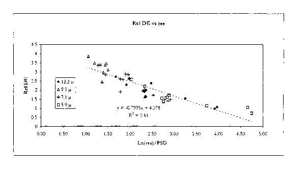
Fig. 8 is a graph of Relative DE data versus Loge of (carrier
resistivity/toner particle
size) relating to Examples 43-52 and is discussed at the end of Example 52
hereinafter.
Fig. 9 is a graph of I-CPU (weight in grams) versus a function representing
acquired
to carrier charge (in terms of pC/g) relating to Examples 43-52 and
Comparative Example E,
and is discussed at the end of Example 52 hereinafter.
Detailed Description of the Invention
As previously pointed out in connection with U.S. Pat. Nos. 4,546,060 and
4,473,029,
the use of "hard" magnetic materials as carrier particles increases the speed
of development
dramatically when compared with carrier particles made of "soft" magnetic
particles. The
preferred ferrite materials disclosed in these patents include barium,
strontium and lead
ferrites having the formula M0.6Fe~03 wherein M is barium, strontium or lead.
A preferred
ferrite is strontium ferrite. These materials have a single-phase, hexagonal
crystal structure.
2o While the speed with which development can be carried out is much higher
than prior
techniques, they are limited by the resistivity of the above described ferrite
materials which
have the necessary magnetic properties for carrying out the development
method. It is
generally known that the resistivity of the carrier particles bears a direct
result on the speed of
development that can be employed.
While development speed is generally referred to in the art, a more meaningful
term is
to speak of "development efficiency". In a magnetic brush development system,
development
efficiency in percent is defined as the potential difference between the
photoreceptor in
developed image areas before and after development divided by the potential
difference
between the photoreceptor and the brush prior to development times 100. For
example, in a
3o charged area development configuration, if the photoreceptor film voltage
is -250 volts and
the magnetic brush is -50 volts, the potential difference is -200 volts prior
to development. If,
during development, the film voltage is reduced by 100 volts to -150 volts in
image areas by
the deposition of positively charged toner particles, the development
efficiency is (-100 volts
divided by -200 volts) times 100, which gives an efficiency of development of
50 percent. It
CA 02375345 2001-11-26
WO 01/88623 PCT/USO1/15510
can be readily seen that as the efficiency of the developer material increases
the various
parameters employed in the electrostatographic method can be altered in
accordance
therewith. For example, as the efficiency increases the voltage differential
prior to
development can be reduced in order to deposit the same amount of toner in
image areas as
was previously done at the lower efficiency. The same is true with regard to
the exposure
energy level employed to impart the latent electrostatic image on the
photoreceptor film. The
speed of the development step of the procedure can be increased as the
efficiency increases
since more toner can be deposited under the same conditions in a shorter
period of time.
Thus, higher development efficiency permits adjustment of the various
parameters employed
to in the electrostatic process to result in savings in both energy and time.
As previously mentioned the efficiency of development when employing hard
magnetic carriers is limited by the resistivity of the materials themselves.
For example,
because these materials have a resistivity of approximately 1x10" ohm-cm,
therefore, the
efficiency typically obtained is approximately 50 percent. However, in order
to obtain high
quality copies of the original image, it is necessary to maintain high
magnetic properties; i.e. a
coercivity of at least about 300 Oersteds when magnetically saturated and an
induced
magnetic moment of at least about 20 EMU/gm when in an applied field of 1000
Oersteds
while at the same time increasing the conductivity of the particles.
The electrophotographic printing industry is presently interested in
developing
2o equipment with higher speed (pages per minute - ppm) and higher image
quality. These two
performance goals require materials, i.e., developer compositions, With
characteristics that
are in contraposition to each other. Higher image quality is associated with
smaller toner
particle size. Smaller toner size generally connotes reduced development
efficiency (DE),
and as such, limits machine speed. While adjustment of hardware operating
conditions such
as core speed, shell speed, gap setting and toning bias provide considerable
latitude for high
speed/high quality copying/printing, the material characteristics of the
carrier component of
the developer may also be manipulated.
The realization of increased development efficiency through the application of
conductive carriers is limited by the image carrier pickup (I-CPU). This
behavior follows from
3o an induced reversal charge on carrier particles in the brush under the
influence of the bias
and contact with the shell. The carrier particles of reversed polarity are
electrostatically
attracted to the charge image on the photoconductor; in effect, these
particles act as toner
and deposit in the image accordingly. Conductive carriers are believed to be
more
susceptible to this charge reversal, because of the increased charge mobility
associated with
s
CA 02375345 2001-11-26
WO 01/88623 PCT/USO1/15510
higher conductivity. The presence of carrier in the image area is not
particularly detrimental
in black and white text documents; however, it confounds flat black and white
images and
severely impacts rendition, gamut and density in color documents.
While not wishing to be bound by theory, it is believed that I-CPU depends on
carrier
charge. In a developer composition comprising carrier particles and toner
particles, the
carrier charge is opposite in polarity to the toner charge. For conventional,
non-conductive
carrier, when toner is developed into the image during development, the
carrier can be
developed into background areas of the image, usually at a highest
concentration in areas
immediately adjacent to toned image areas where fringe electric fields are
strongest. For
to carriers with higher levels of conductivity, due to the charge mobility
mentioned above,
electric charge can be conducted into the carrier particles from the toning
shell when the
developer composition is in the electric field of a "toning nip", i.e., the
area between the
photoconductive surface (whereon the latent electrostatic image being
developed resides)
and the surface of the shell sleeve for the toning station (whereon the
developer composition
resides). For discharged area development (DAD), the bias voltage of the
toning station is
the same polarity as the toner and the toning bias can therefore charge a
conductive carrier
to the same polarity as the toner. If the carrier acquires sufficient charge
by conduction of
such charge from the shell within the toning nip, the carrier can actually
develop into image
areas on the photoconductor.
2o A negative-charging toner is considered in the following discussion.
Assuming charge
neutrality for the toner and carrier particles, when the externally applied
electric field (E) is
zero, the carrier charge and the toner charge in the developer composition may
be related to
toner concentration (TC) according to the following Equation (1):
QTIMT X TC+Qc/MC x (1-TC) = 0 (1)
wherein QT and Qc represent the charge of the toner and carrier respectively;
MT and M~
represent the mass of the toner or carrier respectively; x signifies
multiplication (not a
variable); and TC is the fractional toner concentration based on total weight
of the
3o composition, or the toner concentration in weight percent, divided by 100.
Therefore, the
initial carrier charge to mass ratio (in pC/g) can be stated by the following
Equation (2):
Qcs~c - -QT/MT x TC/(1-TC) (2)
9
CA 02375345 2001-11-26
WO 01/88623 PCT/USO1/15510
As the developer composition moves into the electric field of the toning nip
area, it is believed
that the carrier loses its initial positive charge and becomes more negative
in charge by the
conductive charge mechanism as previously described. If there is sufficient
residence time
within the toning nip area, the carrier can acquire a large enough negative
charge that it will
develop into the image areas with the toner.
Although not bound by theory, it is reasonable to assume that the initial
carrier charge
is approximated by Equation (2) and the carrier charge in the toning nip area
follows an
exponential time dependence, as illustrated for example by Equation (3) below:
l0
QCt/MC = Qc~/Mcx e-kc ,+ QCf/MC~ ~1-a ~~ (3)
wherein QCt/MC IS the carrier charge to mass as a function of time; Qc~/Mc is
the initial
carrier charge to mass as described above; the rate constant k is 1/ps, in
units of sec'; x
signifies multiplication (not a variable); t is the residence time in the
toning nip in seconds;
and the maximum final carrier charge is given by Qcf/Mc.
In Equation (3), quantitatively p is the resistivity of the developer
composition and E is
the dielectric constant of the developer composition. The developer
resistivity p can be
measured as described in Examples 43-52 hereinafter. The dielectric constant s
is affected
2o by the volume in the developer composition that is occupied by the toner.
Increasing the
toner particle size will displace carrier particles and correspondingly result
in a proportionate
decrease the dielectric constant of the developer composition. Due to this
effect, E ~ 1/ pTS,
where DT is the average particle size (diameter) of the toner particles.
The maximum carrier charge to mass ratio Qcf/Mc depends on the voltage
difference
between the electrostatic image on the photoconductive surface and the toning
station shell
sleeve. For a 400 volt potential difference with "bare carrier" (no toner),
Qcf/Mc can be
reasonably assumed to be about -2 ~.C/g. If toner is present, the potential
difference between
the shell sleeve and photoconductive surface at the trailing edge (exit) of
the toning nip area
is decreased by the charge of toner particles which develop into the image.
The fractional
3o development efficiency - DE - can be approximated as the fraction of the
initial toning
potential difference removed by development of the toner, and equals the
development
efficiency in percent divided by 100. For a 400 V toning potential, Qcf/Mc~ -2
x (1-DE) in
to
CA 02375345 2001-11-26
WO 01/88623 PCT/USO1/15510
terms of pC/g. This equation states that, if the development efficiency is
large, there is less
potential to drive charge into the carrier, and the maximum carrier charge to
mass ratio is
reduced proportionally. Data obtained in connection with Examples 43-52 and
Comparative
Example E hereinafter is used with the above-described model and confirms that
I-CPU
depends upon the charge that the carrier acquires in the toning nip area.
The present invention further relates to material and hardware parameters that
provide operating spaces for higher development efficiency without increased I-
CPU.
improvements in development efficiency can be obtained without a concurrent
increase in I-
CPU if certain material and hardware operating conditions are met.
to A general relationship for such operating spaces in terms of toner charge-
to-mass
(Q/m) and toner concentration (TC) for different toner particle sizes is shown
in Figure 1. Fig.
1, which is provided for discussion purposes, illustrates that smaller
particle size toners tend
to operate preferably at lower toner concentrations and exhibit higher toner
charge-to-mass.
These relationships hold for either polarity toner.
In tabular form, along with the associated change in development efficiency
and the
implied carrier conductivity to regain development efficiency, the
relationships can be
described as follows:
Required
Toner Toner Development Carrier
size Q/m Efficiency Conductivity
In the table above, the arrows represent an increase or decrease in the
associated
parameter. To counteract the expected drop in development efficiency by using
smaller toner
sizes, it is desirable to use a carrier with greater conductivity as indicated
by the upward
pointing arrow under the heading "Required Carrier Conductivity".
The drive to higher quality and higher speed systems necessitates a decrease
in toner
particle size from which a decrease in development efficiency follows. To
regain
development efficiency, the carrier conductivity should be further increased
(in other words,
3o the carrier's resistivity should be decreased) as the toner size decreases.
To be viable, the
enhancement in development rate should occur without noticeable I-CPU.
To address the reduction of I-CPU, the toner size/concentration/charge space
as
illustrated by Fig. 1 is unwieldy and difficult to generalize over all
anticipated operating
ranges. For each toner size, a table could be set up with data sets to
indicate, for example,
11
CA 02375345 2001-11-26
WO 01/88623 PCT/USO1/15510
using each of the three toner sizes shown in Fig. 1, the resistivity range
required to maintain
development efficiency along with the preferred range for limited I-CPU. An
alternate
approach utilized in connection with Examples 43-52 hereinafter, is to
characterize the
development performance of a developer composition by parameters of primary
merit, i.e.,
the carrier charge-to-mass - (Q/m) carrier - (in terms of pC/g) and developer
composition
resistivity (in ohm-cm).
Data generally shows that the developers exhibiting the highest I-CPU have the
lowest calculated (Q/m) carrier as determined by charge neutrality. For
example, as the toner
concentration increases, the toner charge decreases by a small percentage,
however, the net
to (Q/m) carrier can double or triple in value. The higher the net (Q/m)
carrier the more difficult it is
to induce the charge reversal of the carrier leading to I-CPU. As one goes to
a smaller toner
particle size, the increased toner Q/m can reduce I-CPU, but the lower toner
concentration
could also induce I-CPU. As a result, it is desirable that (Q/m) carrier be
maintained at greater
than about 1 pClg, preferably greater than about 2 pC/g, more preferably
greater than about
is 3 ~,C/g, and most preferably greater than about 4.0 pC/g. The (C~/m)
carrier parameter can be
controlled by adjusting the level of toner in the developer composition, as
illustrated for
example in Examples 43-52 hereinafter.
As such, the present invention seeks to at least maintain development
efficiency as
toner size decreases, and therefore conductivity of the carrier should be
increased
2o proportionally, while (Q/m) carrier should be kept high, such as a value
greater than about 1
~C/g as previously described. In addition, to obtain high quality copies with
minimum
amounts of I-CPU, it is preferable to maintain the resistivity of the carrier
to a value of from
about 1x10'° ohm-cm to about 1x10⁵ ohm-cm, more preferably from about
5x10⁹ ohm-cm to
about 1x10⁶ ohm-cm, and even more preferably from about 5x10⁹ ohm-cm to about
1x10'
2s ohm-cm. When the carrier resistivity is selected to be within the foregoing
range, it will
generally result in a developer composition resistivity of desirably from
about 1x10'2 ohm-cm
to about 1x10⁵ ohm-cm, preferably 1x10'° ohm-cm to 1x10' ohm-cm. The
developer
resistivity will generally be very similar to the carrier resistivity, since
the developer
composition is largely carrier.
3o Electrographic processes can operate at a process speed (which is defined
as the
speed at which the dielectric surface bearing the charge image thereon is
passed through the
development zone) of at least about 5 incheslsec, and typically high volume
printers can
operate at a speed of from about 110 pages per minute (PPM) to 180 PPM and up,
which
corresponds to a process speed of from about 15 to about 30 inches/sec, and a
process
12
CA 02375345 2001-11-26
WO 01/88623 PCT/USO1/15510
speed of from about 15 to about 50 inches/sec would be preferred. Carriers
with a resistivity
toward the lower part of the foregoing ranges, i.e., a resistivity of less
than about~1x10' ohm-
cm, i.e., from about 1x10' ohm-cm to about 1x10⁵ ohm-cm, would be particularly
advantageous for use in electrographic processes operating at relatively high
process
speeds. This is due to the fact that a higher process speed results in a
proportional decrease
in the residence time of carrier within the toning nip area, wherein residence
time (in seconds)
is defined as the toning nip width (in inches) divided by the process speed
(in inch/sec). For
example, if a given carrier is exhibiting some I-CPU or I-CPU which is at or
near a level which
is unacceptable, when the carrier is used in a developer composition at a
given process
to speed, the process speed can be increased to reduce the residence time of
carrier in the
toning nip area and obtain a decrease in I-CPU. Alternatively, increasing
process speed by a
factor of ten, such as from 5 inch/sec to 50 inch/sec, would allow one to
utilize a carrier with a
resistivity reduced by a factor of ten, i.e., for example, from 1x10⁶ to 1x10⁵
ohm-cm, and
obtain similar I-CPU performance. Similarly, the geometry of the toning nip
area can be
altered, for example, so as to decrease the width of the toning nip area. This
could be
achieved, for example, by placing the photoconductive surface on a cylindrical
drum, or if the
surface is already on a drum, then by reducing the diameter of such drum. A
reduction in the
toning nip width by a factor of two, would similarly translate to a reduction
in resistivity for the
carrier by a factor of two as well.
2o According to the invention, I-CPU can be limited such that, in terms of
deposition
density for carrier (as described in Examples 43-52 hereinafter), such
deposition density is
desirably less than about 0.01 g/in2, preferably less than about 0.001 g/in2,
and more
preferably less than about 0.0001 g/in2.
In preferred embodiments, the present invention contemplates use of certain
hard
magnetic materials as a carrier in an electrographic process, wherein the
carrier has
increased conductivity relative to conventionally used hard magnetic
materials. In one
embodiment, the carrier is a hard magnetic material substituted with multi-
valent metals to
increase the conductivity of the carrier. In another embodiment, a conductive
metal oxide
composition is placed on a core of a hard magnetic material. Both are
discussed hereinafter.
3o While there is discussion of these embodiments in some detail hereinafter,
including the
examples, it is not intended to limit the invention to these particular
embodiments. It should
be understood that other hard magnetic materials may be used in practicing the
invention,
provided they have the requisite conductivity and (Q/m) carrier parameters,
and that they are
otherwise used with the appropriate operating parameters for the methods
described herein.
13
CA 02375345 2001-11-26
WO 01/88623 PCT/USO1/15510
Conductive Carriers Substituted with Multi-Valent Metals
The present invention, in one embodiment, contemplates use of carriers
substituted
with an effective amount of at least one multi-valent metal ion into the
crystalline lattice of a
hard magnetic material, preferably a hard magnetic ferrite having a hexagonal
crystal
structure, the metal ion corresponding to the formula M"+, where n is an
integer of at least 4,
i.e, 4, 5, or 6, so as to reduce the resistivity of the material white stiff
maintaining desirable
magnetic properties. Thus, the resistivity of hard hexagonal ferrite carrier
materials can be
reduced from approximately 1x10" to approximately 1x10⁵ ohm-cm, and preferably
the
1o resistivity and (Q/m) carrier are within the ranges specified hereinabove
for inhibiting I-CPU,
without affecting the high magnetic properties of the ferrite material.
While not wishing to be bound by theory, it is believed, from size and charge
considerations of the cations to be substituted, that the mechanism by which
the resistivity of
the ferrite materials are decreased is due to substitution of the above-
described multi-valent
metal ion into the iron lattices of the hexagonal ferrite crystal structure,
rather than by
replacement of Srz+ Ba2+, or Pb2+ in the sub-lattice or interstitially in the
hexagonal ferrite
lattice. In doing so, the M"+ multi-valent metal ion substituents force charge
compensation in
the ferric (Fe3+) lattice; i.e., ferrous (Fey+) cations form. The Fey+/Fe3+
charge couple thereby
created provides a semi-conductive electronic pathway, resulting in ferrite
compositions of
~ higher conductivity.
In a preferred embodiment, a hard magnetic ferrite material doped with the M"+
multi-
valent metal ion can be represented by the formula:
PFe,2_XMXO~s
wherein:
P is selected from strontium, barium, or lead;
M is selected from at least one of antimony, arsenic, germanium, hafnium,
3o molybdenum, niobium, silicon, tantalum, tellurium, tin, titanium, tungsten,
vanadium, zirconium, or mixtures thereof; and
x is less than about 0.6.
14
CA 02375345 2001-11-26
WO 01/88623 PCT/USO1/15510
In especially preferred embodiments, P is selected from either strontium or
barium, and more
preferably strontium due to cost, magnetic properties, and environmental
concerns. M is
preferably selected from silicon, zirconium, tin, or titanium due largely to
cost and availability
concerns. The amount of the mufti-valent metal ion employed is preferably
sufficient to yield
a value for x of less than about 0.3, and more preferably less than about 0.2
due to I-CPU
concerns. If the mufti-valent metal ion is employed in an amount greater than
0.6, the
conductivity does not significantly increase relative to ferrites containing a
lesser amount of
the mufti-valent metal ion. A further advantage associated with the hard
magnetic ferrites of
the present invention is that by conducting a relatively light doping of the
mufti-valent metal
l0 ion into the ferrite material, one can see significant improvement in
development efficiency, as
is exemplified by the examples hereinbelow, as well as in copending U.S.
Patent Application
Serial No. 09/572,988, incorporated herein by reference in its entirety. Also,
with respect to
preparation of such hard magnetic materials, it is believed that substitution
of such metal ions
into the iron lattice offers processing advantages relative to a substitution
into the Sr~+ Baa+, or
Pb2+ sub-lattice.
With respect to the amount of the M"+ mufti-valent metal ion substituted into
the hard
magnetic material, the amount substituted should be sufficient to increase the
conductivity at
least about one order of magnitude, i.e., a reduction in resistivity of at
least about 1x10' ohm-
cm. Preferably, in terms of the x value as mentioned above, the amount of
metal substituted
2o should be sufficient to give an x value of from about 0.01 to about 0.6,
and preferably an
amount sufficient to yield an x value of from about 0.02 to less than about
0.3, and more
preferably an amount sufficient to yield an x value of from about 0.03 to less
than about 0.2 is
employed. It is preferred that the amount of the M"+ mufti-valent metal ion
substituted into the
crystalline lattice be limited such that the resulting structure comprises
substantially a single-
phase hexagonal crystalline structure. While the amount of M"+ mufti-valent
metal ion
employed can vary somewhat depending upon the M"+ mufti-valent metal ion and
sintering
conditions utilized in the preparation of the ferrite particles, the amount of
the M"+ mufti-valent
metal ion can generally be added in an amount of up to about 10 percent by
weight of the
ferrite material and still maintain sufficiently high magnetic properties to
tightly adhere the
3o developer nap to the sleeve of the developer station. As the quantity of
the M"+ mufti-valent
metal ion added exceeds the foregoing range, additional phases in the
PO/MO"~2/Fe203
phase diagram can form. The presence of a minor amount, i.e., preferably less
than 50 wt
based on total weight of carrier, of such additional phases does not adversely
impact the
beneficial properties of a substituted hexagonal crystal structure as
previously described.
CA 02375345 2001-11-26
WO 01/88623 PCT/USO1/15510
The preparation of hard magnetic materials generally, and hard, hexagonal
crystal
structure ferrites (Ba, Sr or Pb) in particular, are well documented in the
literature. Any
suitable method of making the hard magnetic particles may be employed, such as
the
methods disclosed in U.S. Pat. Nos. 3,716,630, 4,623,603 and 4,042,518, the
teachings of
which are incorporated herein by reference in their entirety; European Patent
Application No.
0 086 445; "Spray Drying" by K. Masters published by Leonard Hill Books
London, pages
502-509 and "Ferromagnetic Materials", Volume 3 edited by E. P. Wohlfarth and
published by
North-Holland Publishing Company, Amsterdam, New York, Oxford, pages 315 et
seq, the
teachings of which are also incorporated herein by reference.
l0 Hard magnetic materials containing at least one multi-valent metal ion
substituted into
the crystalline lattice as described hereinabove can be prepared in a similar
manner as
described in the preceding paragraph by adding a source of the multi-valent
metal ion to the
formulation so that the metal ion is doped into the crystalline structure. For
example, if the
hard magnetic material to be prepared is a hard magnetic strontium ferrite
containing from
about 1 to about 5 percent by weight of the multi-valent metal in its oxide or
an oxide
precursor form, then from about 8 to 12 parts SrC03, about 1 to 5 parts of a
source of the
metal ion and 85 to 90 parts of Fe203 are mixed with a dispersant polymer, gum
arabic, and
water as a solvent to form a slurry. The solvent is removed by spray drying
the slurry and the
resultant green beads are fired at from about 1100°C to about
1300°C in an oxidizing
2o environment to form the desired hard magnetic material described above. The
hard magnetic
material is then deagglomerated to yield the component carrier bead particles
with a particle
size generally required of carrier particles, that is, less than about 100 ~m
and preferably from
about 3 to 65 ~.m, and the resulting carrier particles are then permanently
magnetized by
subjecting them to an applied magnetic field of sufficient strength to induce
a permanent
magnetic hysteresis behavior.
In addition to substitution of the foregoing multi-valent metal ions into the
hard
magnetic material's crystalline structure, the present inventors have also
found that
substitution of lanthanum in controlled amounts into a hard magnetic ferrite
material can be
done and provide a carrier which has good I-CPU performance, as illustrated by
Examples 5-
10 below. Such carriers comprise a hard magnetic ferrite material having a
single-phase
hexagonal crystal structure and may be represented by the formula:
P~_yLayFe~20~9
16
CA 02375345 2001-11-26
WO 01/88623 PCT/USO1/15510
wherein:
P is selected from strontium, barium, or lead; and
y is less than 0.1.
Such carriers may be prepared using a source compound for the lanthanum metal
ions generally in accordance with the foregoing metal substitution method and
the method
described in U.S. Patent 4,764,445, the relevant teachings of which are
incorporated herein
by reference.
With respect to the foregoing substituted ferrite carriers, the resistivity of
the carrier is
l0 reduced to a value within a range of from about 1x10'° ohm-cm to
about 1x10⁵ ohm-cm, more
preferably from about 5x10⁹ ohm-cm to about 1x10⁶ ohm-cm, and even more
preferably from
about 5x10⁹ ohm-cm to about 1x10' ohm-cm. The foregoing resistivity ranges are
preferred,
since a resistivity value within such ranges can inhibit or at least reduce
the amount of I-CPU
without affecting the high magnetic properties of the hard magnetic material.
It is also
preferred that (Q/m) carrier for the carrier particles in the developer
composition be greater than
1 NC/g as previously described. Thus, the carrier particles of the present
invention can, in
such embodiments, provide high levels of development efficiency (and thereby a
faster
electrographic imaging process), without significant, or at least undesirable,
levels of I-CPU,
as is exemplified by the examples which follow hereinafter.
Conductive Carriers with Metal Oxide Coating Composition
The present invention further contemplates, in another embodiment, use of a
carrier
comprised of a core of a hard magnetic material, preferably a hard magnetic
ferrite, that has a
conductive metal oxide composition deposited thereon and reacted with the hard
magnetic
material so as to reduce the overall resistivity of the carrier, while still
maintaining the
desirable magnetic properties of the hard magnetic material. The composition
is deposited
onto the core in either a continuous or discontinuous form.
In preferred embodiments, the outer surface of the hard magnetic core defines
a
transition zone which extends into the magnetic core, i.e., the transition
zone is an area within
3o the hard magnetic material near the outer surface of the core. For example,
in the event the
core is a particle that is spherical or nearly spherical in shape, the
transition zone may be
visualized as a shell whose outer surface coincides wifh the oufer surface of
the particle.
Within the transition zone, the hard magnetic material's crystal structure
preferably comprises
a gradient of metal ions corresponding to the formula M"+, where M and n are
as previously
1~
CA 02375345 2001-11-26
WO 01/88623 PCT/USO1/15510
defined for the metal oxide composition disposed on the core, which metal ions
are
substituted into the hard magnetic material's crystalline lattice. By
"gradient" it is meant that
the metal ion concentration is greatest near the outer surface of the core,
and such
concentration within the crystal lattice decreases at levels deeper within the
core. While not
wishing to be bound by theory, it is believed, from size and charge
considerations of the M"+
cations disclosed herein, that the resistivity of a hard magnetic ferrite
could be decreased by
substitution of the above-described multi-valent metal ions into the iron
lattices of the
hexagonal ferrite crystal structure, rather than by replacement of Sr2+ Ba2+,
or Pb2+. In doing
so, the M"+ multi-valent metal ion substituents as described hereinabove force
a charge
l0 compensation in the ferric (Fe3+) lattice; i.e., ferrous (Fey+) cations
form. The Fe2+/Fe3+
charge couple thereby created provides a semi-conductive electronic pathway,
resulting in
ferrite compositions of higher conductivity. As a result, the conductive metal
oxide
compositions of the present invention are generally tightly adherent to the
core particle, and
do not easily flake or spall off when used in an electrographic process.
Thus, by placing the metal oxide composition onto the core as described above,
the
resistivity of hard magnetic carrier material can be reduced from
approximately 1x10" ohm-
cm by at least about one order of magnitude, i.e. to approximately
1x10'° ohm-cm. By use of
the term "conductive" in reference to the carrier and/or its metal oxide
composition, it is meant
that placing such composition on the core can result in a reduction of the
carrier's resistivity of
2o at least about one order of magnitude as mentioned above relative to a
carrier of the hard
magnetic material without said composition being disposed thereon.
Preferably the resistivity of the carrier is reduced to a value within a range
of from
about 1x10'° ohm-cm to about 1x10⁵ ohm-cm, more preferably from about
5x10⁹ ohm-cm to
about 1x10⁶ ohm-cm, and even more preferably from about 5x10⁹ ohm-cm to about
1x10'
ohm-cm. The foregoing resistivity ranges are preferred, since a resistivity
value within such
ranges can inhibif or at least reduce the amount of t-CPU without affecting
the high magnetic
properties of the hard magnetic material. It is also preferred that (Q/m)
carrier for the carrier
particles in the developer composition be greater than 1 pC/g as previously
described. Thus,
the carrier particles of the present invention can, in such embodiments,
provide high levels of
development efficiency (and thereby a faster electrographic imaging process),
without
significant, or at least undesirable, levels of I-CPU, as is exemplified by
the examples which
follow hereinafter.
Using a qualitative method for determining the I-CPU performance of a
developer
using a magnetic carrier, as described in the examples which follow
hereinafter, one can
is
CA 02375345 2001-11-26
WO 01/88623 PCT/USO1/15510
describe the amount of carrier particles which are separated from the brushed
nap of the
development zone and deposited onto the electrostatic image being developed.
In many
instances, the conductive carriers of the present invention can exhibit no
apparent deposition
of carrier into the image, or only weak to light levels of deposition (a level
of 2 or below based
on the qualitative I-CPU determination described in the examples), and
preferably, exhibit no
visual evidence of deposition on the photoconductor (a level of 0 in the
qualitative test) when
the carriers of the invention are used in a electrographic process. A
quantitative method for
determining I-CPU by measurement of carrier deposition density (as previously
mentioned
above) is described in detail hereinafter in conjunction with Examples 43-52.
l0 In a preferred embodiment, the carrier has a core of a hard magnetic
ferrite material
with a single-phase, hexagonal crystal structure. The core preferably has an
outer surface
with a metal oxide composition disposed thereon represented by the formula
MO"~2, wherein
M is at least one multi-valent metal represented by M"+ with n being an
integer of at least 4.
Preferably, n is 4, 5 or 6, and more preferably, n is 4 or 5. Most preferably,
n is 4.
In preferred embodiments, the metals for the conductive metal oxide
composition are
any metallic element that can form a multi-valent metal ion in the hard
magnetic material's
crystal structure such that n in the foregoing formula is 4 or more. Such
metals include, for
example, antimony, arsenic, germanium, hafnium, molybdenum, niobium, silicon,
tantalum,
tellurium, tin, titanium, tungsten, vanadium, zirconium, and mixtures thereof.
Preferably, the
2o metal is selected from silicon, zirconium, tin, titanium, or mixtures
thereof, which metals are
more readily available and therefore have a relatively low raw material cost.
Examples of
metal oxides which may be employed include Ge02, ZrO~, Ti02, Sn02, and
mixtures thereof.
The amount of metal oxide composition employed should be that which yields a
conductive carrier, i.e., a drop in resistivity of at least about 1x10 ohm-cm
relative to a carrier
of the hard magnetic material without the metal oxide thereon as described
above. Desirably,
the metal oxide composition may be applied in an amount of from about 0.01 to
about 3
weight percent based on total weight of the carrier. Preferably, the metal
oxide composition is
present in an amount of from about 0.02 to about 2 weight percent, and more
preferably from
about 0.025 to about 1 weight percent based on total carrier weight.
3o Optionally, the conductive metal oxide composition on the core may further
comprise
at least one second metal oxide which does not substantially contribute toward
enhancement
of carrier conductivity, but may add charge tenability and/or coating
(deposit) integrity, such
as a glassy boron oxide (B203) co-deposit, but preferably the second metal
oxide is an alkali
metal oxide, such as lithium oxide, potassium oxide, sodium oxide, or mixtures
thereof, which
19
CA 02375345 2001-11-26
WO 01/88623 PCT/USO1/15510
can enhance conductivity, even when coated onto the carrier without a co-
deposit of the
multi-valent metal oxide.
Where a second metal oxide is employed in the conductive metal oxide
composition, it
is generally present in an amount of from 0.01 to about 1 weight percent,
based on total
carrier weight.
The preparation of magnetic ferrites generally and hard, hexagonal crystal
structure
ferrites (Bo, Sr or Pb) in particular, are well documented in the literature.
Any suitable method
of making the ferrite particles may be employed, such as the methods disclosed
in U.S. Pat.
Nos. 3,716,630, 4,623,603 and 4,042,518, the teachings of which are
incorporated herein by
l0 reference in their entirety; European Patent Application No. 0 086 445;
"Spray Drying" by K.
Masters published by Leonard Hill Books London, pages 502-509 and
"Ferromagnetic
Materials", Volume 3 edited by E. P. Wohlfarth and published by North-Holland
Publishing
Company, Amsterdam, New York, Oxford, pages 315 et seq, the teachings of which
are also
incorporated herein by reference.
I5 In general, the conductive carriers of the present invention can be
prepared by a
solution coating and firing technique as described hereinafter. Initially, a
hard magnetic
material in particulate form is provided, which can be prepared by any method
known to the
art, such as those methods described in the foregoing art references. As such,
the particulate
material functions as the core for the carriers of the present invention. The
particulate core
2o material is then admixed with a solution comprising a solvent and at least
one metal oxide
precursor compound. The admixture is then heated, preferably with agitation as
necessary,
to remove solvent therefrom and provide a coating of the at feast one metal
oxide precursor
compound on the surface of the core particles. After placing a coating of the
metal oxide
precursor compounds on the core particles, the so-coated particles are fired
in an oxidizing
25 atmosphere at a temperature sufficient to form the desired metal oxide
composition on the
outer surface of the core particles.
When admixing the particulate core material with the metal oxide precursor
solution,
the amount of solution used should be sufficient to at least wet the surfaces
of the particulate
ferrite material. A significant excess of the solution is undesirable, since
the solvent in the
3o solution must be removed in subsequent processing steps.
The solution of at least one metal oxide precursor compound may be prepared by
dissolving at least one metal oxide precursor compound info a suitable
solvent. Desirably,
the solvent should be easily vaporized since the preparation method disclosed
herein
involves removal of the solvent prior to formation of the conductive metal
oxide composition.
CA 02375345 2001-11-26
WO 01/88623 PCT/USO1/15510
Suitable solvents include water, and other common organic solvents such as
methanol,
ethanol, iso-propanol, toluene, hexane, and the like. Preferred solvents are
water, methanol,
and iso-propanol. By the term "solution", it is also contemplated that a
colloidal dispersion of
the metal oxide precursor compound can be used.
The compounds employed for the metal oxide precursor solution are those which,
upon firing in an oxidizing atmosphere at the temperatures described below,
yield the desired
metal oxides. Desirably, the compounds are those which may readily be
dissolved into the
above-described solvents and yield the metals as described hereinabove.
Generally, metal
salts of organic acids, carbonates, halides, and nitrates are dissolvable
and/or dispersible in
to common solvents and yield good results.
The amount of the at least one metal oxide precursor compound employed in the
above-described coating solution is selected such that, upon firing, a metal
oxide composition
is obtained which is within the weight percent ranges previously given as to
the proportion of
the metal oxide composition in the final conductive carrier particles.
Generally, an amount of
from about 0.01 to about 5 weight percent of the metal oxide precursor
compound in the
solution is sufficient.
After admixing the ferrite core particles with the coating solution, heat is
applied to the
admixture to remove excess solvent therefrom and obtain dry, or nearly dry,
particles coated
with the metal oxide precursor compounds. This step may be accomplished by
heating the
admixture under moderate heat of about 100 to about 150°C for a time
sufficient to remove
the solvent without significant conversion of the metal oxide precursor
compounds to their
oxide forms. The pressure used during the drying step can also be reduced in
order to use
lower temperatures for the drying step.
After removal of the solvent, the so-coated core particles are fired, i.e.,
calcined, within
an oxidizing atmosphere at a temperature sufficient to substantially convert
the metal oxide
precursor compounds to their oxide form. Generally, this step can be
accomplished in a high
temperature furnace. The temperature at which the precursor compounds
thermally
decompose and convert to their oxide form will depend on the precursor
selected, but
generally, a firing temperature of at least about 250°C is desired. The
firing temperature can
3o be as high as about 1300°C. As mentioned in the examples that follow
and as illustrated in
Fig. 3, depending on the hard magnetic material selected, as the firing
temperature is
increased, there is typically a firing temperature at which a significant drop
in the resulting
carrier resistivity occurs. While not wishing to be bound by theory, it is
believed that such
significant drop in resistivity is the result of significant reaction of the
metal oxide with the
21
CA 02375345 2001-11-26
WO 01/88623 PCT/USO1/15510
core's magnetic material, such that the metal oxide is incorporated into the
magnetic material
thereby forming a conductive region within the transition zone previously
described herein.
Preferably, the firing temperature is selected such that the resistivity for
the final carrier is
within the preferred ranges specified above due to I-CPU concerns.
After firing, the resulting conductive carrier may be deagglomerated to yield
the carrier
in its final form, that is, beads with a volume average particle diameter of
less than 100 pm,
preferably from about 3 to 65 p,m, and more preferably, from about 5 to about
20 p.m. The
resulting carrier particles are then magnetized by subjecting them to an
applied magnetic field
of sufficient strength to yield magnetic hysteresis behavior.
to The so-coated hard magnetic ferrites as previously described can have
significant
improvement in development efficiency, as is exemplified by the examples
hereinbelow, as
well as in co-pending U.S. Patent Application Serial No. 09/572,989 previously
incorporated
herein by reference.
The present invention includes the use of two types of carrier particles. The
first of
these carriers comprises a binder-free, particulate hard magnetic material,
doped with at least
one multi-valent metal ion and/or having a conductive metal oxide composition
thereon as
described above, and exhibiting the requisite coercivity and induced magnetic
moment as
previously described. This type of carrier is preferred.
The second is heterogeneous and comprises a composite of a binder (also
referred to
2o as a matrix) and a magnetic material exhibiting the requisite coercivity
and induced magnetic
moment. The hard magnetic material as previously described herein is dispersed
as discrete
smaller particles throughout the binder. However, binders employed as known to
those in the
art can be highly resistive in nature, such as in the case of a polymeric
binder, such as vinyl
resins like polystyrene, polyester resins, nylon resins, and polyolefin resins
as described in
U.S. Patent 5,256,513. As such, any reduction in conductivity of the magnetic
material may
be offset by the resistivity of the binder selected. It should be appreciated
that the resistivity
of these composite carriers must be comparable to the binder-less carrier in
order for
advantages concerning development efficiency as previously described to be
realized. It may
be desirable to add conductive carbon black to the binder to facilitate
electrical conductance
3o between the ferrite particles.
The individual bits of the magnetic ferrite material should preferably be of a
relatively
uniform size and sufficiently smaller in diameter than the composite carrier
particle to be
produced. Typically, the average diameter of the magnetic material should be
no more than
about 20 percent of the average diameter of the carrier particle.
Advantageously, a much
22
CA 02375345 2001-11-26
WO 01/88623 PCT/USO1/15510
lower ratio of average diameter of magnetic component to carrier can be used.
Excellent
results are obtained with magnetic powders of the order of 5 ~m down to 0.05
E~m average
diameter. Even finer powders can be used when the degree of subdivision does
not produce
unwanted modifications in the magnetic properties and the amount and character
of the
selected binder produce satisfactory strength, together with other desirable
mechanical and
electrical properties in the resulting carrier particle.
The concentration of the magnetic material in the composite can vary widely.
Proportions of finely divided magnetic material, from about 20 percent by
weight to about 90
percent by weight, of composite carrier can be used as long as the resistivity
of the particles
to is that representative of the ferrite particles as described above.
The induced moment of composite carriers in a 1000 Oersteds applied field is
dependent on the concentration of magnetic material in the particle. It will
be appreciated,
therefore, that the induced moment of the magnetic material should be
sufficiently greater
than about 20 EMUIgm to compensate for the effect upon such induced moment
from dilution
of the magnetic material in the binder. For example, one might find that, for
a concentration
of about 50 weight percent magnetic material in the composite particles, the
1000 Oersteds
induced magnetic moment of the magnetic material should be at least about 40
EMU/gm to
achieve the minimum level of 20 EMU/gm for the composite particles.
The binder material used with the finely divided magnetic material is selected
to
2o provide the required mechanical and electrical properties. It should (1)
adhere well to the
magnetic material, (2) facilitate formation of strong, smooth-surfaced
particles and (3)
preferably possess sufficient difference in triboelectric properties from the
toner particles with
which it will be used to insure the proper polarity and magnitude of
electrostatic charge
between the toner and carrier when the two are mixed.
The matrix can be organic, or inorganic, such as a matrix composed of glass,
metal,
silicone resin or the like. Preferably, an organic material is used such as a
natural or synthetic
polymeric resin or a mixture of such resins having appropriate mechanical
properties.
Appropriate monomers (which can be used to prepare resins for this use)
include, for
example, vinyl monomers such as alkyl acrylates and methacrylates, styrene and
substituted
3o styrenes, and basic monomers such as vinyl pyridines. Copolymers prepared
with these and
other vinyl monomers such as acidic monomers, e.g., acrylic or methacrylic
acid, can be
used. Such copolymers can advantageously contain small amounts of
polyfunctional
monomers such as divinylbenzene, glycol dimethacrylate, triallyl citrate and
the like.
23
CA 02375345 2001-11-26
WO 01/88623 PCT/USO1/15510
Condensation polymers such as polyesters, polyamides or polycarbonates can
also be
employed.
Preparation of composite carrier particles according to this invention may
involve the
application of heat to soften thermoplastic material or to harden
thermosetting material;
evaporative drying to remove liquid vehicle; the use of pressure, or of heat
and pressure, in
molding, casting, extruding, or the like and in cutting or shearing to shape
the carrier particles;
grinding, e.g., in a ball mill to reduce carrier material to appropriate
particle size; and sifting
operations to classify the particles.
According to one preparation technique, the powdered magnetic material is
dispersed
to in a solution of the binder resin. The solvent may then be evaporated and
the resulting solid
mass subdivided by grinding and screening to produce carrier particles of
appropriate size.
According to another technique, emulsion or suspension polymerization is used
to produce
uniform carrier particles of excellent smoothness and useful life.
The coercivity of a magnetic material refers to the minimum external magnetic
force
necessary to reduce the induced magnetic moment from the remanance value to
zero while it
is held stationary in the external field, and after the material has been
magnetically saturated,
i.e., the material has been permanently magnetized. A variety of apparatus and
methods for
the measurement of coercivity of the present carrier particles can be
employed. For the
present invention, a Lakeshore Model 7300 Vibrating Sample Magnetometer,
available from
2o Lakeshore Cryotronics of Westerville, Ohio, is used to measure the
coercivity of powder
particle samples. The magnetic ferrite powder is mixed with a nonmagnetic
polymer powder
(90 percent magnetic powder; 10 percent polymer by weight). The mixture is
placed in a
capillary tube, heated above the melting point of the polymer, and then
allowed to cool to
room temperature. The filled capillary tube is then placed in the sample
holder of the
magnetometer and a magnetic hysteresis loop of external field (in Oersteds)
versus induced
magnetism (in EMU/gm) is plotted. During this measurement, the sample is
exposed to an
external field of 0 to ~ 8000 Oersteds.
The carrier particles may be coated to properly charge the toner particles of
the
developer. This can be done by forming a dry mixture of the hard magnetic
material with a
3o small amount of powdered resin, e.g., from about 0.05 to about 3.0 weight
percent resin
based on total weight of the magnetic material and resin, and then heating the
mixture to fuse
the resin. Such a low concentration of resin will form a thin or discontinuous
layer of resin on
the particles of the magnetic material.
24
CA 02375345 2001-11-26
WO 01/88623 PCT/USO1/15510
Since the presence of the metal oxide coating is intended to improve
conductivity of
carrier particles, the layer of resin on the carrier particles should be thin
enough that the mass
of particles remains suitably conductive. Preferably the resin layer is
discontinuous for this
reason; spots of bare carrier on each particle provide conductive contact.
Various resin materials can be employed as a coating on the hard magnetic
carrier
particles. Examples include those described in U.S. Patent Nos. 3,795,617;
3,795,618, and
4,076,857, the teachings of which are incorporated herein by reference in
their entirety. The
choice of resin will depend upon its triboelectric relationship with the
intended toner. For use
with toners which are desired to be positively charged, preferred resins for
the carrier coating
l0 include fluorocarbon polymers such as poly(tetrafluoroethylene),
poly(vinylidene fluoride) and
poly(vinylidene fluoride-co-tetrafluoroethylene) For use with toners which are
desired to be
negatively charged, preferred resins for the carrier include silicone resins,
as well as mixtures
of resins, such as a mixture of poly(vinylidene fluoride) and
polymethylmethacrylate. Various
polymers suitable for such coatings are also described in U.S. Patent
5,512,403, the
teachings of which are incorporated herein by reference in their entirety.
The developer is formed by mixing the carrier particles with toner particles
in a
suitable concentration. Within developers of the invention, high
concentrations of toner can
be employed. Accordingly, the present developer preferably contains from about
70 to 99
weight percent carrier and about 30 to 1 weight percent toner based on the
total weight of the
2o developer; most preferably, such concentration is from about 75 to 99
weight percent carrier
and from about 25 to 1 weight percent toner.
The toner component of the invention can be a powdered resin which is
optionally
colored. It normally is prepared by compounding a resin with a colorant, i.e.,
a dye or
pigment, either in the form of a pigment flush (a special mixture of pigment
press cake and
resin well-known to the art) or pigment-resin masterbatch, as well as any
other desired
addenda known to art. If a developed image of low opacity is desired, no
colorant need be
added. Normally, however, a colorant is included and it can, in principle, be
any of the
materials mentioned in Colour Index, Vols. I and II, 2nd Edition. Carbon black
is especially
useful. The amount of colorant can vary over a wide range, e.g., from about 3
to about 20
3o weight percent of the toner component. Combinations of colorants may be
used as well.
The mixture of resin and colorant is heated and milled to disperse the
colorant and
other addenda in the resin. The mass is cooled, crushed into lumps and finely
ground. The
resulting toner particles can range in diameter from about 0.5 to about 25 pm
with a volume
average particle diameter of from about 1 to about 16 pm, and preferably less
than 11 pm,
CA 02375345 2001-11-26
WO 01/88623 PCT/USO1/15510
more preferably less than 8 Vim, and even more preferably less than 6 pm.
Preferably, the
average particle size ratio of carrier to toner particles lies within the
range from about 15:1 to
about 1:1. However, carrier-to-toner average particle size ratios of as high
as 50:1 are useful.
The toner resin can be selected from a wide variety of materials, including
both natural
and synthetic resins and modified natural resins, as disclosed, for example,
in U.S. Patent
No. 4,076,857. Especially useful are the crosslinked polymers disclosed in
U.S. Pat. Nos.
3,938,992 and 3,941,898. The crosslinked or noncrosslinked copolymers of
styrene or lower
alkyl styrenes with acrylic monomers such as alkyl acrylates or methacrylates
are particularly
useful. Also useful are condensation polymers such as polyesters. Numerous
polymers
1o suitable for use as toner resins are disclosed in U.S. Patent 4,833,060.
The teachings of U.S.
Patents 3,938,992, 3,941,898, 4,076,857; and 4,833,060 are incorporated by
reference
herein in their entirety.
The shape of the toner can be irregular, as in the case of ground toners, or
spherical.
Spherical particles are obtained by spray-drying a solution of the toner resin
in a solvent.
Alternatively, spherical particles can be prepared by the polymer bead
swelling technique
disclosed in European Pat. No. 3905 published Sept. 5, 1979, to J. Ugelstad,
as well as by
suspension polymerization, such as the method disclosed in U.S. Patent
4,833,060,
previously incorporated by reference.
The toner can also contain minor amounts of additional components as known to
the
2o art, such as charge control agents and antiblocking agents. Especially
useful charge control
agents are disclosed in U.S. Patents 3,893,935 and 4,206,064, and British Pat.
No.
1,501,065, the teachings of Which are incorporated herein by reference in
their entirety.
Quaternary ammonium salt charge agents as disclosed in Research Disclosure,
No. 21030,
Volume 210, October, 1981 (published by Industrial Opportunities Ltd.,
Homewell, Havant,
Hampshire, P09 1 EF, United Kingdom) are also useful.
In an embodiment of the method of the present invention, an electrostatic
image is
brought into contact with a magnetic brush development station comprising a
rotating-
magnetic core, an outer non-magnetic shell, and dry developers as described
hereinabove.
The electrostatic image so developed can be formed by a number of methods such
as by
3o imagewise photodecay of a photoreceptor, or imagewise application of a
charge pattern on
the surface of a dielectric recording element. When photoreceptors are
employed, such as in
high-speed electrophotographic copy devices, the use of halftone screening to
modify an
electrostatic image can be employed, the combination of screening with
development in
accordance with the method for the present invention producing high-quality
images
26
CA 02375345 2001-11-26
WO 01/88623 PCT/USO1/15510
exhibiting high Dmax and excellent tonal range. Representative screening
methods including
those employing photoreceptors with integral half-tone screens are disclosed
in U.S. Pat. No.
4, 385, 823.
Developers comprising magnetic carrier particles in accordance with the
present
invention when employed in an apparatus such as that described in U.S. Pat.
No. 4,473,029
can exhibit a dramatic increase in development efficiency when compared with
traditional
magnetic ferrite materials as employed in U.S. Patent 4,473,029 when operated
at the same
voltage differential of the magnetic brush and photoconductive film. For
example, when the
performance of traditional strontium ferrite carrier particles, similar in all
respects except for
to the presence of the above-described multi-valent metal ion, are compared
with the carrier
particles of the present invention, the development efficiency can be improved
at least from
about 50 percent, and preferably up to 100 percent and even 200 percent, all
other conditions
of development remaining the same. Thus, by employing the carrier particles in
accordance
with this invention, the operating conditions such as the voltage
differential, the exposure
energy employed in forming the latent electrostatic image, and the speed of
development,
may all be varied in order to achieve optimum conditions and results.
The invention is further illustrated by the following examples:
Specific Embodiments of the Invention
2o In the following examples, all parts and percentages are by weight and
temperatures
are in degrees Celsius (°C), unless otherwise indicated.
Examples 1-4 - Preparation and Use of Strontium Ferrite Carriers Substituted
with Ge4+
An precursor mixture for a strontium ferrite magnetic carrier is initially
prepared by the
following procedure. A slurry of Fe203 and SrC03 (at a molar ratio of 5.7:1 )
is prepared by
adding 301.17 grams (g) of Fe203 powder (a? phase - KFH-NA grade - available
from Toda
Koygo of Japan); 48.83 g SrC03 powder (Type D available from Chemical Products
Corporation of Cartersville, Georgia); and 350 g of an aqueous binder solution
to a 1250
milliliter (ml) glass bottle. The binder solution is prepared by adding
measured amounts of
gum arabic (acacia powder available from Eastman Kodak Company of Rochester,
New
3o York) and ammonium polymethacrylate (DAXAD 32 available from W.R. Grace of
Lexington,
Massachusetts) sufficient to provide a solution containing 3.94 wt% gum arabic
and 0.33 wt%
ammonium polymethacrylate respectively. The pH of the resulting slurry is
thereafter
adjusted with concentrated NH40H to a value of about 8-9.
2~
CA 02375345 2001-11-26
WO 01/88623 PCT/USO1/15510
For Examples 1-4, the above-described strontium ferrite precursor mixture is
doped
with Ge4+ using germanium oxide powder (obtainable from Eagle Picher
Industries of
Quapaw, Oklahoma) as a source, without intentional substitution of the Ge4+
ion at either the
iron or strontium stoichiometries of the crystalline lattice. For each
example, a measured
amount of the germanium oxide powder source material as shown in Table I is
added as a
dry powder to 100 parts of the strontium ferrite precursor mixture and the two
are mixed.
Table I also gives the value for x in the formula PFe~2_XMXO~s.
To the slurry is added 300 ml of 1 millimeter (mm) zirconium silicate media
beads and
the resulting mixture is rolled in a roll mill for at least 24 hours. The
resulting mill is pumped
to to a rotary atomizer operating at a speed of at least 16,000 revolutions
per minute (rpm) on a
laboratory spray dryer, a portable model available from Nero Atomizer of
Copenhagen,
Denmark. The spray dryer produces a dried product ("green bead") which is
collected with a
cyclone.
Firing of the green bead is conducted by placing the green beads in alumina
trays and
charging them into a high temperature box furnace. The temperature of the
furnace is
ramped at a rate of 7°Clmin to a temperature 500°C, at which
point the temperature is
maintained at 500°C for 1 hour to burnout the binder portion of the
green bead.
Subsequently, the furnace temperature is ramped at a rate of 5°Clmin to
the final firing
temperature. The furnace is held at the firing temperature of 1250°C
for 10 hours, whereupon
2o the furnace is allowed to cool without control (i.e., "free-fall") to room
temperature. The fired
charges are deagglomerated with a mortar and pestle and screened through a 200
mesh
screen to obtain strontium ferrite carrier particles doped with Ge4+ multi-
valent metal ions.
The resistivities measured for each resulting carrier are shown in Table I
below.
Static resistivity is measured using a cylindrically-shaped electrical cell.
The cell
employed has a cylindrical chamber therein which is concentric with the
centerline of the cell.
The cell is in two parts, an upper section with an electrode piston located
concentrically
therein and aligned along the centerline of the cylinder, and a bottom section
with an
electrode base. The upper section connects to the bottom section, thereby
forming the cell's
overall cylindrical shape. The circular bottom surface of the piston within
the upper section
3o and the circular base of the bottom section define the ends of the
cylindrical chamber within
the cell. The piston can be actuated and extended downwardly along the
centerline of the
cell by a small lever that extends radially outward from the cylinder. The
base of the bottom
section of the cell has a small, centered electrode therein. The piston in the
upper section is
itself an electrode and thereby forms the opposing electrode. To use the cell,
approximately
28
CA 02375345 2001-11-26
WO 01/88623 PCT/USO1/15510
2.00 g of carrier to be tested is placed on the circular metal base in contact
with the electrode.
The top portion of the cell is placed on the bottom electrode base and
aligned. The release
lever is lowered and the piston electrode from the upper section is lowered
onto the powder.
The depth of the powder is adjusted by physical rotation of the top portion of
the cell to give a
spacing of 0.04 inches. The average resistivity (in ohm-cm) is determined by
measurement
of the electrical current flow through the cell using a Keithley Model 616
current meter
(obtained from Keithley Corporation of Cleveland, Ohio) for three applied
voltages in a range
of 10-250 V. Resistivity is determined using Ohm's law.
For each example, the resulting doped carrier is used to prepare a two-
component
1o developer using a yellow polyester toner prepared substantially as
described in U. S. Patent
4,833,060, the teachings of which are incorporated herein in their entirety.
The toner is made
using 93 wt% of a polyester resin binder (Kao P obtained from Kao Company of
Japan), 1.0
wt% of an aluminum complex of di-tert-butyl salicylic acid charge-control
agent (Bontron E-88
obtained from Orient Chemical Co, Ltd. Of Japan), and 7.0 wt% of yellow
pigment 180
(obtained from BASF of Germany), wherein the foregoing weight percentages are
based on
total weight of the toner. The toner prepared has an average particle size of
7.1 pm as
determined by a Coulter Counter device. The developer is produced by mixing
together each
carrier with the above-described toner using a toner concentration (TC) of
about 6 wt% (the
actual value for TC is shown in Table I). For each example, the charge-to-mass
ratio (Q/m) is
2o measured and the value obtained is also shown in Table I.
Toner charge to mass (Q/m) is measured in microcoulombs per gram (pC/g) within
a
"MECCA" device described hereinafter, after being subjected to the "exercise
periods", also
as described hereinafter.
The first exercise period consists of vigorously shaking the developer to
cause
triboelectric charging by placing a 4-7 g portion of the developer into a 4
dram glass screw
cap vial, capping the vial and shaking the vial on a "wrist-action" robot
shaker operated at
about 2 Hertz (Hz) and an overall amplitude of about 11 centimeters (cm) for 2
minutes. The
charge, if obtained at this point, is commonly referred to as the "fresh"
charge in the tables
that follow hereinafter.
3o The developer is also subjected to an additional, exercise period of 2
minutes and/or
10 minutes on top of a rotating-core magnetic brush. The vial as taken from
the robot shaker
is constrained to the brush while the magnetic core is rotated at 2000 rpm to
approximate
actual use of the developer in an electrographic process. Thus, the developer
is exercised as
if it were directly on a magnetic brush, but without any loss of developer,
because it is
29
CA 02375345 2001-11-26
WO 01/88623 PCT/USO1/15510
contained within the vial. Toner charge level after this exercise is
designated as "2 min BB"
or "10 min BB" in the tables hereinafter.
The toner Q/m ratio is measured in a MECCA device comprised of two spaced-
apart,
parallel, electrode plates which can apply both an electrical and magnetic
field to the
developer samples, thereby causing a separation of the two components of the
mixture, i.e.,
carrier and toner particles, under the combined influence of a magnetic and
electric field. A
0.100 g sample of a developer mixture is placed on the bottom metal plate. The
sample is
then subjected for thirty (30) seconds to a 60 Hz magnetic field and potential
of 2000 V
across the plates, which causes developer agitation. The toner particles are
released from
l0 the carrier particles under the combined influence of the magnetic and
electric fields and are
attracted to and thereby deposit on the upper electrode plate, while the
magnetic carrier
particles are held on the lower plate. An electrometer measures the
accumulated charge of
the toner on the upper plate. The toner Q/m ratio in terms of microcoulombs
per gram (pC/g)
is calculated by dividing the accumulated charge by the mass of the deposited
toner taken
from the upper plate.
Table I
Ge4+addenda (c7 1250°C
2o Example x Ge02 levelresistivity 10 min TC
Q/m
No. pL ohm-cm ~uC/g wt%
1 0.027 0.25 2.0x10$ -49.6 6.6
2 0.053 0.5 1.1x10⁸ -55.2 6.6
3 0.106 1.0 9.5x10⁶ -58.9 6.3
4 0.158 1.5 3.4x10⁶ -38.5 6.0
As can be seen from Table I, static resistivity drops about two orders of
magnitude
over Examples 1-4.
3o The performance of the toners prepared using the carriers produced by
Examples 1-4
is determined using an electrographic device as described in U.S. Pat. No.
4,473,029, the
teachings of which have been previously incorporated herein in their entirety.
The device has
two electrostatic probes, one before a magnetic brush development station and
one after the
station to measure the voltage on an organic photoconductive film before and
after
CA 02375345 2001-11-26
WO 01/88623 PCT/USO1/15510
development of an electrostatic image on the photoconductive film. The voltage
of the
photoconductor is set at -550 volts and the magnetic brush is maintained at -
4.90 volts, for a
total offset of +60 volts. The shell and photoconductor are set at a spacing
of 0.020 inches,
the core is rotated clockwise at 1000 rpm, and the shell is rotated at 15 rpm
counter-
clockwise. Through the charging station, the photoconductor is set to travel
at a speed of 2
inches per second, while in the development section the photoconductor is set
to travel at a
speed of 5 inches per second. The nap density is 0.24 g/in2. The carrier
particles and toner
used are those as prepared in Examples 1-4 hereinabove, respectively. The
voltage on the
photoconductor after charging and exposure to a step-wedge density target is
measured by
to the first probe after development, the voltage on the photoconductor film
in the developed
areas is measured by the second probe. The development efficiency is
calculated for a high
density area by comparison of the pre- and post-exposure voltages on the
photoconductor.
After development, the voltage on the photoconductive film in developed areas
is measured,
thereby allowing for calculation of a development efficiency for each example
as shown in
I5 Table II.
Development efficiency is defined as a percentage of the potential difference
between
the photoreceptor in the developed image areas before and after toner
development divided
by the potential difference between the photoreceptor prior to development.
For example, in
a discharged area development configuration with a negative toner, if the
photoconductor film
20 voltage is -100 V and the magnetic brush is -500 V, the potential
difference is 400 V prior to
development. If during development, the film voltage is reduced by -200 V to -
300 V in the
image areas by the deposition of negative toner particles, the development
efficiency would
be 200 V/400 V, or 50%. The relative development efficiency (Re! DE) is
calculated as a ratio
of the measured development efficiency for a given example over the
development efficiency
25 of a developer prepared in substantially the same manner, except that the
carrier employed
has not been treated so as to have Ge4+ ions substituted in the strontium
ferrite carrier.
The reference to I-CPU is a qualitative determination of the extent to which
carrier is
being picked-up, i.e., deposited onto the photoconductor, and is determined by
visually
inspecting the high density region from the step-wedge image and comparing the
density of
3o deposited carrier particles. A numerical scale is assigned to various
levels of I-CPU
deposition, with 0 - being none, 1 - very weak, 2 - weak, 3 - weak to
moderate, 4 -
moderate, 5 - moderate to high, 6 - high, and 7- very high.
31
CA 02375345 2001-11-26
WO 01/88623 PCT/USO1/15510
Table II
Development Efficiencies Obtained Using Ge4+ Doped SrFe,~0~9 Carriers
Example Ge4+ level Rel DE* I-CPU
No. pph
1 0.25 2.08 1
2 0.50 2.68 2
3 1.0 2.43 3
l0 4 1.5 3.49 4
Comp. Ex. A 0.0 1.00 0
* Relative to Comparative Example A.
Comparative Example A
In Comparative Example A, the static resistivity, triboelectric properties,
development
efficiency, and I-CPU of a commercially-prepared SrFe~~0~9 hard ferrite
carrier are measured
according to substantially the same procedures as described in Examples 1-4
above. The
commercially available carrier is a SrFe,2O,9 hard ferrite available from
POWDERTECH of
2o Valparaiso, Indiana. This carrier is used to make a developer with the same
toner described
in Examples 1-4. The resistivity measured for the carrier is 2.0x10'°
ohm-cm, the toner Q/m
is -71.1 ~,C/g, and the TC is 6.3 wt%.
The developer made with the foregoing commercially-prepared SrFe~20~9 hard
ferrite
carrier is also tested for its performance in an electrographic process
according to
substantially the same procedures as set forth in Examples 1-4. All
conditions, including the
toner concentration and charge are substantially the same. The relative
development
efficiency would be 1.00 based on the definition of development efficiency
described in
Examples 1-4 above. The I-CPU level is 0, indicating that no visual deposition
of carrier is
apparent on the photoconductor.
Examples 5-10 - Preparation of Strontium Ferrite Magnetic Carrier Substituted
With
La3+
For Examples 5-10, the procedure of Examples 1-4 is substantially repeated,
except
as provided hereinafter. The strontium ferrite precursor mixture prepared as
described in
32
CA 02375345 2001-11-26
WO 01/88623 PCT/USO1/15510
Examples 1-4 is doped with La3+ using La~(C03)3 powder (obtained from
POWDERTECH of
Valpariso, Indiana) a source. For each example, a measured amount of dry
powder to yield
an y value in the formula P~_yLayFe~20~9 as shown in Table III is added to the
precursor
mixture prepared in Examples 1-4 and the two components are mixed. After
milling and
spray drying as in Examples 1-4, the resulting mixture is placed in alumina
trays and calcined
in a high temperature box furnace at a temperature 1225°C and
maintained at that
temperature for 10 hours, whereupon the furnace is allowed to cool to provide
a La3+ doped
strontium ferrite carrier.
In Examples 8-10, the resulting carriers are further coated with 1.5 parts of
a silicone
to resin per 100 parts of carrier. The coating is obtained by curing a
silicone resin on the carrier
particles as follows. The resin is initially formed by mixing 20 ml of
methyltrimethoxysilane
(98% obtained from Aldrich Company of Milwaukee, Wisconsin), 2.2 ml of
dimethoxydimethylsilane (95% obtained from Aldrich of Milwaukee, Wisconsin), 1
ml of glacial
acetic acid, and 8 ml of distilled water in a glass vessel. The mixture is
stirred for one hour,
and then allowed to stand overnight to complete hydrolysis. A 1.53 g amount of
the above
solution, after standing overnight, is mixed with 15 ml of methanol and 50 g
of the above-
prepared carrier in a suitable vessel, and then the mixture is placed under an
infrared heat
lamp to remove excess solvent therefrom and obtain substantially dry coated
carrier particles.
The carrier particles are then placed in a metal tray and heated at a
temperature of 230°C for
2 '/2 hours in an oven to cure the silicone resin. The so-coated carriers are
then removed
from the oven and allowed to cool to room temperature.
The resistivities measured for each resulting carrier are shown in Table III
below.
For each example, the resulting doped carrier is used to prepare a two-
component
developer using a conventionally prepared ground cyan polyester toner. The
toner is made
with 93 parts of a polyester resin (Finetone 382 resin), 5 parts of copper
phthalocyanine
pigment, and 2 parts of 3,5 - ditertbutyl salicylic acid charge control agent
(Bontron E-88 from
Orient Chemical Co, Ltd), which toner mixture is ground and classified so as
to have an
average particle size of 8.0 Nm as determined by a Coulter Counter.
The developer is produced by mixing together each carrier with the above-
described
3o toner using a toner concentration (TC) of about 10 wt% (the actual value
for TC is shown in
Table I). For each example, the charge-to-mass ratio (Q/m) for toner is
measured and the
values obtained are also shown in Table Ill.
33
CA 02375345 2001-11-26
WO 01/88623 PCT/USO1/15510
Table III
La3+ addenda (a7 1225°C
Example La3+ level resistivity 10 min Q/m Rel DE* I-
CPU
No. value ohm-cm ~C/a
5 0.025 5.9x10⁹ -47.2 1.46 1
6 0.05 4.0x10$ -44.7 2.41 2
l0 7 0.10 5.1x10' -41.9 2.81 3
Comp Ex. B 0.20 5.8x10' -35.8 3.54 4
8 0.025 1.6x10⁹ -43.0 1.40 1
9 0.05 6.7x10' -48.1 2.23 2
10 0.10 5.3x10' -55.4 3.44 3
Comp. Ex. C 0.20 5.0x10' -59.8 3.44 4
* Relative to a control the same
carrier without toner
the coating and composition.
As can be seen from Table III, static resistivity drops about two orders of
magnitude
over the range of La3+ added in Examples 5-10. For light levels of La3+ ion,
the I-CPU levels
are less than those obtained with higher levels of La 3+ doped into the
ferrite crystal structure,
particularly where y is less than 0.1. The silicone resin coating did not
significantly alter the
performance of the developers relative to those made without a resin coating.
Comparative Examples B and C
In Comparative Examples B and C, the procedures of Examples 5-10 are
substantially
repeated, except that the strontium ferrite material is doped with the
lanthanum source
material in an amount sufficient to yield an y value in the formula
P~_YLayFe~~0~9 of 0.2. For
Comparative Example B, the carrier is not coated with the silicone resin,
while in Comparative
3o Example C, the carrier is coated with the silicone resin substantially as
described for
Examples 8-10. The static resistivity, triboelectric properties, development
efficiency, and I-
CPU of the La3+ doped SrFe~20~9 hard ferrite carrier are measured according to
substantially
the same procedures as described in Examples 1-4 above. This carrier is used
to make a
developer with the same toner described in Examples 5-10. The resistivity,
triboelectric
34
CA 02375345 2001-11-26
WO 01/88623 PCT/USO1/15510
properties, development efficiencies and I-CPU are measured and are shown in
Table III for
comparison purposes.
The results show that at this level of La3+ loading, the resulting carriers
have high
values for relative development efficiency (Rel DE), but have high levels of I-
CPU. Figs. 2
and 3 illustrate the relationship between resistivity and Rel DE and I-CPU. In
Fig. 2 the data
from Examples 5-7 and Comparative Example B are plotted, with the large
diamonds being
data points for Rel DE and the small diamonds being data points for I-CPU.
Fig. 3 illustrates
the data obtained for Examples 8-10 and Comparative Example C, where the large
and small
diamonds have the same meaning. As can be seen, when resistivity of the
carrier drops to
l0 less than about 1.0x10$, the values for Rel DE increase significantly but
the values for I-CPU
also undesirably increase at a significant rate. Thus, Figs. 2 and 3 show that
by decreasing
the carrier resistivity with La 3+ substitution into the ferrite material so
that resistivity is from
about 1.0x10⁸ and up to less than the resistivity of the undoped ferrite
material, one can
operate with relatively high Rel DE values (in comparison to an undoped
carrier) but also with
acceptable levels for I-CPU.
Examples 11-13 - Preparation and Use of Strontium Ferrite Carriers Coated with
Ge02
For Examples 11-13, a commercially-prepared SrFe,20~9 hard ferrite carrier is
coated
with 1 part of GeO~ per 100 parts of carrier (0.99 wt% based on total weight
of the final carrier
particles) and the temperature at which the carrier is fired is varied to show
the effects of
calcining temperature on the resulting carrier's resistivity and performance.
The coated carrier particles are prepared using SrFe~~0~9 hard magnetic
ferrite
particles available from POWDERTECH of Valparaiso, Indiana. A slurry of the
ferrite
particles is made by placing a 400 gram (g) amount of the SrFe~z0~9 ferrite
particles into a
glass dish, along with a combined solution of 66 milliliters (ml) of an
ammonium germinate
solution and 122 ml of methanol. The ammonium germinate solution is made by
adding, with
agitation, a 120 g amount of Ge02 powder (chemical grade - 99.999% purity)
obtained from
Eagle Picher Company of Quapaw, Oklahoma into 2,000 ml of distilled water in a
appropriately sized glass flask, followed by dropwise addition of 33 ml of a
concentrated
3o NH40H solution into the vessel to dissolve the Ge02 powder. The resulting
ammonium
germinate solution has a final pH of 8.5 with a germanium oxide content of 60
grams per liter
(9~1).
The slurry as described above is mixed under an infrared heat lamp to dryness,
followed by overnight heating in an oven set at 100°C, so as to remove
water. At this point,
CA 02375345 2001-11-26
WO 01/88623 PCT/USO1/15510
the chemical species present in the ammonium germanate solution have not yet
thermally
decomposed to an oxide form. The so-coated carrier particles are then fired to
thermally
decompose the ammonium germanate surface coating by placing an aliquot of at
least 20 g
of the carrier particles into an afumina tray and charging them into a high
temperature box
furnace. The temperature of the furnace is ramped at a rate of 7°C/min
to a temperature of
from 250°C (Example 11 ) to 600°C (Example 13) (the firing
temperature for each example is
listed in Table IV hereinafter), at which point the temperature is maintained
for 2 hours. After
firing for two hours, the furnace is allowed to cool without control (i.e.,
"free-fall") to room
temperature. The fired carrier charges are deagglomerated with a mortar and
pestle and
1o screened through a 200 mesh screen to obtain strontium ferrite carrier
particles having Ge02
deposited thereon.
The resistivities measured for each resulting carrier are shown in Table IV
below.
Static resistivity of the carrier is measured by the procedure described in
Examples 1-4. The
resistivities for each carrier are shown in Fig. 4, which is a graph of
resistivity (in ohm-cm)
versus firing temperature (in °C). As can be seen in Fig. 4, the
resistivity of the carrier sharply
drops at a firing temperature above 600°C.
For each example, the resulting coated carrier is used to prepare a two-
component
developer using the yellow polyester toner described in Examples 1-4. The
developer is
produced by mixing together each carrier with the above-described toner using
a toner
2o concentration (TC) of about 6 wt% (the actual value for TC is shown in
Table IV). For each
example, the toner charge-to-mass ratio (Q/m) toner and TC are measured as
described in
Examples 1-4 and the values obtained are also shown in Table IV.
The performance of the developers prepared for Examples 11-13 is determined
using
the same electrographic device and operating conditions as described in
Examples 1-4
above. The values obtained for relative development efficiency and I-CPU are
also given in
Table IV.
36
CA 02375345 2001-11-26
WO 01/88623 PCT/USO1/15510
Table IV
Examples 11-13 - Resistivity & Performance Data
Example Temp ResistivityFresh 10min Rel DE* I-CPU
BB
No. ~ (ohm-cm Q/m TC Q/m TC
11 250 2.4x10" -38.8 6.4 -43.56.0 1.45 0
12 400 5.9x10" -43.6 6.1 -47.36.3 0.99 0
13 600 2.0x10" -39.4 6.3 -41.86.2 1.54 0
Comp. D 750 2.3x10⁶ -32.5 6.5 -35.76.0 2.69 6
* Relative to a control carrier without the coating and the same toner
composition.
As can be seen from Table IV, the relationship between static resistivity,
development
efficiency and I-CPU is apparent; higher conductivity increases the
development rate and also
I-CPU. The Ge02 coating, however, permits an opportunity, by selection of
firing conditions,
to adjust the conductivity of the resulting carrier and its performance when
used as a carrier in
2o an electrographic process. As seen in Table IV and Fig. 4, the resistivity
drops approximately
four orders of magnitude between Example 13 and Comparative Example D (with
firing
temperatures of 600°C and 750°C respectively), and Figure 4
illustrates generally the trend in
static resistivity.
Comparative Example D
In Comparative Example D, the procedures of Examples 11-13 are substantially
repeated, except that the ferrite material coated with Ge02 precursor compound
is fired at a
furnace temperature of 750°C. All other procedures are substantially
the same as those in
Examples 11-13. The static resistivity, triboelectric properties, development
efficiency, and I-
3o CPU of the resulting coated ferrite carrier are measured according to
substantially the same
procedures as described in Examples 1-4 above. This carrier is used to make a
developer
with the same toner described in Examples 11-13. The resistivity,
triboelectric properties,
development efficiencies and I-CPU are measured and are shown in Table IV for
comparison
37
CA 02375345 2001-11-26
WO 01/88623 PCT/USO1/15510
purposes. The results are discussed above in connection with Examples 11-13
and are also
shown in Fig. 4 for comparison purposes.
Examples 14-17 - Preparation and Use of Strontium Ferrite Carriers Coated with
Mixed
GeO2/B203 Coating
For Examples 14-17, a commercially prepared SrFe~~0~9 hard ferrite carrier is
coated
with a mixed Ge02/B~03 coating and used in an electrographic process according
to the
present invention. The carriers are prepared using generally the procedures as
described in
Examples 11-13 above, except as provided hereinbelow.
1o For Example 14, a slurry of the ferrite particles is made by placing a 50
gram (g)
amount of the SrFe~20~9 ferrite particles into a glass dish, along with 30 ml
of an ammonium
germinate - boric acid solution. The ammonium germinate - boric acid solution
is made by
adding 10 ml of the ammonium germinate solution made as in Examples 11-13 with
10 ml of
distilled water and 10 ml of a methanolic boric acid solution. The methanolic
boric acid
solution is made by adding 0.22 g of H3B03 (reagent grade obtained from Acros
Company of
New Jersey) to the 10 ml of methanol. The procedure of Examples 11-13 is
substantially
repeated at a furnace temperature of 900°C to yield a carrier coated
with a mixed
Ge02/B203.oxide coating having the stoichiometry of 1.2 pph Ge02 (1.17 wt%
based on total
weight of the carrier) and 0.5 pph B203 (0.487 wt%).
2o For Example 15, a slurry of the ferrite particles is made by placing a 50
gram (g)
amount of the SrFe~~0~9 ferrite particles into a glass dish, along with 30 ml
of an ammonium
germinate - boric acid solution. The ammonium germinate - boric acid solution
is made by
adding 10 ml of the ammonium germinate solution made as in Examples 11-13 with
10 ml of
distilled water and 10 ml of a methanolic boric acid solution. The methanolic
boric acid
solution is made by adding 0.44 g of H3B03 to the 10 ml of methanol. The
procedure of
Examples 11-13 is substantially repeated at a furnace temperature of
900°C to yield a carrier
coated with a mixed Ge02/B2O3.oxide coating having the stoichiometry of 1.2
pph Ge02 and
1.0 pph B2O3.
For Example 16, a slurry of the ferrite particles is made by placing a 50 gram
(g)
3o amount of the SrFe~20~9 ferrite particles into a glass dish, along with 25
ml of an ammonium
germinate°- boric acid solution. The ammonium germinate - boric acid
solution is made by
adding 5 ml of the ammonium germinate solution made as in Examples 11-13 with
10 ml of
distilled water and 10 ml of a methanolic boric acid solution. The methanolic
boric acid
solution is made by adding 0.44 g of H3B03 to the 10 ml of methanol. The
procedure of
38
CA 02375345 2001-11-26
WO 01/88623 PCT/USO1/15510
Examples 11-13 is substantially repeated at a furnace temperature of
900°C to yield a carrier
coated with a mixed Ge02/B203.oxide coating having the stoichiometry of 0.6
pph GeOz and
1.0 pph B203,
For Example 17, a slurry of the ferrite particles is made by placing a 50 gram
(g)
amount of the SrFe~20~9 ferrite particles into a glass dish, along with 35 ml
of an ammonium
germinate - boric acid solution. The ammonium germinate - boric acid solution
is made by
adding 5 ml of the ammonium germinate solution made as in Examples 11-13 with
10 ml of
distilled water and 20 ml of a methanolic boric acid solution. The methanolic
boric acid
solution is made by adding 0.88 g of H3B03 to the 20 ml of methanol. The
procedure of
to Examples 11-13 is substantially repeated at a furnace temperature of
900°C to yield a carrier
coated with a mixed Ge02/B~03.oxide coating having the stoichiometry of 0.6
pph Ge02 and
2.0 pph B203.
The resistivities measured for each resulting carrier are shown in Table V
below.
For Examples 14-17, the resulting carrier is used to prepare a two-component
developer using the yellow polyester toner using the procedure substantially
as described in
Examples 1-4. For each example, the charge-to-mass ratio (Qlm) in
microcoulombs per
gram (p.C/g) and toner concentration (TC) in weight percent (wt%) are measured
as described
in Examples 1-4, and the values obtained are also shown in Table V.
2o Table V
Examples 14-17 - Data For Various GeOz/Bz03 Coatings Fired a(~.
900°C
30
Example GeO~/B-~ ResistivityFresh 2 10min
min BB
BB
No. (pph) (ohm-cm Q/m TC Q/m TC Q/m TC
14 1.2/0.5 2.4x10⁸ -80.7 4.4 -65.75.9 -62.8 5.6
15 1.2/1.0 7.1x10⁸ -74.7 5.0 -72.75.4 -62.7 5.4
16 0.6/1.0 5.7x10⁸ -79.2 4.6 -74.45.3 -59.3 5.3
17 0.6/2.0 1.6x10⁸ -81.9 3.0 -66.55.3 -62.6 5.2
For Examples 14-17, the development efficiencies and I-CPU are evaluated
according
to the procedures substantially as described in Examples 1-4. The data
obtained are shown
in Table VI.
39
CA 02375345 2001-11-26
WO 01/88623 PCT/USO1/15510
Table VI
Examples 14-17 - Development Performance Data
Example Ge02/B~03 ContentResistivityRel DE* I-CPU
No. ~h ohm-cm
14 1.2/0.5 2.4x10⁸ 1.65 1
1.2/1.0 7.1x10$ 1.15 0
16 0.6/1.0 5.7x10$ 1.32 0
l0 17 0.6/2.0 1.6x10⁸ 1.53 0
* Relative to a control carrier without the coating and the same toner
composition.
Examples 18-20 - Preparation and Use of Strontium Ferrite Carriers Coated with
Mixed
15 GeO2/Li20 Coating
For Examples 18-20, a commercially-prepared SrFe,20,9 hard ferrite carrier is
coated
with a mixed GeO~/Li~O coating and evaluated in an electrographic process
according to the
present invention. The coated carriers are prepared using generally the
procedures as
described in Examples 11-13 above, except as provided hereinbelow.
2o For Example 18, a slurry of the ferrite particles is made by placing a 50
gram (g)
amount of the SrFe~~0,9 ferrite particles into a glass dish, along with 20 ml
of an ammonium
germinate - lithium acetate solution. The ammonium germinate - lithium acetate
solution is
made by adding 0.05 g of lithium acetate (98% grade obtained from Aldrich
Company of St.
Louis, Missouri) to 11.7 ml of distilled water and combining the resulting
solution with 8.3 ml
of the ammonium germinate solution made in Examples 11-13. The procedure of
Examples
11-13 is substantially repeated at a furnace temperature of 600°C to
yield a carrier coated
with a mixed Ge021Li20 oxide coating having the stoichiometry of 1.0 pph GeO~
(0.99 wt%
based on total weight of the carrier) and 0.015 pph Li20 (0.015 wt%),
For Example 19, a slurry of the ferrite particles is made by placing a 50 gram
(g)
amount of the SrFe~20~9 ferrite particles into a glass dish, along with 20 ml
of an ammonium
germinate - lithium acetate solution. The ammonium germinate - lithium acetate
solution is
made by adding 0.1 g of the lithium acetate used in Example 18 above into 11.7
ml of distilled
water and the resulting solution is combined with 8.3 ml of the ammonium
germinate solution
made as in Examples 11-13. The procedure of Example 18 is substantially
repeated to yield
CA 02375345 2001-11-26
WO 01/88623 PCT/USO1/15510
a carrier coated with a mixed GeO~/Li20 oxide coating having the stoichiometry
of 1.0 pph
Ge02 and 0.029 pph Li20,
For Example 20, a slurry of the ferrite particles is made by placing a 50 gram
(g)
amount of the SrFe~20~9 ferrite particles into a glass dish, along with 20 ml
of an ammonium
germinate - lithium acetate solution. The ammonium germinate - lithium acetate
solution is
made by adding 0.15 g of the lithium acetate used in Example 18 above into
11.7 ml of
distilled water and the resulting solution is combined with 8.3 ml of the
ammonium germinate
solution made as in Examples 11-13. The procedure of Example 18 is
substantially repeated
to yield a carrier coated with a mixed Ge02/Li20 oxide coating having the
stoichiometry of 1.0
l0 pph Ge02 and 0.044 pph Li20.
The resistivities measured for each resulting carrier in Examples 18-20 are
shown in
Table VII below.
Table VII
Ge0?/Li~O Coatings - Resistivity Data
Example Li2O Composition Firing Temp. resistivity
No. source GeO~/Li20 h °C (ohm-cm
18 LiCH3C00~2H20 1.0/0.015 600 9.9x10⁸
19 " 1.0!0.029 " 7.4x10⁸
20 " 1.0/0.044 ~ 7.5x10⁸
For Examples 18-20, the resulting carriers are also used to prepare a two-
component
developer using the yellow polyester toner and procedure substantially as
described in
Examples 11-13. For each example, the charge-to-mass ratio (Qlm) in
microcoulombs per
gram (~,C/g) and toner concentration (TC) in weight percent (wt%) are measured
as described
in Examples 1-4, and the values obtained are also shown in Table VIII.
41
CA 02375345 2001-11-26
WO 01/88623 PCT/USO1/15510
Table VIII
Examples 18-20 - Performance Data For Various Ge02ILi~0 Coatincts
Example GeO~/Li Resistivity10min BB Rel DE* I-CPU
O
No. ~ (ohm-cm Q/m TC
18 1.0/0.015 9.9x10⁸ -18.5 6.1 1.83 0
19 1.0/0.029 7.4x10⁸ -15.6 6.3 1.69 0
20 1.0/0.044 7.5x10⁸ -21.4 6.2 1.77 0
* Relative to a control carrier without the coating and the same toner
composition.
Examples 21-23 - Preparation and Use of Strontium Ferrite Carriers Coated with
Mixed
Ge02/Na20 Coating
For Examples 21-23, a commercially-prepared SrFe~20~9 hard ferrite carrier is
coated
with a mixed Ge02/Na~O coating according to the present invention by using two
different
sources for the Na~O component. The coated carriers are prepared using
generally the
procedures as described in Examples 11-13 above, except as provided
hereinbelow.
2o For Example 21, a slurry of the ferrite particles is made by placing a 50
gram (g)
amount of the SrFe~20~9 ferrite particles into a glass dish, along with 20 ml
of an ammonium
germinate - sodium acetate solution. The ammonium germinate - sodium acetate
solution
is made by adding 0.05 g of sodium acetate (obtained from Aldrich Company of
St. Louis,
Missouri) to 11.7 ml of distilled water and combining the resulting solution
to 8.3 ml of the
ammonium germinate solution made as in Examples 11-13. The procedure of
Examples 1-4
is substantially repeated at a furnace temperature of 600°C to yield a
carrier coated with a
mixed Ge02/Na20 oxide coating having the stoichiometry of 1.0 pph Ge02 (0.99
wt% based
on total weight of the carrier) and 0.023 pph Na20 (0.023 wt%).
For Example 22, a slurry of the ferrite particles is made by placing a 50 gram
(g)
3o amount of the SrFe~20~9 ferrite particles into a glass dish, along with 20
ml of an ammonium
germinate - sodium acetate solution. The ammonium germinate - sodium acetate
solution
is made by adding 0.10 g of the sodium acetate used in Example 21 above into
11.7 ml of
distilled water and combining the resulting solution with 8.3 ml of the
ammonium germinate
solution made as in Examples 11-13. The procedure of Example 21 is
substantially repeated
42
CA 02375345 2001-11-26
WO 01/88623 PCT/USO1/15510
to yield a carrier coated with a mixed Ge02/Na20 oxide coating having the
stoichiometry of
1.0 pph Ge02 and 0.046 pph Na20.
For Example 23, a slurry of the ferrite particles is made by placing a 50 gram
(g)
amount of the SrFe~20~9 ferrite particles into a glass dish, along with 20 ml
of an ammonium
germanate - sodium acetate solution. The ammonium germanate - sodium acetate
solution
is made by adding 0.15 g of the sodium acetate used in Example 21 above into
11.7 ml of
distilled water and combining the resulting solution with 8.3 ml of the
ammonium germanate
solution made as in Examples 11-13. The procedure of Example 21 is
substantially repeated
to yield a carrier coated with a mixed Ge02/Na~O oxide coating having the
stoichiometry of
l0 1.0 pph Ge02 and 0.068 pph Na20.
The resistivities measured for each resulting carrier in Examples 21-23 are
shown in
Table IX below.
Table IX
GeO~/NaaO Coatings - Resistivity Data
Example Na~O Composition Firing Temp. resistivity
No. source GeOa/Na O h °C (ohm-cm
21 NaCH3C00~3H20 1.0/0.023 600 5.0x10⁸
22 " 1.0/0.046 " 2.0x10⁸
23 " 1.0/0.068 a 9.7x10⁸
In Examples 21-23, the resulting carriers are also used to prepare a two-
component
developer using the yellow polyester toner and procedure substantially as
described in
Examples 1-4. For each example, the charge-to-mass ratio (Q/m) in
microcoulombs per
gram (pC/g) and toner concentration (TC) in weight percent (wt%) are measured
as described
in Examples 1-4, and the values obtained are also shown in Table X.
43
CA 02375345 2001-11-26
WO 01/88623 PCT/USO1/15510
Table X
Examples 21-23 - Data For Various GeOa/Na~O Coatincts Fired (c7
600°C
Example Ge0 /2 Na'20Resistivity10min BB Rel DE* I-CPU
No. (pph) (ohm-cm Q/m TC
21 1.0/0.023 5.0x10⁸ -33.0 6.0 1.83 0
22 1.0/0.046 2.0x10$ -30.6 6.4 1.72 0
l0 23 1.0/0.068 9.7x10⁸ -31.1 5.5 2.07 0
* Relative to a control carrier without the coating and the same toner
composition.
Examples 24-33 - Preparation and Use of Strontium Ferrite Carriers with Ti02
Coatings
For Examples 24-33, a commercially-prepared SrFe~2019 hard ferrite carrier is
coated
with a Ti02 composition according to the present invention. The carriers are
prepared using
generally the procedures as described in Examples 11-13 above, except as
provided
hereinbelow.
For Example 24, a slurry of the ferrite particles is made by placing a 100 g
amount of
2o the SrFe~20~9 ferrite particles into a glass dish, along with 35 ml of a
methanolic
tetrabutylorthotitanate solution. The methanolic tetrabutylorthotitanate
solution is made by
dissolving ~ 1.065 g of tetrabutylorthotitanate (obtained from Eastman Kodak
Company of
Rochester, NY) into 35 ml of methanol. The procedure of Examples 11-13 is
substantially
repeated at a furnace temperature of 600°C to yield a carrier coated
with 0.25 pph (0.25 wt
based on total weight of the carrier) of Ti02,
For Example 25, a slurry of the ferrite particles is made by placing a 100 g
amount of
the SrFe~~0~9 ferrite particles into a glass dish, along with 35 ml of a
methanolic
tetrabutylorthotitanate solution. The methanolic tetrabutylorthotitanate
solution is made by
dissolving 2.13 g of the tetrabutylorthotitanate into 35 ml of methanol. The
procedure of
3o Examples 11-13 is substantially repeated at a furnace temperature of
600°C to yield a carrier
coated with 0.50 pph of Ti02,
For Example 26, a slurry of the ferrite particles is made by placing a 100 g
amount of
the SrFe~20~9 ferrite particles into a glass dish, along with 35 ml of a
methanolic
tetrabutylorthotitanate solution. The methanolic tetrabutylorthotitanate
solution is made by
44
CA 02375345 2001-11-26
WO 01/88623 PCT/USO1/15510
dissolving 4.26 g of the tetrabutylorthotitanate into 35 ml of methanol. The
procedure of
Examples 11-13 is substantially repeated at a furnace temperature of
600°C to yield a carrier
coated with 1.0 pph of TiO~,
For Example 27, a slurry of the ferrite particles is made by placing a 100 g
amount of
the SrFe~20~9 ferrite particles into a glass dish, along with 35 ml of a
methanolic
tetrabutylorthotitanate solution. The methanolic tetrabutylorthotitanate
solution is made by
dissolving 6.39 g of the tetrabutylorthotitanate into 35 ml of methanol. The
procedure of
Examples 1-7 is substantially repeated at a furnace temperature of
600°C to yield a carrier
coated with 1.5 pph of Ti02.
to For Example 28, a slurry of the ferrite particles is made by placing a 100
g amount of
the SrFe~~0~9 ferrite particles into a glass dish, along with 35 ml of a
methanolic
tetrabutylorthotitanate solution. The methanolic tetrabutylorthotitanate
solution is made by
dissolving 8.52 g of the tetrabutylorthotitanate into 35 ml of methanol. The
procedure of
Examples 11-13 is substantially repeated at a furnace temperature of
600°C to yield a carrier
coated with 2.0 pph of TiO~_
For Examples 29-33, the procedures of Examples 24-28 respectively are
substantially
repeated, except the furnace temperature is 900°C in each instance.
The resistivities measured for each resulting carrier are shown in Tables XI
and XII
below.
2o For Examples 24-33, the resulting carriers are used to prepare a two-
component
developer with the yellow polyester toner and procedure substantially as
described in
Examples 11-13. For each example, the charge-to-mass ratio (Q/m) in
microcoulombs per
gram (p.C/g) and toner concentration (TC) in weight percent (wt
°l°) are measured as in
Examples 1-4, and the values obtained are also shown in Tables XI and XII.
Relative DE and
I-CPU are also evaluated as in Examples 1-4.
CA 02375345 2001-11-26
WO 01/88623 PCT/USO1/15510
Table XI
Examples 24-28 - Data For Various TiO~ Compositions Fired (c7
600°C
Example Ti02 Resistivity10min Rel DE* I-CPU
BB
No. (pph) (ohm-cm Q/m TC
24 0.25 1.8x10⁹ -45.6 6.4 1.42 None
(0)
25 0.5 1.7x10⁹ -37.7 6.0 1.40 None
(0)
l0 26 1.0 2.2x10⁹ -41.9 6.3 1.03 None
(0)
27 1.5 1.9x10⁹ -29.7 6.3 1.08 None
(0)
28 2.0 2.3x10⁹ -32.0 6.4 1.60 None
(0)
* Relative and same toner
to a control the composition.
carrier
without
the coating
Table XII
Examples 29-33 - Data For Various TiO~ Compositions Fired (a~
900°C
Example Ti02 Resistivity 10min BB Rel DE* I-CPU
No. (pPh) (ohm-cm Q/m TC
29 0.25 1,0x10' -55.6 6.0 2.36 Wealc (2)
0.5 7.8x10⁶ -51.4 6.3 3.44 Weak (2)
31 1.0 2.8x10' -43.0 6.4 2.28 Very Weak
(1)
32 1.5 ~ 9.3x10' -41.6 6.2 2.92 Very Weak
(1)
25 33 2.0 2.4x10⁸ -34.2 6.2 2.31 None (0)
* Relative carrier e same
to a without toner
control the coating composition.
and th
Examples 34-39 - Preparation and Use of Strontium Ferrite Carriers with ZrOz
Coatings
For Examples 34-39, a commercially-prepared SrFe~20~9 hard ferrite carrier is
coated
3o with a ZrO~ coating according to the present invention. The carriers are
prepared using
generally the procedures as described in Examples 11-13 above, except as
provided
hereinbelow.
For Example 34, a slurry of the ferrite particles is made by placing a 100 g
amount of
the SrFe~20~9 ferrite particles into a glass dish, along with 35 ml of an
aqueous, colloidal
46
CA 02375345 2001-11-26
WO 01/88623 PCT/USO1/15510
zirconium acetate solution (NYACOL dispersion - 20% Zr02 content obtained from
The PQ
Corporation of Ashland, Massachusetts). The zirconium acetate solution is made
by
combining 2.5 g of the zirconium acetate dispersion with an amount of
distilled water
sufficient to make up 35 ml of solution. The procedure of Examples 11-13 is
substantially
repeated at a furnace temperature of 900°C to yield a carrier coated
with 0.5 pph of Zr02,
For Example 35, a slurry of the ferrite particles is made by placing a 100 g
amount of
the SrFe~~0~9 ferrite particles into a glass dish, along with 35 ml of an
aqueous zirconium
acetate solution prepared by combining 5.0 g of the zirconium acetate
dispersion with distilled
water. The procedure of Examples 11-13 is substantially repeated at a furnace
temperature
l0 of 900°C to yield a carrier coated with 1.0 pph of Zr02,
For Example 36, a slurry of the ferrite particles is made by placing a 100 g
amount of
the SrFe~z0~9 ferrite particles into a glass dish, along with 35 ml of the
aqueous zirconium
acetate solution prepared by combining 10 g of the zirconium acetate
dispersion with of
distilled water. The procedure of Examples 11-13 is substantially repeated at
a furnace
temperature of 900°C to yield a carrier coated with 2.0 pph of Zr02"
For Examples 37-39, the procedures of Examples 34-36 respectively are
substantially
repeated, except the furnace temperature is 1150°C in each instance.
The resistivities measured for each resulting carrier are shown in Tables XIII
and XIV
below.
For Examples 34-39, the resulting carriers are used to prepare a two-component
developer with the yellow polyester toner and procedure substantially as
described in
Examples 11-13. For each example, the charge-to-mass ratio (Q/m) in
microcoulombs per
gram (~.Clg) and toner concentration (TC) in weight percent (wt %) are
determined as in
Examples 1-4, and the values obtained are also shown in Tables XIII and XIV.
Relative DE
and I-CPU are also evaluated as in Examples 11-13.
47
CA 02375345 2001-11-26
WO 01/88623 PCT/USO1/15510
Table XIII
Examples 34-36 - Data For Various ZrOa Coatings Fired an. 900°C
Example ZrOz Resistivity 10min BB Rel DE* I-CPU
No. ~h (ohm-cm Q/m TC a
34 0.5 1.2x10'° -59.3 5.9 1.14 None (0)
35 1.0 5.3x10⁹ -48.7 6.0 1.14 None (0)
36 2.0 2.8x10⁹ -46.0 6.0 1.20 None (0)
* Relative to a control carrier without the coating and the same toner
composition.
Table XIV
Examples 37-39 - Data For Various ZrO~ Compositions Fired Cad
1150°C
Example Ti02 Resistivity10min BB Rel DE* I-CPU
No. (pph) (ohm-cm Q/m TC
37 0.5 2.2x10' -33.3 6.3 1.52 Weak (2)
38 1.0 --- -45.8 6.0 1.72 Weak (2)
39 2.0 8.7x10' -50.5 6.0 1.56 Weak (2)
* Relative to a control carrier without the coating and the same toner
composition.
"-- " means not measured.
Examples 40-42 - Preparation and Use of Strontium Ferrite Carriers with Sn02
Coatings
For Examples 40-42, a commercially-prepared SrFe~20~9 hard ferrite carrier is
coated
with a Sn02 coating according to an embodiment of the present invention. The
carriers are
prepared using generally the procedures as described in Examples 11-13 above,
except as
3o provided hereinbelow.
For Example 40, a slurry of the ferrite particles is made by placing a 100 g
amount of
the SrFe~20~g ferrite particles into a glass dish, along with 35 ml of an
aqueous, colloidal tin
oxide solution. The aqueous tin oxide solution is made by combining 3.33 g of
a colloidal tin
oxide dispersion (Nyacol dispersion obtained from The PQ Corporation of
Ashland,
48
CA 02375345 2001-11-26
WO 01/88623 PCT/USO1/15510
Massachusetts) with sufficient distilled water to make up a volume of 35 ml of
solution. The
procedure of Examples 11-13 is substantially repeated at a furnace temperature
of 900°C to
yield a carrier coated with 0.5 pph of Sn02.
For Example 41, a slurry of the ferrite particles is made by placing a 100 g
amount of
the SrFe~20~~ ferrite particles into a glass dish, along with 35 ml of an
aqueous tin oxide
solution. The solution is prepared by adding 6.67 g of the colloidal tin oxide
dispersion of
Example 40 to sufficient distilled water to make up a volume of 35 ml. The
procedure of
Examples 11-13 is substantially repeated at a furnace temperature of
900°C to yield a carrier
coated with 1.0 pph of Sn02,
to For Example 42, a slurry of the ferrite particles is made by placing a 100
g amount of
the SrFe~~0~9 ferrite particles into a glass dish, along with 35 ml of an
aqueous tin oxide
solution. The solution is prepared by adding 13.34 g of the colloidal tin
oxide dispersion of
Example 40 to sufFicient distilled water to make up a volume of 35 ml. The
procedure of
Examples 11-13 is substantially repeated at a furnace temperature of
900°C to yield a carrier
coated with 2.0 pph of Sn02_
The resistivities measured for each resulting carrier are shown in Table XV
below.
For Examples 40-42, the resulting carriers are used to prepare a two-component
developer with the yellow polyester toner and procedure substantially as
described in
Examples 11-13. For each example, the charge-to-mass ratio (Q/m) in
microcoulombs per
2o gram (IuC/g) and toner concentration (TC) in weight percent (wt%) are
measured as in
Examples 1-4, and the values obtained are also shown in Table XV. Relative DE
and I-CPU
are also evaluated as in Examples 11-13.
49
CA 02375345 2001-11-26
WO 01/88623 PCT/USO1/15510
Table XV
Examples 40-42 - Data For Carriers with Sn02 Coatings
Exam. Sn02 Fire ResistivityFresh 2 min 10min Rel DE*
Temp BB BB I-
CPU
No. (p~h C (ohm-cm Q/m TC Q/m TC Q/m TC
40 0.5 900 7.1 x1 -50.06.0-57.4 5.9-53.4 5.71.79 0
O$
to 41 1.0 900 1.2x10$ -44.26.0-48.4 6.1-49.5 5.92.08 1
42 2.0 900 1.2x10⁸ -37.06.2-32.7 6.2-40.5 6.11.53 1
* Relative to a control carrier without the coating and the same toner
composition.
Example 43
In Example 43, a series of two-component developer compositions with varying
toner
concentration are made from a commercially-available SrFe~20~9 hard ferrite
carrier (obtained
from POWDERTECH of Valparaiso, Indiana), which carrier is further coated with
a Sn02
coating by substantially following the procedure of Example 41 hereinabove,
i.e., the carrier
2o has a 1.0 pph SnO2 coating and is fired at an oven temperature of
900°C. The resistivity of
the carrier is measured according to the procedure described in Examples 1-4,
and is
determined to be
8 x 10' ohm-cm.
The toner employed is prepared using 92 wt% of a conventionally-prepared
poly(sytrene-co-butylacrylate) polymer resin obtained from Eastman Kodak
Company of
Rochester, NY, which resin is blended with 1 wt% of an organo-iron complex
charge-control
agent (T-77 obtainable from Hodagaya of Japan), and 7 wt% of carbon black (430
Black
Pearls obtainable from Cabot Corporation). The resulting raw toner mixture is
ground and
sieved to obtain a toner resin powder having an average particle size of 12.2
pm as
3o determined using a Coulter Counter.
Five different developer compositions are prepared, one for each of the five
runs in
Example 43, by mixing together the above-described carrier with varying
amounts of the
above-described toner so as to obtain developer compositions having a toner
concentration
(TC) of 6.4, 8.6, 10.7, 13.1, and 15.1 wt% respectively, based on the total
weight of the
so
CA 02375345 2001-11-26
WO 01/88623 PCT/USO1/15510
applicable developer composition. For each developer, the resistivity of the
developer
composition is measured immediately after making the developer composition by
using
substantially the same equipment and procedure used to determine carrier
resistivity as
described in Examples 1-4 hereinabove, except that 2.00 g of the so-made
developer mixture
is employed, rather than 2.00 g of carrier. The values obtained for developer
resistivity are
shown in Table XVI. For each developer mixture, the toner charge-to-mass ratio
- (Q/m)tor,er -
is measured according to the procedure of Examples 1-4 hereinabove, and the
values
obtained are shown in Table XVI. For each developer, the carrier charge-to-
mass ratio -
(~/m)carrier - is then calculated from the measured (Q/m) toner according to
the following
to equation, with TC expressed as a weight percent:
(~/m)carrier - (Q/m)toner x (TC / (100-TC))
The values for (Q/m) carrier are also shown in Table XVI.
The performance of each of the above-described developer compositions is then
evaluated using the electrographic device and procedures substantially as
described in
Examples 1-4, except as provided hereinafter. To facilitate the quantitative I-
CPU analytical
procedure described hereinafter, the entire photoconductive film (having
rectangular
dimensions of 5.5 inch by 8.25 inch, for an area of exposure of 45.375 in2) is
biased
developed. The grid voltage is set to give about +600 volts (V) potential on
the
photoconductive film, and a -4.00 V offset is set to yield a constant +400V
pote°ntial from the
2o shell to the photoconductive film. The development efficiency is calculated
based on the
degree to which the +400 V potential is reduced during development of the
photoconductive
film with each developer composition relative to the original +400 V. The
device has a
developer station employing a rotating magnetic core having 12 magnetic poles
and a
magnetic strength of 1000 Gauss. The developer station also has a shell
disposed about the
rotating core, wherein the surfaces of the shell and photoconductive film are
spaced apart
from each other and are set to have a spacing of 0.020 inches. The core is
rotated clockwise
at 1000 rpm, and the shell is rotated at 15 rpm counter-clockwise. Through the
charging
station, the photoconductive film is set to travel at a speed of 2 inches per
second, while in
the development section the photoconductive film is set to travel at a speed
of 5 inches per
3o second. The nap density is 0.24 g/in2. The toning nip width is 0.375
inches.
The voltage on the photoconductor after charging is measured by a first probe,
and
after development the voltage on the photoconductive film in the developed
areas is
measured by a second probe. After development, the voltage on the
photoconductive film in
developed areas is measured, thereby allowing for calculation of a development
efficiency for
51
CA 02375345 2001-11-26
WO 01/88623 PCT/USO1/15510
each run as shown in Table XVI. Relative development efficiency (Rel DE) is
determined as
in Examples 1-4 in reference to the development efficiency obtained using the
developer in
Run No. 3 of Example 47.
The I-CPU for each developer composition during each run is determined using a
quantitative procedure as described hereinafter. I-CPU is determined in each
run by washing
the toner (and any developed carrier) off of the photoconductive film after
development using
at least 15 ml of a solvent consisting of 50 wt% acetone and 50 wt%
dichloromethane based
on total weight of the mixed solvent. The foregoing mixed solvent is
sufficient to dissolve the
toner resin, but not the carrier particles that may develop on the
photoconductive film. The
to remaining carrier particles are magnetically collected from the solvent,
washed at least 3
times with the mixed solvent, and then dried. The dried carrier particles
collected from the
photoconductive film are then weighed, and the amount of carrier obtained in
each run is
listed in Table XVI. Also listed is I-CPU in terms of carrier deposition
density, i.e., grams of
carrier developed per unit area of photoconductive film, based on 45.375 in2
of area for
exposure as previously described.
Table XVI
Example 43 - Data For Carrier with 1.0 pph Sn02 Coating (900°C)and
Varying TC Level
2o TC (Q/m)'(Q/m)2DE Rel I-CPU I-CPU
Run DE* Dev.
Toner Resistivity
Size
No. wt% (u.C/g)(uC/a) rams /in2 Ohm-cm
~
1 12.2 6.4 -46.73.2 0.6052.47 0.10622.34x10-31.9x10'
2 12.2 8.6 -41.73.9 0.7312.97 0.06761.49x10-32.7x10'
3 12.2 10.7 -35.34.2 0.8303.37 0.03437.56x10 4.3x10'
12.2 13.1 -32.64.9 0.8523.46 0.02635.80x10 5.9x10'
4
5 12.2 15.1 -30.85.5 0.7663.11 0.01533.37x10 9.5x10'
* Relative ntrol Example43 above.
to the carrier
co as
described
in
1 (Q/m) toner
2 (Q/m~ ~r,;er
The data in Table XVI illustrates that by varying TC level in the developer
composition,
for example at a toner average particle size of about 12 pm, one can vary the
toner
concentration in the developer from about 6 to 15 wt%, based on total weight
of the
developer, and thereby adjust the (QIm)~arrier value for the developer
composition and directly
influence the I-CPU characteristic. Therefore, a desirable range for TC, for a
developer
52
CA 02375345 2001-11-26
WO 01/88623 PCT/USO1/15510
composition comprised of a carrier with a given level of resistivity within
the ranges as recited
herein, would be that sufficient to yield a deposition density of desirably
less than about 0.01
g/in~, preferably less than about 0.001 g/in~, and more preferably less than
about 0.0001 g/in2.
The data also suggest that I-CPU can be modulated by the (Q/m)~arrier value,
particularly
when the carrier resistivity is at or near a threshold value where i-CPU would
otherwise reach
an unacceptable level.
Example 44
In Example 44, the procedures described in Example 43 above are substantially
to repeated, except as provided hereinafter. The commercially-available
SrFe~~0~9 hard ferrite
carrier is coated with a Sn02 coating by substantially following the
procedures of Examples
41 and 43 hereinabove, except that the carrier is fired at an oven temperature
of 875°C rather
than 900°C. The resistivity of the resulting carrier is determined by
substantially the same
procedure, and is measured to be 1.5 x 10⁸ ohm-cm, i.e., it is slightly more
resistive relative to
the carrier fired at 900°C used in Example 43, which is consistent with
the general results
obtained by Examples 11-13 hereinabove as shown in Fig. 4. The toner is
substantially
similar to that employed in Example 43, except that it is ground and
classified to yield a toner
powder with an average particle size of 9.9 pm as determined by Coulter
Counter. The five
developer compositions are made by substantially the same procedure, except
that the
2o amount of toner employed is sufficient to yield a TC of 5.1, 6.9, 9.1,
11.0, and 12.9 wt%
respectively, based on the total weight of the applicable developer
composition. The data
obtained is shown in Table ?CVII below:
53
CA 02375345 2001-11-26
WO 01/88623 PCT/USO1/15510
Table XVII
Example 44 - Data For Carrier with 1.0 pph Sn02 Coating X875°C), Toner
(9.9um), and
Varying TC Level
Run Toner Size TC (Q/m)' (Q/m)~ DE Rel DE* I-CPU I-CPU Dev. Resistivity
No. ~ wt% ~.t.C/e~)~uC/g) rams /in2 Ohm-cm
1 9.9 5.1 -62.93.4 0.469 1.91 0.0277 6.10x10-34.7x10'
2 9.9 6.9 -47.53.5 0.638 2.59 0.0051 1.12x10 8.4x10'
3 9.9 9.1 -41.44.1 0.709 2.88 0.0027 6.00x10-51.5x108
4 9.9 11.0 -36.24.5 0.702 2.85 0.0024 5.30x10-52.6x108
5 9.9 12.9 -32.34.8 0.652 2.65 0.0011 2.40x10-53.6x108
Relative to the control carrier as described in Example 43 above.
1 (Q/m) toner
2 (Q/m) carrier
The results are consistent with Example 43. The data in Table XVII illustrates
that by
varying TC level in the developer composition, for example at a toner average
particle size of
about 10 pm, one can vary the toner concentration in the developer from about
5 to 13 wt%,
based on total weight of the developer, and thereby TC adjust the (Q/m)~arrier
value for the
developer composition and directly influence the I-CPU characteristic. The
data suggest that
I-CPU can be modulated by the (Q/m)~arrier value.
Example 45
In Example 45, the procedures described in Example 43 above are substantially
repeated except as provided hereinafter. The carrier employed is the 1.0 pph
Sn02 coated
carrier prepared as described in Example 43. The toner employed is a yellow
polyester toner
prepared substantially as described in U. S. Patent 4,833,060, as described in
Examples 1-4
hereinabove. The toner is also surface-Treated with 0.89 wt% (based on total
weight of the
toner) of silica (R972 from Degussa of Germany) to enhance toner flow
properties. The
surface treatment is performed by powder blending the pulverized and
classified toner
particles with the 8972 silica in a high-energy mixer Henschel FM75 mixer
obtained from
Thyssen Henschel Industrietechnik GmbH of Kassel, Germany. The toner and the
8972
silica are added to the mixer in amounts sufficient to yield the above-
described weight
percentage of silica, and thereafter the mixer is operated at a speed of 1745
revolutions per
54
CA 02375345 2001-11-26
WO 01/88623 PCT/USO1/15510
minute (rpm) for 2.5 minutes. Subsequently, the resulting toner/silica mixture
is collected and
sieved with a 325 mesh screen to remove agglomerated silica particles. The
resulting sieved
surface treated toner is then further employed to prepare developers as
described
hereinbelow. The toner has an average particle size of 7.1 Nm as determined by
a Coulter
Counter device. The five developer compositions are made by substantially the
same
procedure described in Example 43, except that the amount of toner employed is
sufficient to
yield a TC of 3.7, 4.8, 5.9, 6.3, and 8.0 wt% respectively, based on the total
weight of the
applicable developer composition. The data obtained is shown in Table XVIII
below:
to Table XVIII
Example 45 - Data For Carrier with 1.0 pph Sn02 Coating (900°C), Toner
(7.1 um), and
Varyina TC Level
Run Toner Size TC (Q/m)' (Q/m)~ DE Rel DE* I-CPU I-CPU Dev. Resistivity
wt% (~C/g)(~.C/g,) rams /in2 Ohm-cm
No.
~
1 7.1 3.7 -62.32.4 0.4821.96 0.05621.24x10-31.2x10'
2 7.1 4.8 -65.03.3 0.4731.92 0.02645.82x10-41.5x10'
3 7.1 5.9 -66.94.2 0.4041.64 0.00952.10x1041.9x10'
4 7.1 6.3 -66.74.5 0.4942.01 0.00711.56x1041.9x10'
7.1 8.0 -75.76.6 0.5842.37 0.00296.40x10-54.5x10'
5
* Relative control Example
to the carrier 43
as above.
described
in
1 (Q/m)
toner
2 (Q/m)
terrier
The results in Table XVIII show the same relationship illustrated by Examples
43 and
44. The data in Table XVIII illustrates that by varying TC level in the
developer composition,
for example at a toner average particle size of about 7 pm, one can vary the
toner
concentration in the developer from about 4 to 8 wt%, based on total weight of
the developer,
and thereby TC adjust the (QIm)~arrier value for the developer composition and
directly
3o influence the I-CPU characteristic.
Example 46
In Example 46, the procedures described in Example 43 above are substantially
repeated except as provided hereinafter. The carrier employed is the 1.0 pph
Sn02 coated
carrier prepared as described in Example 43. The toner employed is made from
100 parts of
CA 02375345 2001-11-26
WO 01/88623 PCT/USO1/15510
a polyester resin binder, 1 part of a di-tertbutyl salicylic acid charge-
control agent (Bontron E-
88 obtained from Orient Chemical Company of Japan) and 4 parts carbon black
(Cabot 330
obtained from Cabot Corporation) and is prepared by conventional methods well-
known in the
art. The toner is ground and classified so as to have an average particle size
of 5.9 pm as
determined by a Coulter Counter device. The toner is also surface treated with
1.5 wt%
(based on total weight of the toner) of silica (R972 from Degussa of Germany)
to enhance
flow properties by substantially the same procedure as described in Example
45.
The five developer compositions are made by substantially the same procedure
described in Example 43, except that the amount of toner employed is
sufficient to yield a TC
of 3.8, 4.8, 5.6, 6.7, and 7.7 wt% respectively, based on the total weight of
the applicable
developer composition. The data obtained is shown in Table XIX below:
Table XIX
Example 46 - Data For Carrier with 1.0 pph Sn02 Coating (900°C),
Toner~5.9 um), and
Varying TC Level
Run Toner Size TC (Q/m)' (Q/m)~ DE Rel DE~ I-CPU I-CPU Dev. Resistivity
No. wtl (~.C/q)(pC/g) rams /ins Ohm-cm
.gym
1 5.9 3.8 -67.22.7 0.386 1.57 0.05991.32x10-39.6x10⁶
5.9 4.8 -72.83.6 0.339 1.38 0.03798.35x10-41.2x10'
2
3 5.9 5.6 -69.44.1 0.387 1.57 0.01623.57x10 1.5x10'
4 5.9 6.7 -73.55.3 0.398 1.62 0.00771.70x10 2.0x10'
5 5.9 7.7 -73.26.1 0.424 1.72 0.00357.70x10-52.6x10'
* Relative control Example
to the carrier 43
as above.
described
in
~$ (Q/m)
1 toner
2 (Q/m)
order
The results in Table XIX show the same results illustrated by Examples 43-45.
The
data in Table XIX illustrates that by varying TC level in the developer
composition, for
3o example at a toner average particle size of about 6 pm, one can vary the
toner concentration
in the developer from about 4 to 8 wt%, based on total weight of the
developer, and thereby
TC adjust the (Q/m)carrier value for the developer composition and directly
influence the I-CPU
characteristic.
Further, it is seen that each data set (in other words, the data for the 12.2
pm toner,
35 9.9 pm toner , 7.1 pm toner and 5.9 pm toner, respectively) supports the
discussion
56
CA 02375345 2001-11-26
WO 01/88623 PCT/USO1/15510
hereinabove in relation to Fig. 1. For each toner employed (with a specific
average particle
size), an operating window can be developed based on the developer resistivity
and
(Q/m)carrier that defines the relationship between development efficiency and
I-CPU.
As shown by the data, adjusting the TC and maintaining the (QIm)~a~ier
parameter
preferably above 1 pC/g, more preferably greater than 3.0 pC/g, and most
preferably greater
than 4.0 pC/g, can yield reduced amounts of deposition density for carrier in
the resulting
image. The relationship between I-CPU and (Q/m)~a~.ier is illustrated by Fig
5, which shows
the data obtained for such parameters in Examples 43-46. Very low levels of I-
CPU are
generally obtained when the (QIm)~ar~er Parameter is greater than 2 pC/g, and
especially at
to higher levels for the (QIm)~arrier parameter.
While not wishing to be bound by theory, it is believed that as the carrier
enters into an
area known as the "nip" between the photoconductive film and core (with
developer thereon),
the carrier on the core has a positive charge level determined by the TC and
(Q/m) toner for the
developer employed. In the nip, the carrier begins to charge negatively at a
rate proportional
to the toning bias and developer resistivity. I-CPU should be minimal provided
the carrier
charge in the nip area is maintained at a positive level. Thus, it is
important to maintain the
(Q/m) carrier at a positive level, particularly at the levels described above,
so that the carrier
does not reach a negative charge level in the nip area which can lead to I-
CPU.
2o Example 47
In Example 47, the procedures described in Examples 43-46 above are
substantially
repeated, except as provided hereinafter. The carrier employed is a 1.0 pph
SnO~ coated
carrier prepared substantially as described in Example 43, except that it is
fired at an oven
temperature of 610°C. The carrier has a resistivity of 2.1 x
10'° ohm-cm. The series of
developers with varying TC levels is not provided, but developers are made
using each of the
four toners from Examples 43-46.
The toner employed in Run No. 1 is the black polystyrene-co-butylacrylate)
toner
described in Example 43; the toner employed in Run No. 2 is the black
poly(sytrene-co-
butylacrylate) toner described in Example 44; the toner employed in Run No. 3
is the yellow
polyester toner described in Example 45; and the toner employed in Run No. 4
is the black
polyester toner described in Example 46. The four developer compositions
(carrier and the
toners as previously described) are made by substantially the same procedure
described in
Example 43. The TC employed in each developer composition is shown in Table
XX, along
with electrographic performance data:
5~
CA 02375345 2001-11-26
WO 01/88623 PCT/USO1/15510
Table XX
Example 47 - Data For Developers Made Using SnO~ Coated Carrier
(610°C), and Different
Particle Size Toners
Run Toner Size TC (Q/m)~ (Q/m)2 DE Rel DE* I-CPU I-CPU Dev. Resistivity
No. ~ wt% ~~C/a)(wC/g) rams /in2 Ohm-cm
1 12.2 10.2 -23.22.6 0.504 2.05 0.0016 3.53x10-52.2x10'2
2 9.9 9.0 -39.83.9 0.348 1.41 N.D. N.D. 2.1x10'2
l0 3 7.1 6.0 -45.32.9 0.246 1.00 N.D. N.D. 1.2x10'2
4 5.9 5.8 -49.23.0 0.261 1.06 0.0005 1.12x10-58.7x10"
* Relative to the control carrier as described in Example 43 above.
1 (Q/m) toner
2 (Qlm) carrier
N.D. - none detected
Example 48
In Example 48, the procedure described in Example 47 above is substantially
repeated, except as provided hereinafter. The carrier employed is a 1.0 pph
Sn02 coated
carrier prepared substantially as described in Example 47, except that it is
fired at an oven
temperature of 825°C. The carrier has a resistivity of 8.0 x 10⁹ ohm-
cm. The TC employed in
each developer composition is shown in Table XX1, along with electrographic
performance
data:
5s
CA 02375345 2001-11-26
WO 01/88623 PCT/USO1/15510
Table XXI
Example 48 - Data For Develoaers Made Usina SnO~ Coated Carrier
(825°C), and Different
Particle Size Toners
Run Toner Size TC (Q/m)' (Q/m)~ DE Rel DE* I-CPU I-CPU Dev. Resistivity
No. ~ wt% .~Clg~ (p,Cla) rams /in2 Ohm-cm
1 12.2 9.8 -30.0 3.2 0.652 2.65 0.0036 7.93x10⁻⁵ 3.1x10~o
2 9.9 9.0 -40.2 4.0 0.426 1.73 0.0015 3.30x10⁻⁵ 7.8x10~o
l0 3 7.1 5.8 -52.6 3.2 0.383 1.56 0.0008 1.76x10⁻⁵ 1.1x10
4 5.9 5.9 -56.3 3.5 0.283 1.15 0.0005 1.10x10- 3.7x10⁹
* Relative to the control carrier as described
in Example 43 above.
1 (Q/m) toner
2 (Q/m) career
Example 49
In Example 49, the procedure described in Example47 above is substantially
repeated, except as provided hereinafter. The
carrier employed is a 1.0 pph Ge02 coated
carrier prepared substantially as described in red at an oven temperature
Examples 11-13, fi
of 750C. The carrier has a resistivity of 5.2 The TC employed
x 106 ohm-cm. in each
developer composition is shown in Table XXII, raphic performance
along with electrog data:
Table XXII
Example 49 - Data For Developers Made Usina GeO2 Coated Carrier
(750°C), and Different
Particle Size Toners
Run Toner Size TC (Q/m)' (Q/m)2 DE Rel DE* I-CPU I-CPU Dev. Resistivity
No. ~ wt% ~uC/a) rams /in2 Ohm-cm
~.~,C/q)
1 12.2 10.1 -18.7 2.1 0.858 3.49 0.0808 1.78x10-32.4x106
2 9.9 8.9 -28.0 2.7 0.700 2.85 0.0203 4.47x10 1.7x10⁶
3 7.1 5.8 -49.7 3.1 0.564 2.29 0.0623 1.37x10-38.3x105
4 5.9 5.7 -59.9 3.6 0.545 2.22 0.0612 1.35x10-39.4x105
* Relative to the control carrier as described in Example 43 above.
1 (Q/m) toner
2 (Q/m) carrier
59
CA 02375345 2001-11-26
WO 01/88623 PCT/USO1/15510
Example 50
In Example 50, the procedures described in Example 47 are substantially
repeated
except as provided hereinafter. The carrier employed is a strontium ferrite
material doped
with Lanthanum metal obtainable as carrier FXC4809 from POWDERTECH. The
carrier has
a resistivity of 2.8 x 10⁵ ohm-cm. The series of developers with varying TC
levels is not
provided, but developers are made using each of the four toners from Examples
43-46.
The toner employed in Run No. 1 is the black polystyrene-co-butylacrylate)
toner
described in Example 43; the toner employed in Run No. 2 is the black
poly(sytrene-co
to butylacrylate) toner described in Example 44; the toner employed in Run No.
3 is the yellow
polyester toner described in Example 45; and the toner employed in Run No. 4
is the black
polyester toner described in Example 46. The four developer compositions
(carrier and the
toners as previously described) are made by substantially the same procedure
described in
Example 43. The TC employed in each developer composition is shown in Table
XXIII, along
with electrographic performance data:
Table XXIII
Example 50 - Data For Developers Made Usina Lanthanum Doped Carrier and
Different
Particle Size Toners
Run Toner Size TC (Q/m)' (Qlm)2 DE Rel DE* I-CPU Dev. Resistivity
I-CPU
No. am wt% C/ (~uC/g) rams /in2 Ohm-cm
1 12.2 10.7 -52.4 6.3 0.949 3.86 0.125 2.88x10⁻³ 4.4x10⁵
2 9.9 9.3 -44.7 4.6 0.829 3.37 0.0485 1.12x10-~ 3.1x10⁵
3 7.1 5.5 -101.6 5.9 0.674 2.74 0.09782.25x10-3 1.5x10⁵
4 5.9 5.3 -151.9 8.5 0.639 2.60 0.08902.05x10-3 1.6x10⁵
* Relative to the
control carrier as
described in Example
43 above.
1 (Qlm) toner
2 (Q/1'n~ carrier
Comparative Example E
In Comparative Example E, the procedure in Example 47 above
described is
substantially repeated,except as provided hereinafter.
The carrier employed is
a
conventional carrier
substantially as
described in Comparative
Example A, except
that it has
a resistivity of
CA 02375345 2001-11-26
WO 01/88623 PCT/USO1/15510
8 x 10'° ohm-cm. The TC employed in each developer composition is shown
in Table XXIV,
along with electrographic performance data:
Table XXIV
Comparative Example E - Data For Developers Made With Conventional Hard
Ferrite Carrier,
and Different Particle Size Toners
Run Toner Size TC (Q/m)' (Q/m)2 DE Rel DE~ I-CPU I-CPU Dev. Resistivity
No. wt% C/ C/ rams /in2 Ohm-cm
~
l0 12.2 10.1 -60.56.8 0.408 1.66 0.0019 4.19x10-52.6x10'2
1
2 9.9 8.7 -53.65.1 0.369 1.50 0.0005 1.10x10-53.4x10'2
3 7.1 5.2 -104.85.8 0.267 1.09 0.0002 4.40x10-61.7x10'2
4 5.9 5.9 -122.97.7 0.182 0.74 0.0002 4.40x10-61.5x10'2
Relative control
to the carrier
as
described
in
Example
43
above.
~C~/m)
1 toner
2 (Q/m)
~rr;er
Example 51
In Example 51, the procedure described in Example 44 above is substantially
2o repeated except as provided hereinafter. The commercially-available
SrFe,20~9 hard ferrite
carrier is coated with a Sn02 coating by substantially following the
procedures of Examples
41 and 43, i.e., the carrier is fired at an oven temperature of 900°C
rather than 875°C. The
resistivity of the resulting carrier is 8 x 10' ohm-cm. A series of developers
is not provided,
but the toner (9.9 pm) described in Example 44 is used with the above-
described carrier to
make a single developer composition with a TC of 8.9 wt% based on the total
weight of the
developer composition. The data obtained is a Q/m toner of -4.2.1 p.Clg; a Q/m
carrier of 4.1
~.C/g; a DE of 0.645, a Rel DE of 2.62 (compared to the control carrier of
Example 47, Run 3),
Developer Resistivity of 4.7x10' Ohm-cm, and a I-CPU of 0.005 gram (and in
terms of
deposition density 1.10x10 g/in2).
Example 52
In Example 52, the procedure described in Example 51 above is substantially
repeated except as provided hereinafter. The commercially-available SrFe~20,9
hard ferrite
carrier is coated with a Sn02 coating by substantially following the
procedures of Examples
61
CA 02375345 2001-11-26
WO 01/88623 PCT/USO1/15510
41 and 43, except that the carrier is fired at an oven temperature of
1025°C rather than
900°C. The resistivity of the resulting carrier is 7.7 x 10⁵ ohm-cm. A
series of developers is
not provided, but the toner (9.9 Nm) described in Example 44 is used with the
above-
described carrier to make a single developer composition with a TC of 9.0 wt%
based on the
total weight of the developer composition. The data obtained is Q/m toner of --
43.1 wC/g; Q/m
carrier of 4.2 ~C/g; DE of 0.832, Rel DE of 3.38 (compared to the control
carrier of Example 47,
Run 3), Developer Resistivity of 5.0x10⁵ Ohm-cm, and a I-CPU of 0.0578 gram
(and in terms
of deposition density 1.27x10⁻³ g/in2).
The relationship of the data obtained by Examples 43-52 and Comparative
Example E
to for Relative Development Efficiency (based on an average of the Rel DE data
obtained for
each toner particle size) versus toner particle size is shown in Fig. 6, while
the data for (Q/m)
toner (based on an average of the (Q/m) toner data obtained at each toner
particle size) versus
toner particle size is shown in Fig. 7. As can be seen, this data shows the
impact of particle
size on development efficiency and general relationship of average toner
particle size and
(Q/m) carrier
The data obtained by Examples 43-52 and Comparative Example E also show that
development efficiency is directly related to carrier resistivity normalized
to the particle size of
the toner employed. This relationship is shown in Fig. 8.
The data obtained by Examples 43-52 and Comparative Example E also clearly
2o shows that I-CPU depends on the charge that the carrier acquires in the
toning nip area.
Using the data from these examples, Q~t/MC is calculated from Equation (3)
described
hereinabove in the Detailed Description section and the observed ICPU values
are then
plotted versus the calculated QCt/M~ . The resulting graph, Fig. 9, is
generated using
measured data for TC, QT/MT in units of p.C/g, p in units of ohm-cm, and DE.
The limiting
value of Q~fIMC used is assumed to be approximately -2 wC/g, t is
approximately 0.075 sec
= nip width of 0.375 inches divided by a 5 inches/sec process speed, and 1/s =
8 x 10"
ohm/(sec cm2) x DT3, with DT (toner average particle diameter) measured in
centimeters (cm).
The constants of -2 pC/g and 8 x 10" ohm/(sec cm2) contain the adjustable
parameters in
this model. Fig. 9 shows that I-CPU depends on the charge that the carrier
acquires in the
3o toning nip area, and that there is a threshold value for Q~t/MC below which
I-CPU would
acceptable.
Carriers and developer compositions comprised of barium and lead containing
ferrites,
commonly referred to as magnetoplumbite ferrites, with characteristics as
described
62
CA 02375345 2001-11-26
WO 01/88623 PCT/USO1/15510
hereinabove are expected to achieve similar results when used as
electrographic carrier
materials.
"Electrography" and "electrographic" as used herein are broad terms that
include
image forming processes involving the development of an electrostatic charge
pattern formed
on a surface with or without light exposure, and thus includes
electrophotography and other
similar processes.
Although the invention has been described in considerable detail, and with
particular
reference to preferred embodiments, it should be understood that variations
and modifications
to such embodiments can be made within the scope of the invention.
63