Note: Descriptions are shown in the official language in which they were submitted.
CA 02376154 2001-12-03
WO 00/76103 PCT/US00/15431
OPTICAL SLICING NETWORK UTILIZING A HIGH EXTINCTION RATIO
POLARIZATION BEAMSPLITTER
RELATED APPLICATIONS
The present application is a continuation-in-part of the Applicant's co-
pending U.S.
Patent Application Serial Number 08/780,291, entitled "SWITCHABLE WAVELENGTH
ROUTER," filed on January 8, 1997, which is hereby incorporated herein by
reference; and
U.S. Patent Application Serial Number 09/273,920, entitled "OPTICAL WAVELENGTH
ADD/DROP MULTIPLEXER," filed on March 22, 1999, which is hereby incorporated
herein
by reference, and is related to co-pending U.S. Serial Number 09/190,078,
entitled "SYSTEM
FOR DEALING WITH FAULTS IN AN OPTICAL LINK," filed on November 12, 1998,
which is hereby incorporated herein by reference; Attorney Docket Number 55872-
P048US-
992837, entitled "HIGH EXTINCTION RATIO POLARIZATION BEAMSPLITTER," which
is hereby incorporated herein by reference; Attorney Docket Number 55872-
P046CP1CP1-
993118, entitled "N X M DIGITALLY PROGRAMMABLE OPTICAL ROUTING SWITCH
USING HIGH EXTINCTION RATIO POLARIZATION BEAM SPUTTER," which is hereby
incorporated herein by reference; Attorney Docket Number 55872-P043CP1-993120,
entitled
"FIBER OPTIC SMART SWITCH," which is hereby incorporated herein by reference;
Attorney Docket Number 55872-P042CP2CP1-993119, entitled "OPTICAL ADD/DROP
WAVELENGTH SWITCH USING A HIGH EXTINCTION RATIO POLARIZATION
BEAMSPLITTER," which is hereby incorporated herein by reference.
CA 02376154 2001-12-03
WO 00/76103 PCT/US00/15431
2
TECHNICAL FIELD
The present application relates in general to optical communications, and in
specific to
using a wavelength dicer for wavelength division multiplex communications.
CA 02376154 2001-12-03
WO 00/76103 PCT/US00/15431
BACKGROUND
Optical wavelength division multiplexing has gradually become the standard
backbone
network for fiber optic communication systems. WDM systems employ signals
consisting of a
number of different wavelength optical signals, known as carrier signals or
channels, to
S transmit information over optical fibers. Each Garner signal is modulated by
one or more
information signals. As a result, a significant number of information signals
may be
transmitted over a single optical fiber using WDM technology. These optical
signals are
repeatedly amplified by erbium-doped fiber amplifiers (EDFA) along the network
to
compensate for transmission losses. The amplified signals reach the receiving
end and are
detected using WDM filters followed by photo receivers.
Fiber optic communications networks are typically arranged with a plurality of
terminals in any of a number of topological configurations. The simplest
configuration is two
terminals communicating data over an optical link. This can be extended to a
daisy-chain
configuration in which three or more terminals are connected in series by a
plurality of optical
links. Ring configurations are also used, as well as other two-dimensional
mesh networks. In
each case, the optical link between two terminals typically includes a
plurality of optical fibers
for bidirectional communications, to provide redundancy in the event of a
fault in one or more
of the optical fibers, and for future capacity.
Despite the substantially higher fiber bandwidth utilization provided by WDM
technology, a number of serious problems must be overcome, for example,
multiplexing,
demultiplexing, and routing optical signals, if these systems are to become
commercially
viable. The addition of the wavelength domain increases the complexity for
network
management because processing now involves both filtering and routing.
Multiplexing
involves the process of combining multiple channels (each defined by its own
frequency
spectrum) into a single WDM signal. Demultiplexing is the opposite process in
which a single
WDM signal is decomposed into individual channels or sets of channels. The
individual
channels are spatially separated and coupled to specific output ports. Routing
differs from
demultiplexing in that a muter spatially separates the input optical channels
to output ports and
permutes these channels according to control signals to create a desired
coupling between an
input channel and an output port.
CA 02376154 2001-12-03
WO 00/76103 PCT/US00/15431
4
Note that each carrier has the potential to carry gigabits of information per
second.
Current technology allows for about forty channels or optical Garners, each of
a slightly
different wavelength, to travel on a single-mode fiber using a single WDM
signal. The
operating bands are limited by the EDFA amplifier (C) band, thus the increase
in the number of
channels has been accomplished by shrinking the spacing between the channels,
and by adding
new bands. The current standard is 50 and100 GHz between optical channels,
whereas older
standards were 200 and 400 GHz spacings. Another characteristic of the WDM
signal is the
modulation rate. As the modulation rate is increased, more data can be carned.
Current
technology allows for a modulation rate of 10 Gigabits per second (Gbs). This
has been
recently increased from 2.5 Gbs. The 10 Gbs standard is SONET OC-192, wherein
SONET is
synchronized optical network and OC is optical Garner. The increase in the
modulation rate
translates into a wider signal in the spatial domain. Consequently, the wider
signal and smaller
spacing means that the signals are very close together (in the spatial
domain), and thus are very
hard to separate. As a result, crosstalk may occur from adjacent signals.
One prior art separation method is to divide the spatial band into four sub-
bands, each
about 200 GHz wide. The filters used to perform the separation have
significant side slopes
(i.e., they produce trapezoidal shapes), and thus overlap occurs between the
bands. To prevent
crosstalk, guard bands are placed at the boundaries of the sub-bands, where no
signals are
placed. These guard bands consume significant bandwidth, i.e., about 30%.
Additional stages
could be added to achieve 100 GHz bands, but this increases the bandwidth
consumed by the
guard bands.
Also dropping and adding channels is a problem. For example, in a group of 16
Garner
channels, 4 might need to be dropped for distribution to a local metropolitan
area and the other
12 Garner channels might need to be passed on to other remote destinations.
This is typically
accomplished by demodulating all 16 optical Garners to obtain 16 electronic
signals, then
remodulating the 12 Garners and processing the 4 electrical signals. Optical-
to-electrical (O-E)
converters are used at switching centers to demodulate all the optical
signals, including those
not intended for local distribution. The "long-haul" signals are processed to
modulate a laser
(E-O) converter for launch into optical fiber to their ultimate destinations.
The channels
vacated by taking off signals for local distribution can now be filled by new
carriers to move
signals from local switches to remote destination. These electrical-to-optical-
to-electrical
CA 02376154 2001-12-03
WO 00/76103 PCT/US00/15431
(0E0) "add/drop" operations are critical to network performance but require
that all Garners on
a fiber be demodulated, processed, and remodulated in order to pick off even a
small fraction
of the data flowing on the fiber. In the current art, there is no effective
non-OEO method of
simultaneously dropping a DWDM carrier with mixed traffic for local
distribution while
simultaneously passing the carrier through to a remote location.
CA 02376154 2001-12-03
WO 00/76103 PCT/US00/15431
6
SUMMARY OF THE INVENTION
This invention provides an optical wavelength add/drop multiplexes for
communications between two optical links supporting wavelength division
multiplexing
(WDM). A wavelength dicer spatially separates the input signal into two sets
of channels. An
optical filter such as an interference filter, spatially separates the set of
the input channels into
an array of separated channels. A programmable optical add/drop switch array
selectively
routes channels from an array of input ports to an array of drop ports,
substitutes channels from
an array of add ports in place of the dropped channels, and routes the
remaining input channels
and added channels to an array of output ports. The channels from the output
ports of the said
add/drop switch array are then combined and transmitted into the second
optical link. A
network of wavelength slicers can be used to spatially separate the input
signal into a larger
number of sets of channels that can either be accessed by a number of add/drop
switch arrays,
or pass unchanged as "express lanes" to the second optical link. In an
alternative embodiment,
a circulated drop filter consisting of an optical circulator and a series of
fiber Bragg gratings is
used to select a predetermined series of input channels to be processed by the
add/drop switch
array, with the remaining channels being passed by the circulated drop filter
as express lanes.
A primary object of the present invention is to provide an optical wavelength
add/drop
multiplexes that can separate multiple channels from an input WDM signal and
selectively
substitute channels from series of add ports in place of the input channels.
Another object of the present invention is to provide an optical wavelength
add/drop
multiplexes that can be used to augment the channel capacity of an existing
central office
equipment for optical communications.
These and other advantages, features, and objects of the present invention
will be more
readily understood in view of the following detailed description and the
drawing.
The foregoing has outlined rather broadly the features and technical
advantages of the
present invention in order that the detailed description of the invention that
follows may be
better understood. Additional features and advantages of the invention will be
described
hereinafter which form the subject of the claims of the invention. It should
be appreciated by
those skilled in the art that the conception and specific embodiment disclosed
may be readily
utilized as a basis for modifying or designing other structures for carrying
out the same
CA 02376154 2001-12-03
WO 00/76103 PCT/US00/15431
7
purposes of the present invention. It should also be realized by those skilled
in the art that such
equivalent constructions do not depart from the spirit and scope of the
invention as set forth in
the appended claims.
CA 02376154 2001-12-03
WO 00/76103 PCT/US00/15431
BRIEF DESCRIPTION OF THE DRAWING
For a more complete understanding of the present invention, and the advantages
thereof, reference is now made to the following descriptions taken in
conjunction with the
accompanying drawing, in which:
FIGURES 1A and 1B are simplified block diagrams illustrating the functionality
of the
wavelength dicers;
FIGURE 2 is a schematic block diagram of a wavelength dicer;
FIGURE 3 is a spectral diagram of the transmission function of a wavelength
dicer for
separating adjacent 50 GHz input channels into two sets of output channels;
FIGURE 4 is a spectral diagram of the transmission function of a wavelength
dicer for
separating adjacent 50 GHz input channels into two sets of output channels;
FIGURE S depicts a smart switch utilizing a high extinction ratio polarization
beamsplitter;
FIGURE 6 depicts a 4 x 4 add/drop switch array;
FIGURE 7 depicts two 4 x 4 add/drop switch arrays forming an arbitrary
add/drop
switch;
FIGURE 8 depicts a 4 x4 add/drop switch with wavelength conversion;
FIGURE 9 depicts a drop/add switch for wavelength management and restoration;
FIGURE 10 depicts a multi-ring network system;
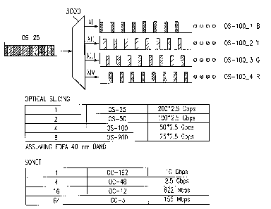
FIGURE 11 depicts the a OS-200 signal being sub-divided into four OS-800
signals;
FIGURE 12 depicts wavelength slot interchange; and
FIGURE 13 depicts a mesh network system.
CA 02376154 2001-12-03
WO 00/76103 PCT/US00/15431
9
DETAILED DESCRIPTION
A WDM signal consists of multiple channels with each channel having its own
range of
wavelengths or frequencies. As used herein, the terms "channel" or "spectral
band" refer to a
particular range of frequencies or wavelengths that define a unique
information signal. Each
channel is usually evenly spaced from adjacent channels, although this is not
necessary. For
example, the wavelength slicers shown in FIGURE 1 can separate channels based
on a 50 GHz
spacing between adjacent channels, as depicted in FIGURE 3. Uneven spacing may
result in
some complexity in design, but, as will be seen, the present invention can be
adapted to such a
channel system. This flexibility is important in that the channel placement is
driven largely by
the technical capabilities of transmitters (i.e., laser diodes) and detectors
and so flexibility is of
significant importance.
The sets of input WDM channels are mutually exclusive, in that there is no
overlap in
the frequency bands assigned to channels in the different sets. In the
preferred embodiment of
the present invention, the first and second sets of channels are
interdigitally spaced as shown in
FIGURE 1. For example, the spacing between adjacent channels in the first set
can be 100
GHz, and the spacing between adjacent channels in the second set can be 100
GHz. The
resulting interdigital spacing between channels after the first and second
sets are combined
would be 50 GHz. This type of arrangement allows for network planning.
Consider the one 50
GHz signal to comprise two 100 GHz signals or four 200 GHz signals. Similarly,
one 25 GHz
signal comprises two 50 GHz signal or comprise four 100 GHz signals or eight
200 GHz
signals or sixteen 400 GHz signals. These signals can be divided as needed to
handle different
situations. Note that other channel configurations could be employed, as long
as there are at
least two mutually exclusive sets of channels. For example, alternating blocks
of channels
could be used to define the first and second sets of channels.
FIGURE 1A is a block diagram illustrating the general functionality of an
individual
wavelength dicer 100 as a component in a larger network system. The input WDM
signal is
coupled using conventional optical signal coupling techniques to the input
port of the
wavelength dicer 100. The wavelength dicer 100 separates the input signal into
two sets of
channels, which are routed to the output ports as depicted in FIGURE 1A.
FIGURE 1B depicts
a 1 x 4 dicer 3000. The input signal is a 25 GHz spaced signal, OS-25, which
is divided into
CA 02376154 2001-12-03
WO 00/76103 PCT/US00/15431
four 100 GHz signals by dicer 3000. Note that each of these signals are
orthogonal to each
other, i.e. they do not overlap. Also note that they are synchronized in the
wavelength domain.
This 1 x 4 dicer can be constructed by cascading two 1 x 2 slicers of FIGURE
1A.
In the preferred embodiment, the wavelength dicer 100 separates alternating
adj acent
5 input channels into the first and second sets of output channels. FIGURE 3
illustrates the
transmission characteristics of a wavelength dicer with a channel spacing of
50 GHz. Each
wavelength dicer 100 is inherently bidirectional, and therefore can be used
interchangeably
either to separate (or demultiplex) an input signal into two sets of output
channels, or to
combine (or multiplex) two sets of input channels into a combined output WDM
signal. Note
10 that no guard bands are needed. Moreover, the system is scalable, e.g. when
a 25 GHz spacing
is available, a 25GHz dicer is attached in front of the 50 GHz dicer and a
second 50 GHz
slicer network may be added to the 25 GHz network. Further note, that by
separating the
adjacent channels, good isolation between adjacent channels is achieved.
FIGURE 2 depicts the details of the structure and operation of one possible
implementation of a wavelength dicer, for other implementations see
"SWITCHABLE
WAVELENGTH ROUTER," U.S. Application Serial Number 08/780,291, filed January
8,
1997, which is hereby incorporated herein by reference.
FIGURE 2 is a detailed schematic diagram of a wavelength dicer 100. Each of
the
optical paths is labeled with either a horizontal double-headed line
indicating horizontal
polarization (p polarization), or a vertical double-headed line indicating
vertical polarization (s
polarization, which may be depicted as "~"), or both horizontal and vertical
double-headed lines
indicating mixed horizontal and vertical polarizations in the optical signal
at that point.
The input signal 101 enters the first birefringent element 102 that spatially
separates
horizontal and vertically polarized components of the input signal. The first
birefringent
element 102 comprises a material that allows the vertically polarized portion
of the optical
signal to pass through without changing course because they are ordinary waves
in the
birefringent element 102. In contrast, horizontally-polarized waves are
redirected at an angle
because of the birefringent walk-off effect. The angle of redirection is a
well-known function
of the particular materials chosen. Examples of materials suitable for
construction of the
birefringent element include calcite, ruble, lithium niobate, YVOa-based
crystals, and the like.
CA 02376154 2001-12-03
WO 00/76103 PCT/US00/15431
11
The horizontally-polarized component travels along a path 201 as an
extraordinary signal in the
first birefringent element 102 while the vertically polarized component 202
travels as an
ordinary signal and passes through without spatial reorientation. The
resulting signals 201 and
202 both carry the full frequency spectrum of the input signal 101.
At least one of the beam components 201 and 202 are coupled to a polarization
rotator
103 which selectively rotates the polarization state of either beam component
201 or 202 by a
predefined amount. In the preferred embodiment, the rotator 103 rotates the
signals by either
0° (i.e., no rotation) or 90°. In FIGURE 2, the vertically-
polarized component 202 is rotated
by 90° so that both signals 203, 204 exiting the polarization rotator
103 have a horizontal
polarization. Again, at this stage, both the horizontal and vertical
components 202, 203 contain
the entire frequency spectrum of channels in the input WDM signal 101.
The stacked waveplates element 104 is a stacked plurality of birefringent
waveplates at
selected orientations that generate two eigen states. The first eigen state
carnes a first set of
channels with the same polarization as the input, and the second eigen state
carries a
complementary set of channels at the orthogonal polarization. The polarization
of the
incoming beam and the two output polarizations form a pair of spectral
responses, where (H,
H) and (V, V) carry the first set of channels from the input spectrum and (H,
V) and (V, H)
carry the complementary (second) set of channels of the input spectrum, where
V and H are
vertical and horizontal polarization, respectively. With horizontal
polarizations 203, 204 input
to the first stacked waveplates element 104 as illustrated in FIGURE 2,
orthogonal vertical and
horizontal polarizations are generated with the first set of channels residing
in horizontal
polarization and the second set of channels residing in vertical polarization.
The pairs of optical responses 205, 206 output by the first stacked waveplates
element
104 are coupled to a second birefringent element 105. This birefringent
element 105 has a
similar construction to the first birefringent element 102 and spatially
separates the
horizontally and vertically polarized components of the input optical signals
205 and 206. The
optical signals 205, 206 are broken into vertically-polarized components 207,
208 containing
the second set of channels and horizontally-polarized components 209, 210
containing the first
set of channels. Due to the birefringent walk-off effect, the two orthogonal
polarizations that
CA 02376154 2001-12-03
WO 00/76103 PCT/US00/15431
12
carry first set of channels 209, 210 in horizontal polarization and second set
of channels 207,
208 in vertical polarization are separated by the second birefringent element
105.
Following the second birefringent element 105, the optical elements on the
input side of
the second birefringent element 105 can be repeated in opposite order, as
illustrated in
FIGURE 2. The second stacked waveplates element 106 has substantially the same
composition as the first stacked waveplates element 104. The horizontally-
polarized beams
209, 210 input to the second stacked waveplates element 106, are further
purified and maintain
their polarization when they exit the second stacked waveplates element 106.
On the other
hand, the vertically-polarized beams 207, 208 experience a 90°
polarization rotation and are
also purified when they exit the second stacked waveplates element 106. The
90° polarization
rotation is due to the fact that the vertically-polarized beams 207, 208 carry
the second set of
channels and are in the complementary state of stacked waveplates element 106.
At the output
of the stacked waveplates element 106, all four beams 21 l, 212 and 213, 214
have horizontal
polarization. However, the spectral bands defined by the filter
characteristics of the stacked
waveplates elements 104, 106 are separated with the second set of channels on
top and the first
set of channels below.
To recombine the spectra of the two sets of beams 21 l, 212 and 213, 214, a
second
polarization rotator 107 and a third birefringent element 108 are used. The
second rotator 107
intercepts at least two of the four parallel beams 211 - 214 and rotates the
polarization of the
beams to produce an orthogonally-polarized pair of beams 215, 216 and 217, 218
for each
spectral band at the output of the second polarization rotator 107. In the
case of FIGURE 2,
the polarization of beams 211 and 213 is rotated by 90°, and beams 212
and 214 are passed
without change of polarization. Finally, a third birefringent element 108
recombines the two
orthogonally-polarized beam pairs 215, 216 and 217, 218 using the walk-off
effect to produce
two sets of channels that exit at the output ports 109 and 110, respectively.
The dicer shown in FIGURE 2 can be used to slice a WDM signal into bands, each
of
which comprises a plurality of wavelength channels, additional dicers would be
used to
separate the bands down to individual channels. This is depicted in FIGURE 4.
FIGURE 4 provides an overall schematic diagram 400 of an embodiment of the
present
invention using two networks 301 and 401 of wavelength dicers. Input WDM
signals 10 from
CA 02376154 2001-12-03
WO 00/76103 PCT/US00/15431
13
an optical link are coupled to the input port of a first wavelength dicer 302.
The input WDM
signal comprises multiple channels with each channel having its own range of
wavelengths or
frequencies.
Each wavelength dicer 302 - 306 in the wavelength dicer network 301 spatially
separates a set of input WDM channels into two complementary sets of output
channels. In the
preferred embodiment, each wavelength dicer separates alternating adjacent
input channels
into first and second sets of output channels as shown in FIGURE 1. The first
wavelength
dicer 302 separates the network input signal 10 into a first set of channels
11 that are routed to
wavelength dicer 303, and a second set of channels 12 that are routed to
wavelength dicer 304.
For example, the initial wavelength dicer 302 can separate channels based on a
50 GHz
spacing between adjacent channels.
The first set of channels output by the initial wavelength dicer 302 is routed
along a
first optical path 11 to second and third stage wavelength dicers 303, 305,
and 306. The
second set of channels output by the initial wavelength dicer 303 is routed
along a second
optical path 12 to wavelength dicer 304. The second state of wavelength dicers
303, 304
further separate the input channels into four sets of channels. For example,
the second state of
wavelength dicers 303, 304 separates channels based on a 100 GHz spacing
between adjacent
channels. This process can be continued by cascading additional stages of
wavelength dicers
to achieve up to 2N sets of channels, where N is the number of stages. For
example, the
wavelength dicer network 301 has a partial third state consisting of
wavelength dicers 305 and
306.
The output channels from wavelength dicer 304 exit the first wavelength dicer
network
301 along optical path 13 without further processing. These output channels
are referred to as
"express lanes" and pass directly to the second wavelength dicer network 401
used to
recombine the optical signals that are to be returned to the optical network,
as will be discussed
below. Optionally, wavelength dicers 304 and 404 could be eliminated so that
the second set
of optical signals from the initial wavelength dicer 302 would serve as the
express lanes and
pass directly to the final wavelength dicer 402 in the second wavelength
slicer network 401.
The first set of channels are further subdivided into four sets of channels
that are
received as inputs by an array of optical filters 307, 308, 309, and 310.
These optical filters
CA 02376154 2001-12-03
WO 00/76103 PCT/US00/15431
14
307 - 310 separate the input sets of channels into an array of separated
channels. The
implementation shown in FIGURE 4 is based on commercially-available
interference filter
arrays that can separate up to eight channels. However, other types of optical
filters can be
employed for spatially separating the channels. The type of optical filter
used and the number
of filters in the array are purely matters of convenience of design. As an
alternative, additional
slicers could be used.
The array of separated channels are connected to the input ports of a series
of
programmable optical add/drop switch arrays 500. Here again, any number of
add/drop switch
arrays can be employed to handle any desired number of channels based on
design
requirement.
Each add/drop switch array 500 also has a corresponding arrays of output
ports, add
ports, and drop ports. The add/drop switch array 500 selectively routes
channels from the input
ports to its drop ports; substitutes channels from the add ports in place of
the dropped channels;
and routes the remaining input channels and the added channels to the output
ports of the
add/drop switch array 500.
The array of output channels from the add/drop switch array 500 passes through
a
regulator 501 which adjustably regulates the optical power level of each
channel. The output
channels are then combined so that they can be transmitted through a second
optical link 15 in
the optical network. The means for combining the output channels consists of a
second array
of interference filters 407 - 410 and a second wavelength slicer network 401.
These devices
are inherently bi-directional, and therefore can be used to multiplex as well
as demultiplex the
WDM signal for the optical network. Each of the interference filters 407 - 410
in the second
array combine eight channels as an inverse operation of that performed by the
first array of
interference filters 307-310. The second array of interference filters 407-410
also serve to
purity the spectral characteristics of the output channels and reduce cross-
talk. Wavelength
dicers 405, 406, and 403 in the second wavelength dicer network 401 multiplex
the sets of
channels from the second array of interference filters 407 - 410 as an inverse
operation to the
demultiplexing provided by wavelength dicers 303, 305, and 306 in the first
wavelength dicer
network 301. Similarly, wavelength dicers 404 and 402 combine the express
lanes 13 with the
CA 02376154 2001-12-03
WO 00/76103 PCT/US00/15431
multiplexed channels from the wavelength slicer 403 to reconstitute the entire
WDM signal for
the optical network.
It should be understood that other means could be readily substituted to
combine output
channels from the add/drop switch arrays 500 and the express lanes 13 since
each channel has a
unique wavelength.
FIGURE 5 depicts an add/drop smart switch 590 for use in the switch array 500.
The
array would be comprised of 32 switches 590, each of which can be individually
controlled to
selectively replace one of the input channels with one of the add channels.
The smart switch
590 is described more fully in Attorney Docket Number 55872-P043CP1-993120,
entitled
10 "FIBER OPTIC SMART SWITCH," which is hereby incorporated herein by
reference.
The smart switch 590 includes a polarization beam sputter 502 which is shown
in
Attorney Docket Number 555872-P048US-992837, entitled "HIGH EXTINCTION RATIO
POLARIZATION BEAMSPLITTER," which is hereby incorporated herein by reference.
The
beamsplitter 502 operates to pass p light (horizontal or "~") through the
beamsplitting surfaces,
15 and deflects s light (vertical or "~"). Thus, when the input 503 and the
add 504 signals are in p
light, the input 503 signal is routed to the drop port 506 and the add 504
signal is routed to the
output port 505. This mode is known as the add/drop mode. When the input 503
is s light, the
input 503 signal is routed to the output port 505. This mode is known as the
bypass or pass
through mode. Note that in this mode there is no add signal. To properly
process the signals,
the switch 590 includes a collimator 507 to collimate the input/add light,
birefringent separator
elements 508 to separate the light into its p and s components and to
laterally displace the p
and s components.
The birefringent element 508 is made of a material that allows the vertically
polarized
portion of the optical signal to pass through without changing course because
they are ordinary
waves in the birefringent element 508. In contrast, horizontally polarized
waves are redirected
at an angle because of the birefringent walk-off effect. The angle of
redirection is a well-
known function of the particular materials chosen. Examples of materials
suitable for
construction of the birefringent elements used in the preferred embodiments
include calcite,
ruble, lithium niobate, YV04 based crystals, and the like.
CA 02376154 2001-12-03
WO 00/76103 PCT/US00/15431
16
The switch also uses a halfwave plate 509 to change one of the polarization
components into the other component, (as shown, the plate changes the s
component into p
light, however it could be placed in front of the p component) and thus all of
the light incident
onto the rotator is of the same polarization type. Each output/drop port
includes a reverse of
the input elements. Note that the halfwave plate on the output port is on the
opposite branch
from plate 509. This provides balance to the system by having the light from
each branch pass
through the same number of optical elements. Also, note that since the smart
switch 590
performs regulation, the additional regulator 501 is not needed.
The PBS 502 is surrounded by four polarization controllers or rotators 510.
The
rotators 510 are used to control the polarization of the light received by the
PBS . The voltage
applied to the rotators causes the light to either pass through unrotated ( 15
volts) or rotated
such that p becomes s and s becomes p (0 volts). For example, if the light
incident onto the
PBS is made to be p light, the light will pass through the PBS, and if the
light is made to be s
light, the light will be deflected by the PBS. The switchable polarization
rotators 510, 514, 515
can be made of one or more types of known elements including parallel aligned
liquid crystal
rotators, twisted pneumatic liquid crystal rotators, ferro electric liquid
crystal rotators, pi-cell
liquid crystal rotators, magneto-optic based Faraday rotators, acousto-optic
and electro-optic
polarization rotators. Commercially available rotators using liquid crystal
based technology
are preferred.
The switch 590 includes a partially reflecting mirror 511 which passes about
95% of
the incident light, and deflects about 5% of the light. The deflected 5% is
indecent onto a
detector 512 which measures the amount of light. The controller electronics
513 uses this
measurement to control the rotators, as shown input rotator 514 and output
rotator 515. Note
that the voltage being applied to the rotators can be varied between 0-15
volts, the voltage level
determines how much of the light is rotated.
By controlling the voltage level to the input rotator 514, the add/drop switch
can have a
drop and continue operation. For example, if the rotator 514 changes both
branches of the
input signal to half p and half s, then half of the input signal will be
routed to the drop port 506,
and half of the input signal will be routed to the output port 505. This
operation allows for the
input signal to be split, and thus shared between two network components. The
operation also
CA 02376154 2001-12-03
WO 00/76103 PCT/US00/15431
17
allows for the regulation/attenuation of the output signal 505 by shunting a
portion of the input
signal to the drop port. This prevents the output signal 505 from this switch
to be greater than
output signals from other switches in the array 500. The add signal can be
similarly controlled.
Note that by controlling the output rotator 515, the output signal can also be
controlled in such
a manner.
As shown in FIGURE 5, the input signal is split into two components during
processing, and recombined by a birefringent element S 16 prior to outputting.
The output
rotator 515 can introduce both p and s polarizations into each branch of the
signal. Normally,
the vertical branch 517 passes through the element, and thus the output
collection point 519 is
located along this path. The horizontal branch 518 is deflected into the path
of the vertical
branch 517 for collection. However, if the vertical branch 517 has been
changed to include a
horizontal component, then this component is deflected out of the element and
away from the
collection point 519. Similarly, if the horizontal branch 518 has been changed
to include a
vertical component, then this component will pass through the element and away
from the
collection point 519. Thus, this rotator SOS will provide for
regulation/attenuation of the
output signal. The drop signal can be similarly controlled.
The array of add/drop switches can be formed in matrix arrangement to allow
for
interconnection or cross-connection of the add and drop ports. FIGURE 6
depicts a 4 x 4 array
1000 of PBSs 700. In front of each input path to each respective PBS is a
polarization
controller (not shown) which controls the polarization of the light entering
the respective PBS,
i.e., the controller could change the light such that the light incident onto
the PBS is p light or s
light. In the add/drop mode, where the input goes to drop, and the add goes to
output, each of
the add signals, ABCD, would go to a respective output path, 5678. Similarly,
each input
signal, EFGH, would go to a respective drop path, 1234. The add/drop mode is
accomplished
by setting the various rotators to emit only p light.
In the bypass mode, each input signal, EFGH, could be directed to any one of
the
outputs paths 5678. Thus, inputs EFGH could be outputted to 5768, 5867, etc.
The bypass
mode is accomplished by setting particular ones of the rotators to s light.
For example, to have
the E input switched to output 6, the input rotator for unit 1001 would be set
to provide s light
to the unit. The other units in the E input column would be set to provide p
light such that the
CA 02376154 2001-12-03
WO 00/76103 PCT/US00/15431
18
light would pass through the PBSs, until encountering unit 1001. The output
rotator from 1001
would be set to provide p light such that the light passes through the units
of the output 6 row,
and consequently be delivered to output 6. Thus, the various rotators are used
to control the
polarization of the light that is incident onto the various PBSs of the switch
module, and thus
control their connection.
Note that various combinations of the switch and pass through states can be
achieved.
For example, input E could be routed to drop, inputs FGH could be routed to
outputs 567,
respectively, and add D could be routed to output 8. As general rules, input E
can be routed to
any of 15678, input F can be routed to any of 25678, input G can be routed to
any of 35678,
input H can be routed to any of 45678, while input A can be routed to 5, input
B can be routed
to 6, input C can be routed to 7, and input D can be routed to 8. Note that
the 4 x 4
arrangement is by way of example only, as the PBS can be arranged in a N x M
array, see "N x
M DIGITALLY PROGRAMMABLE OPTICAL ROUTING SWITCH USING HIGH
EXTINCTION RATIO POLARIZATION BEAM SPUTTER," Attorney Docket Number
55872-P046CP1CP1-993118, which is incorporated herein by reference. The switch
described
above is actually more than 4 x 4, as defined by the conventional definition.
It has a total of 16
ports, 4 input and 4 output ports are cross connected. The other set of 4/4
input/output ports
are used for add/drop operation. This feature is not available in the prior
art. Note that each of
the switches in the array may be a smart switch, and thus have its respective
rotators controlled
by varying the applied voltage based on the output (or drop) light.
FIGURE 7 depicts an arbitrary add/drop switch 1100. This switch is comprised
of two
4 x4 modules of FIGURE 6, note that only one set of input/output elements are
needed. This
arrangement permits any input signal ABCD to be dropped to any drop path 1234.
Similarly
any add signal EFGH can be delivered to any output path 5678. Also the input
signals ABCD
can be passed through to their respective output paths 5678. Again, each of
the switches in the
array may be a smart switch, and thus have its respective rotators controlled
by varying the
applied voltage based on the output (or drop) light. This arrangement allows
for a mesh type
connection, as shown in FIGURE 13, and thus is useable with Internet protocol
(IP).
Consequently, IP protocol data can be routed over WDM. Also, as demonstrated
by FIGURE
4, different amounts of bandwidth can be allocated to different areas. For
example, if the local
area needs more bandwidth, then the express lanes could be routed into the
local area. If less
CA 02376154 2001-12-03
WO 00/76103 PCT/US00/15431
19
bandwidth is needed, then more express lanes could be created. This is shown
in FIGURE 13
by the different thickness of lines, including higher bandwidths (or smaller
signal spacing, e.g.
SOGHz) and numbers of lines (numbers of fibers).
FIGURE 8 depicts the arbitrary add/drop switch of FIGURE 7 with wavelength
conversion. In addition to operations described in FIGURE 7, each input signal
7~1, 7~2, 7~3, ~,4,
can be routed to any of the detectors 1101, where each signal is converted
into an electrical
signal and processed by electronics 1102. The output electrical signal are
then sent to
respective lasers 1103 for retransmission as light. Each light output from the
lasers can be
routed to any of the output paths. Again, each of the switches in the array
may be a smart
switch, and thus have its respective rotators controlled by varying the
applied voltage based on
the output (or drop) light.
Each of the types of add/drop switches would provide the network of FIGURE 4
with
different operating capabilities. Note that other add/drop switches as
described in Attorney
Docket Number 555872-P042CP2CP1-993119, entitled "OPTICAL ADD/DROP
WAVELENGTH SWITCH USING A HIGH EXTINCTION RATIO POLARIZATION
BEAMSPLITTER," which is incorporated herein by reference, could be used herein
as array
500.
Also note that the network of FIGURE 4 could be protected according to the
fault
handling mechanisms described in U.S. Application Serial Number 09/190,078,
entitled
"SYSTEM FOR DEALING WITH FAULTS IN AN OPTICAL LINK," filed November 12,
1998, which is incorporated herein by reference. This type of OS protection is
useful for
handling IP protocol data. Layer 3 protection is provided by the Internet
protocol.
FIGURE 9 depicts a drop/add switch for wavelength management and restoration.
Note that FIGURE 9 includes four fibers 1201, and four 4 x 4 modules 1203.
Note that the
number of fibers is by way of example only, as more fibers would merely
require a scaled
drop/add switch. Also note that the modules are shown as being only partially
connected to
DEMUXes and MUXes to simplify the figure. Further note that ~,1, 7~2, ~,3, and
~,4, can be
viewed as ~,b (blue), ~,g (green), ~,y (yellow), and ~,r (red). Each fiber
carries different signals
which are encoded by wavelength, e.g. 7~1, ~,2, 7~3, ~,4. These signals are
demultiplexed by
DEMUR 1202. Each wavelength from each fiber is provided to a particular 4 x 4
module, e.g.
CA 02376154 2001-12-03
WO 00/76103 PCT/US00/15431
7~1 from each of the four fibers is provided to module 1203. Within each
module 1203, the
operations are as described with respect to FIGURE 6. Thus, particular signals
can be dropped
or added or re-routed to the output. Note that the diagonal slash through each
module indicates
the orientation of the PBSs within the module. For a further discussion on
multiple
5 wavelength management, see related application "MLTLTI-WAVELENGTH CROSS
CONNECT OPTICAL NETWORK," Application Serial Number 08/907,551, which is
incorporated herein by reference.
FIGURE 10 depicts a mufti-ring network system 2000 connecting seven nodes A,
B, C,
D, E, F, and G. Note that the ring connecting DEFG is connected by an OS-200-4
line, while
10 another OS-200-4 line ring connects ADC, without connecting B. The ABC ring
is connected
by an OS-200-2 line. The OS-200-1 ring connects ABCD, and OS-200-3 ring
connects nodes
BCD. The various switches described above allow this network to have express
connections,
to perform local add/drops of signals. For example, node E could comprise a
the switch shown
in FIGURE 6, where the OS-200 is sliced down to four OS-800 signals and can
perform
15 add/drops to those signals. Node D could comprise the wavelength cross-
connect switch
shown in FIGURE 9 to cross-connect the OS-200-4 fibers. As shown in FIGURE 11,
each
OS-200-4 signals can be divided into four OS-800 signals. Note that FIGURE 9
would be
simplified in this case, as it would have four 4 x4 switches with two input
DEMUXs. The two
OS-200-4 fibers would be inputted into the input DEMUXs, and processed into
the switches
20 from there, an OS-800 signal from one of the fibers can be connected into
the other input line,
or other signals can be added into the lines, etc.
As shown in FIGURE 12 a cross-connected node, such as node D in FIGURE 10,
empty slots can be filled via wavelength slot interchange. For example, train
4000 has empty
slots 4001, 4002. These may be filled via a add/drop switch with wavelength
conversion as
shown in FIGURE 8. In other words, a signal can have its wavelength changed,
and be added
into an empty slot. Also the wavelength cross-connect switch shown in FIGURE 9
can be used
to move a signal with the same wavelenght from a different train in the empty
slot.
The above disclosure sets forth a number of embodiments of the present
invention.
Other arrangements or embodiments, not precisely set forth, could be practiced
under the
teachings of the present invention and as set forth in the following claims.
CA 02376154 2001-12-03
WO 00/76103 PCT/US00/15431
21
Other types of frequency multiplexers and demultiplexers could be readily
substituted
in place of the wavelength slicers 101-104 shown in FIGURES 1-3. For example,
a set of
polarization rotators and a polarized beamsplitter can be used to combine the
first and second
sets of channels, in place of wavelength dicers 1 O1 and 102 in terminal 1.
Demultiplexing can
S be accomplished by filters or diffraction gratings, although such approaches
would tend to be
less efficient and more expensive.
Although the present invention and its advantages have been described in
detail, it
should be understood that various changes, substitutions and alterations can
be made herein
without departing from the spirit and scope of the invention as defined by the
appended claims.
Moreover, the scope of the present application is not intended to be limited
to the particular
embodiments of the process, machine, manufacture, composition of matter,
means, methods
and steps described in the specification. As one of ordinary skill in the art
will readily
appreciate from the disclosure of the present invention, processes, machines,
manufacture,
compositions of matter, means, methods, or steps, presently existing or later
to be developed
that perform substantially the same function or achieve substantially the same
result as the
corresponding embodiments described herein may be utilized according to the
present
invention. Accordingly, the appended claims are intended to include within
their scope such
processes, machines, manufacture, compositions of matter, means, methods, or
steps.