Note: Descriptions are shown in the official language in which they were submitted.
CA 02376185 2001-12-03
WO 00/77802 PCT/US00/16018
-1-
CHARGE TRANSFER APPARATUS AND METHOD THEREFORE
BACKGROUND OF THE INVENTION
Field of the Invention:
The present invention relates generally to the field of electric power
conversion, and, more particularly, to a charge-transfer apparatus and method
for
alternating-current to alternating-current (AC-to-AC) power conversion,
alternating-
current to direct-current (AC-to-DC) rectification, DC-to-AC inversion, DC-DC
power conversion, and volt-ampere-reactive (VAR) control. Although the
invention is
subject to a wide range of applications, it is especially suited for use in
power
distribution and transmission systems in electric utility, industrial,
commercial, and
marine applications.
Description of the Related Art:
Standard AC-to-DC rectification apparatus using non-linear devices, for
example, diode or thyristor bridges, causes harmonics and reactive power on a
three-
phase AC power supply providing electrical power to the apparatus. The
harmonics
and reactive power are caused by the uneven loading of the input phases. That
is,
current is drawn from the phase when the input AC phase voltage is greater
than the
output DC voltage, and no current is drawn from a phase when the input AC
phase
voltage is less than the output DC voltage.
With the proliferation of variable-speed motor drives and back-up power
sources, which typically require an AC-to-DC then DC-to-AC conversion to
obtain the
desired AC motor voltage and frequency, further distortion of the waveform of
the AC
power supply arises. As the waveform of the power supply, such as, the
electric utility
CA 02376185 2001-12-03
WO 00/77802 PCT/US00/16018
-2-
grid a generator on a marine vessel, deteriorates, malfunctions can occur to
equipment
that depend on a "clean" source of power for proper operation.
A need therefore exists for a power conversion apparatus, and a method
therefore, that reduces distortion of the waveform of the AC power supply.
BRIEF SUMMARY OF THE INVENTION
The present invention, which tends to address this need, resides in a resonant
charge-transfer apparatus (RCTA), and differential and sequential resonant
charge-
interchange (DSCI) method therefore. The RCTA and DSCI method described herein
provides advantages over known power-conversion apparatus in that it reduces
distortion of the waveform of the AC power supply, among other things.
The RCTA reduces this problem by drawing charge from all phases of a multi-
phase power supply in proportion to the ratio of the current of the input
phases. This
yields harmonic-free power, draws power at unity power factor, and does not
introduce reactive power into the AC power supply.
Furthermore, because the RCTA can be bi-directional, it can inject harmonic-
free current at the fundamental frequency into the multi-phase AC power supply
as
well as synthesize a sinusoidal current waveform with a desired frequency and
phase.
In general terms, the RCTA operates in two cycles. First, a desired charge is
drawn from each phase of a power supply to charge an energy storage device.
Second, the charge on the energy storage device is discharged through the
output of
the RCTA. Through many cycles of operation per second, the RCTA can extract
charge from the power source and inject the charge through the output of the
RCTA
to construct a desired output waveform.
These transfers of charges may or may not provide a net energy transfer to or
from the input terminal. With repeated charge interchanges, a net and
controlled
power flow can occur from an input terminal to an output terminal; or the
repeated
charge interchange can provide controlled reactive power of an AC power
supply.
CA 02376185 2001-12-03
WO 00/77802 PCT/USOO/16018
-3-
The power applied to the RCTA may be either multi-phase AC or DC. The
produced output waveform can be either multi-phase AC having a desired voltage
and
frequency or DC having a desired voltage level and polarity. Conversion can be
from
AC to AC or DC, and DC to AC or DC.
For power flow control, the charge interchange occurs, in most applications,
by
a charge interchange between the power source and the charge storage device
followed by a charge interchange between the charge storage device and the
output.
However, a direct power flow between the input terminal and the output
terminal can
be accomplished.
By controlling the charge interchange process, current can be drawn from, or
injected into, a terminal; and, if averaged with a low-pass filter, yield
practically ripple-
free current flow.
An advantage of this invention is that it can utilize high-power thyristors
that
operate in a self or natural commutation mode. Thus, it does not require
opening
switches, such as, the pulse-width modulator (PWM) inverters using insulated-
gate
bipolar transistors or gate turn-off devices. Consequently, a circuit to
control the
opening of switches is not required.
The invention can use conventional thyristors, which have been in use for
about
30 years. Unlike many conventional power electronic circuits, the power
electric
components utilized in the present invention are available and need not be
developed.
Also, these devices have the highest voltage rating, highest current rating,
and one of
the lowest forward voltage drops of any power electronic switch. These devices
also
have low losses, are inexpensive, and are available with both high-voltage and
high-
current ratings. Thus, the RCTA can be scaled up with present technology for
high-
power and high-voltage applications.
There are many applications for the RCTA and DSCI method. For example,
the RCTA can be utilized in an AC-to-AC converter with power transfer
occurring
without the typical intermediate DC link. It can also be utilized as an AC-to-
DC
CA 02376185 2001-12-03
WO 00/77802 PCT/US00/16018
-4-
rectifier, DC-to-AC inverter, DC-to-DC converter, multi-port converter,
harmonic
compensator, VAR compensator, and electronic transformer,.
A feature of the RCTA is the harmonic-free conversion of multi-phase AC
power to either multi-phase AC or DC. This is achieved by extracting charge
from all
of the phases in proportion to ratio of the current of the input phases by
differentially
charging the charge storage device from two input phases, followed by the
replacement of one of the two phases by a third phase (referred to as
"differential and
sequential resonant charge-interchange (DSCI)").
Performing the charging at controlled intervals loads the multi-phase AC power
supply to the desired power level at any part of the AC cycle. Loading the
multi-phase
AC power supply uniformly maintains a balanced and constant power. Through
controlled charging, current can be drawn from the input that is in phase with
the input
voltage, thus the input power has a unity power factor. This eliminates the
requirement for phase-angle corrections or VAR capacitors at the input of the
RCTA.
This technique is not restricted to a three-phase AC power system, but may be
extended to any multi-phase system.
Through controlled discharging, the AC-to-AC converter can synthesize the
output frequency and phase.
Further, the AC-to-AC converter can transfer energy from the AC power
supply to an AC terminal that has its frequency and phase determined by
another AC
power source, such as, a generator. The injected charge can be in phase with
the
voltage of the another AC power source to transfer real AC power. Or, the
injected
charge can contain a fraction of charge that is out of phase with the voltage
of the
another AC power source, such that the power transfer contains reactive power.
This
mode of operation permits controlled power transfer from one AC power source
to
another AC power that have different phase, voltage, and frequency.
An application of the AC-to-AC converter is the controlled operation of power
transfer between systems of different voltages. This permits controlled power
flow to
CA 02376185 2001-12-03
WO 00/77802 PCT/US00/16018
-5-
a system that may experience voltage, phase, and frequency instability. For
example,
the AC-to-AC converter may be used on the electric utility grid as a gateway
controller
to control the desired power flow. The gateway controller can control the
power flow
through an AC transmission line and limit the power flow within the thermal
limit of
the transmission lines. The gateway controller can also be used to transfer
power from
one regional AC power system to an adjoining AC power system. This could
replace
the utilization of DC link between the Easter, Western, the Texas, the
Mexican, and
the Canadian regional grids.
In another application, the gateway controller can control the power flow to
damp the sub-harmonic instability of a regional AC grid.
Another application of the AC-to-AC converter is convert the frequency of the
AC power supply to a different output frequency. This feature has many
applications,
one being for the use of variable speed motor drives. The AC-to-AC converter
can
dynamically control the voltage, frequency, phase, real power, and reactive
power to
the motor on a continuous basis over a specified range. Since the AC-to-AC
converter
can be controlled for bi-directional power flow, the motor can be also
controlled for
dynamic braking for full four-quadrant operation.
In another application, with a single-phase transformer inserted into either
the
charge or discharge cycle, the RCTA can be an electronic transformer with
output
voltage regulation, frequency change, and phase control capabilities. The
input and
output may be either DC or AC.
The single-phase transformer provides a greater input-to-output voltage ratio
change over a large range than the previously described AC-to-AC power
converter.
The single-phase transformer can be used to step-up or step-down the input
voltage.
Further, the single-phase transformer can be used to obtain full galvanic
isolation
between the input and output. Because the single-phase transformer is located
in the
high frequency section of the electronic converter, the magnetic core size can
be
reduced.
Further, a typical AC transformer is energized all the time independent of the
load factor, significantly reducing the efficiency at low and average loads.
In the
CA 02376185 2001-12-03
WO 00/77802 PCTIUSOO/16018
-6-
present invention, the efficiency is relatively constant because the core of
the
transformer is only energized when throughput power is required.
The transformer may be part of the charging circuit, inserted between the
input
switches and the charge storage device, or part of the discharge circuit,
inserted
between the charge storage device and the output switches.
Insertion of a single-phase transformer permits the RCTA to be utilized as a
regulated electronic transformer. When an AC power supply for a facility needs
to be
stepped down in voltage, the electronic transformer not only performs the
voltage
transformation, output voltage regulation, and VAR neutralization, but also
acts as the
electronic circuit breaker, eliminating the need for mechanical switchgear.
Another application for the electronic transformer is as an interface between
an
AC power source and the AC grid. The power can be stepped-up from the
generator
voltage to the transmission voltage. Because the generator does not have to
operate at
the AC grid power frequency, a much greater flexibility is obtained. For
example, the
power source may be a turbine, a wind power generator, or an hydroelectric
power
plant. It is well known that a significantly higher fraction of the power can
be captured
for both the wind and hydroelectric power plant if the generator is not forced
to
operate at a constant frequency.
Still other implementations of the electronic transformer is an AC-to-DC step-
down configuration for DC industrial processes, and an AC-to-DC step-up of the
output of an AC generator to DC for direct DC transmission.
Using the DSCI technique for AC-to-DC power rectification, the power
throughput can be fully regulated to yield a highly regulated output with
minimum DC
output-voltage ripple. The energy in the charge storage device is resonantly
discharged into the DC output terminal.
In a preferred embodiment, a three-phase AC power supply is applied to the
input terminal of the RCTA and a DC output that is positive, negative, or bi-
polar is
outputted. Unlike standard bridge rectification technique, no transformer
isolation is
CA 02376185 2001-12-03
WO 00/77802 PCT/US00/16018
-7-
required for a grounded system. In addition, several rectification modules may
be
operated in parallel with full individual power throughput control.
A feature of the AC-to-DC rectifier is that the output polarity can be
operated
over a large DC-voltage range with nearly instantaneous polarity reversal.
Unlike the
standard rectification process, where the output voltage is limited to a
maximum value
depending on the AC-input voltage, for this invention the output can be
significantly
boosted, only being limited by the selection of the active and passive
components. The
boost capability implies that, for many operations, standard voltages can be
used
eliminating transformers, and also a constant output can be maintained even
with a
significant droop of the AC power source. The droop can be either on the order
of a
cycle or over a prolonged period of time.
Several modes of voltage regulations are possible, for example, but not
limited
to, the following:
a. Pulsed density modulation, by increasing or decreasing the
number of charge and discharge cycles per a selected time interval.
b. Residual voltage regulation of the charge storage device,
typically controlled as part of the discharge cycle of the charge storage
device.
c. Control of the charging energy of the charge storage device
during the charging cycle.
d. Control of the discharge energy of the charge storage device
during the discharging cycle.
An important feature of all regulation options is that the majority of the
regulation does not require opening switches and falls under the category of
"soft
switching" operation.
The RCTA can also be utilized in a DC-to-AC inverter by reversing the AC-to-
DC operation. The DC-to-AC inverter retains all the benefits that have been
given
above for the AC-to-DC converter.
CA 02376185 2007-07-27
69675-614
-7a-
According to one aspect of the present invention,
there is provided a method of transferring electric charge
between a charge storage device and a first power terminal
having a plurality of first-nodes, said method comprising:
interchanging charge between the charge storage device and a
first first-node of the plurality of first-nodes through an
inductive section; when a selected charge has been
interchanged between the charge storage device and the first
first-node, generating a control signal that causes an
electrical switching from the first first-node to a second
first-node of the plurality of first-nodes; and then
interchanging charge between the charge storage device and
the second first-node through the inductive section.
According to another aspect of the present
invention, there is provided a charge transfer apparatus
comprising: an inductive section; a charge storage device
coupled with the inductive section to form a resonant
circuit with the inductive section; a first power terminal
having a plurality of first nodes; a plurality of first
switches coupling the first power terminal with the resonant
circuit; and a control unit for controlling the operation of
the plurality of first switches to interchange charge
between the charge storage device and a first first-node of
the plurality of first nodes through the inductive section
and when a selected charge has been interchanged between the
charge storage device and the first first-node, generating a
control signal that causes the plurality of first switches
to switch from the first first-node to a second first-node
of the plurality of first-nodes, and then interchange charge
between the charge storage device and the second first-node
through the inductive section.
CA 02376185 2008-07-23
69675-614
-7b-
According to another aspect, there is provided a
method of transferring electric charge between a charge
storage device and a first power terminal having a plurality
of first-nodes, said method comprising: interchanging charge
between the charge storage device and a first first-node of
the plurality of first-nodes through an inductive section;
when a predetermined charge has been interchanged between
the charge storage device and the first first-node,
replacing the first first-nodes by a second first-node of
the plurality of first-nodes; and interchanging charge
between the charge storage device and the second first-node
through the inductive section.
In one embodiment, wherein a second power terminal
has a plurality of second-nodes, the method further
comprises: interchanging charge between the charge storage
device and a first second-node of the plurality of second-
nodes through the inductive section; when a predetermined
charge has been interchanged between the charge storage
device and the first second-node replacing the first second-
node by a second second-node of the plurality of second-
nodes; and interchanging charge between the charge storage
device and the second second-node through the inductive
section.
In another embodiment there is provided a charge
transfer apparatus comprising: an inductive section; a
charge storage device coupled with the inductive section to
form a resonant circuit with the inductive section; a first
power terminal having a plurality of first nodes; a
plurality of first switches coupling the first power
terminal with the resonant circuit; and a control unit for
controlling the operation of the plurality of first switches
to interchange a first predetermined amount of charge
between a first node of the plurality of first nodes and the
CA 02376185 2008-07-23
69675-614
-7c-
energy storage element and to interchange a second
predetermined amount of charge between a second node of the
plurality of first nodes and the energy storage element,
wherein the ratio of the first predetermined amount of
charge interchanged between the charge storage device and
the first node and the second predetermined amount of charge
interchanged between the charge storage device and second
node is equal to a ratio of the currents drawn from the
first node and the second node.
CA 02376185 2001-12-03
WO 00/77802 PCT/US00/16018
-8-
The DC-to-AC inverter can synthesize an AC power source with a controlled
voltage amplitude, constant or variable frequency, and selected phase angle.
Or,
energy can be transferred from the DC power source to an AC terminal that has
its
frequency and phase determined by an AC power source. The DC-to-AC inverter
can
simultaneously deliver not only the real power, with the injected current
being in phase
with the voltage, but also generate simultaneously reactive power with the
current
either leading or lagging the AC voltage wave form.
One application that takes advantage of the dual modes of AC-to-DC
rectification and DC-to-AC inversion is energy storage in a battery. Energy
can be
extracted from the AC input during AC power availability on an electric grid,
and the
stored energy can returned to the AC grid when power is required.
Another application is for use with variable speed motors. The DC-to-AC
operation can supply both the real and reactive power demand of the motor. The
AC-
to-DC operation would be applicable during the controlled dynamic breaking
with the
inverter delivering the real power to the DC power source.
The RCTA can be used to connect more than two power terminals to the
charge storage device to form a multi-port inverter. All of these ports may be
configured to have bi-directional power flow and the ports can be combinations
of AC
or DC, permitting transfer of electric charge or energy from any of the ports
to any
other port. Integrated into such a multi-port inverter can be a transformer.
This
would permit the connection of power terminals that are at different voltage
levels.
The multi-port inverter has a large number of practical applications. Two
input AC
power buses may be used to provide a redundant power source. Or a similar
three-
port configuration can be combined with a charge storage device to yield an
uninterruptable power supply.
The RCTA can be utilized as a static volt-ampere-reactive (VAR) controller,
harmonic compensator, voltage regulator, or flicker controller.
CA 02376185 2001-12-03
WO 00/77802 PCT/US00/16018
-9-
Other features and advantages of the present invention will be set forth in
part
in the description which follows and accompanying drawings, and in part become
apparent to those skilled in the art upon examination of the following
detailed
description taken in conjunction with the accompanying drawings, or may be
learned
by practice of the present invention. The advantages of the present invention
may be
realized and attained by means of the instrumentalities and combinations
particularly
pointed out in the appended claims.
BRIEF DESCRIPTION OF THE DRAWINGS
FIG. 1 is an electrical schematic of a power converter with frequency changer
and bi-directional power flow capability;
FIG. 2 is a graph of a typical charge interchange waveform of the power
converter, shown in FIG. 1, operating at unity input and output power factor;
FIG. 3 is a graph of another typical charge interchange waveform of the
converter, shown in FIG. 1, operating at unity input power factor and
supplying
reactive power and voltage boost;
FIG. 4 is an electrical schematic of the basic architecture of a DC-to-DC
converter with bi-directional power flow capability;
FIG. 5 is block diagram of a multi-port converter with AC and DC inputs and
AC and DC outputs;
FIG. 6 is an electrical schematic of another embodiment of a power converter
with simultaneous input and output operation;
FIG. 7 is an electrical schematic of a dynamic VAR compensator;
FIG. 8 is a graph of a typical charge interchange waveform of the dynamic
VAR compensator, shown in FIG. 7, with two cycles of operation;
FIG. 9 is an electrical schematic of an electronic transformer that combines
frequency control with voltage transformation;
CA 02376185 2001-12-03
WO 00/77802 PCT/US00/16018
-10-
FIG. 10 is an electrical schematic of electronic transformer with simultaneous
input and output operation;
FIG. 11 is an electrical schematic of power converter using three capacitors;
FIG. 12 is a graph of the capacitor voltages and charge currents for the power
converter using three capacitors, shown in FIG. 11, for a typical charging
process;
FIG. 13 is a graph of several cycles of the voltage and current inputs for the
power converter shown in FIG. 11;
FIG. 14 is a graph of the output voltage over several AC cycles of the power
converter shown in FIG. 11;
FIG. 15 shows the capacitor voltages and charge currents for the power
converter with three capacitors, shown in FIG. 11, for a typical charging
process with
a residual voltage in the capacitors;
FIG. 16 is an electrical schematic of still another embodiment of a power
converter with three capacitors;
FIG. 17 is a graph of a set of parametric operating curves of the real power
flow as a function of the residual voltage phase angle for the power converter
with
three capacitors shown in FIGs. 11 and 16;
FIG. 18 is a graph of a set of parametric operating curves of the reactive
power
flow as a function of the residual voltage phase angle for the power converter
with
three capacitors shown in FIGs. 11 and 16;
FIG. 19 is a graph of a set of parametric operating curves for the input power
flow control given the reactive power as a function of the real power flow
angle for the
power converter with three capacitors shown in FIGs. 11 and 16;
CA 02376185 2009-11-17
69675-614
-11-
FIG. 20 is a graph of a set of parametric operating curves for the output
power
flow control given the reactive power as a function of the real power flow
angle for the
power converter with three capacitors shown in FIGS. 11 and 16;
FIG. 21 is an electrical schematic of the basic architecture of a power
converter
output section with the addition of commutation inductors to reduce the
current rate of
change of the commutation switches.
DESCRIPTION OF THE PREFERRED EMBODIMENTS
1. AC-to-AC Power Converter
a. Circuit
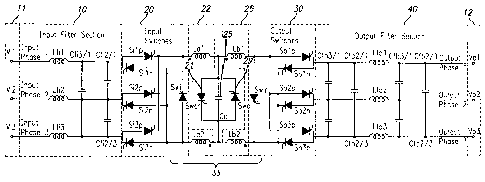
FIG. I illustrates an electrical schematic of one embodiment of the
RCTA employed as an AC-to-AC power converter 5 with frequency changer and bi-
directional power flow capability. The AC-to-AC power converter exemplifies
the
basic structure and operation of the RCTA and DSCI method and will be
described
first. There are several embodiments of the RCTA and DSCI method, but the
basic
structure and operation of each is the same or similar.
The AC-to-AC converter can be directly connected to the AC grid without the
use of a transformer. This will eliminate transformer losses and the cost,
volume, and
weight requirements of a transformer. Obviously, a transformer can be used if
a
specific apparatus is designed and constructed to require a different input
voltage.
AC-to-AC converter 5 comprises a three-phase input terminal 11 for receiving
a three-phase AC power supply, a three-phase low-pass input filter 10, an
input switch
section 20, an input inductive section 22, a charge storage device 25, an
output
inductive section 26, an output switch section 30, a three-phase low-pass
output filter
40, and a three-phase output terminal 12 for supplying an output voltage.
Input filter 10 reduces the current ripple to a negligible value. Further, the
filtering of high frequencies reduces both the filter capacitor and inductor
values.
Input filter 10 comprises inductors Lfil, Lfi2, and Lfi3 and capacitors
Cfi3/1, Cfi2/l,
and Cfi2/3 in an "L-C" or "delta" configuration. A "Y" configuration could be
used as
CA 02376185 2001-12-03
WO 00/77802 PCT/US00/16018
-12-
well. With a switching frequency around 2000 Hz, a cut-off frequency of about
600
Hz is selected for the low-pass input filter.
Input switch section 20 controls the charging of charge storage device 25 from
the phases of the three-phase power supply. Input switch section 20 comprises
six
input switches (Silp, Siln, Si2p, Si2n, Si3p, and Si3n), two switches of
opposite
polarity for each input phase. The input switches can be conventional
thyristors.
Input inductive section 22 is one part of a resonant charge circuit formed
with
charge storage device 25. Input inductive section 22 includes two coupled
inductors
Lal and La2. Lal is coupled in series between the three positive input
switches (Silp,
Si2p, and Si3p) and charge storage device 25; and La2 is coupled in series
between the
three negative input switches (Siln, Si2n, and Si3n) and charge storage device
25.
Only one charging inductor can be used, but, for symmetry, two are shown.
The charge storage device 25 stores the charge from the input phases and
discharges the stored charge to output terminal 12. In this embodiment, charge
storage device 25 includes a capacitor Co coupled in series with inductors Lal
and
La2.
Output inductive section 26 is one part of a resonant discharge circuit formed
with charge storage device 25. Output inductive section 26 includes two
coupled
inductors Lb 1 and Lb2. Only one discharging inductor can be used, but, for
symmetry,
two are shown.
Output switch section 30 controls the discharge of capacitor Co. Output
switch section 20 comprises six output switches (Solp, Soln, So2p, So2n, So3p,
and
So3n), two switches of opposite polarity for each output phase. The output
switches
can be conventional thyristors.
Lb 1 is coupled in series between charge storage device 25 and the three
positive output switches (Solp, So2p, and So3p); and La2 is coupled in series
between
charge storage device 25 and the three negative output switches (Soln, So2n,
and
So3n).
CA 02376185 2001-12-03
WO 00/77802 PCT/US00/16018
- 13 -
Output filter 40 smoothes out any ripple, yielding a nearly harmonic-free,
three-
phase AC output. Output filter 40 comprises inductors Lfol, Lfo2, and Lfo3 and
capacitors Cfa3/1, Cfa2/1, Cfa2/3, Cfb3/1, Dfb2/1, and Cfb2/3 coupled in an "C-
L-C"
or "Pi" configuration. If a "Pi" input filter configuration had been chosen,
the circuit
would have perfect symmetry.
b. DSCI Operation
To demonstrate the principles behind the DSCI operation and self-commutation
feature, the mathematical theory for unity input and output power factor
operation is
described in the following.
The input and output phase voltages can be defined as follows:
Vi1 = Vosin((o;t) (la)
V,2 = Vsin(w;t - 2,r/ 3) (1b)
V,3 = Vsin(w;t + 2,r/ 3) (lc)
Vol = Vousin(woõ t) (2a)
Vol = V0õsin(woõt - 2,r/ 3) (2b)
Vo3 = V0õsin(woõt + 27r / 3) (2c)
where Vo is the peak input phase voltage; w; is frequency of the AC power
supply; V;1, V,2, and V,3 are the input phase voltages of input phases 1, 2,
and, 3,
respectively; Voõ is the peak phase output voltage; a 1, is frequency of the
output
voltage; and Vol, Vol, and Vo3 are the output phase voltages of output phases
1, 2, and,
3, respectively.
The instantaneous input phase voltages are ordered as, I V;; V; I >_ V;k I ,
and two of the three input phase-to-phase voltages are defined as, VQ = V;; -
Vq I and
Vb = I V;; - Vk I, where i, j, and k can be phase 1, 2, or 3 .
CA 02376185 2001-12-03
WO 00/77802 PCTIUSOO/16018
-14-
To charge the capacitor Co and obtain self-commutation of the thyristors, at
t'
= t'o, the thyristors corresponding to the highest and lowest absolute-value
phase
voltages, that is, the input phases "i" and "k", are triggered. Thus, the
differential
voltage Vb is applied across the capacitor Co with the inductors Lal and La2
in series.
Vb is applied until the thyristor associated with the middle absolute-value
phase
voltage, that is, the input phase "j", is triggered at t' = t'1.
The charging current and capacitor voltage for to < t' < t'1 are (assuming to
is
zero for mathematical convenience),
II(t') = Iosin(wot) (3 a)
VV(t) = Vb(1 - cos(wot')) (3b)
where,
coo =1 / LCo (4a)
Z= L/Co (4b)
Io=Vb/Z (4c)
L = Lal + La2. (4d)
At V= t'1, the thyristor of phase "j" is triggered to connect the differential
voltage of Va across the capacitor 25. Further, applying J VU- to the opposite
end of the
thyristor associated with the "k" phase causes the "k"-phase thyristor to self-
commutate off.
At t' = t'2, when the capacitor Co is fully charged to the differential
voltage of
Vc(t'2), the charging current becomes zero and the charging process is
completed. The
voltage and current between t'1 >t' > t'2 is given by equations (5) and (6).
CA 02376185 2001-12-03
WO 00/77802 PCT/US00/16018
-15-
I,(t) = Imsin(wo(t' - t',) + 0) (5)
VI(P) = VV(t' 1)+ IIZ[cos(qi) - cos(a 0(t 41 )+ 0)] (6)
where,
Im=[I12Z2+(VQ_V1)2]1i2/Z (7)
0 = sin-' [I Z / (I12Z2 + (VQ - V1)2 )ii2 ] (8)
2 = t'1 + (7L V, = V (P.) I, = II(t' 1) (9)
VV(P 2) = Vc(P,) +ImZ(cos(0)+ 1). (10)
The charges drawn from phases "k" and "j" are given by,
jP 1 ))1]1/2 (11 a)
Qj = QV. sin 2 ((O0t 1) + (Va _V
Qk =CV(t'1). (11b)
To draw harmonic-free power from the input, the ratio of the charge drawn
from each input phase must be equal to the ratio of the absolute value of the
input
phase currents. Because Qi = - (Qj + Qk), t'1 is selected such that the ratio
of the
CA 02376185 2001-12-03
WO 00/77802 PCT/US00/16018
- 16-
charge drawn from the two phases "j" and "k" is the same ratio as the absolute
value
of the input phase 'J" and "k" currents. It follows that the correct charge is
also drawn
from the input phase "i".
For unity input power factor, the current ratio is identical to the input
phase voltage
ratio. It follows that,
Vk(Gli% Vc (t',)
1
R(w,t) -_ (m~t) (cos(0+1) Ve sin2(mot',)+(Vo(o t)-V,(t'1))2 12)
Solving equation (12), there is one unique value for the time of t'1 for every
input phase angle (wit). The values of t'1 can be calculated and stored in a
table and
read out by a controller that triggers the thyristors at the appropriate time
according to
the input phase angle.
For unity output power factor, the discharge operation is the inverse of the
charge operation described above. That is, the output thyristors corresponding
to the
two highest absolute-value output voltages are first triggered, and then the
thyristor
corresponding to the lowest absolute-value output voltage is triggered so that
the ratio
of the charge injected into the output phases is equal to the ration of the
output phase
currents.
c. Examples of the DCSI Operation
1. Unity Power Factor Operation
The above-described charge cycle operation will now be described with a
particular example using the AC-to-AC power converter shown in FIG. 1. In this
example, power is drawn at unity power factor, thus the input phase voltage
ratios are
equal to the input phase current ratios. For ready understanding, the input
phase
voltages, rather than the input phase currents, will be used to describe the
switching.
CA 02376185 2001-12-03
WO 00/77802 PCT/US00/16018
-17-
An input phase angle of 80 electrical degrees is selected. For a 480 volt (V),
60 Hertz (Hz), three-phase AC input, the phase voltages are V,1 = 386 V, V,2 =
-252
V, and V,3 = -134 V. (See equations la-1c.)
The charging process is started at t' = to by triggering Si 1 p (the thyristor
corresponding to the highest absolute-value phase voltage) and Si3n (the
thyristor
corresponding to the lowest absolute-value phase voltage). Thus, the phase-to-
phase
voltage of Vb = 520 V is applied across the input of inductors Lal and La2.
The initial
voltage on capacitor Co is 0 V (see equation 3b), and the charging current Ici
through
the capacitor starts out as a sine wave as shown in FIG. 2 (see equation 3a).
The input
phase 1 current Ili is the same as the charging current Ici, and the input
phase 3
current Di is the opposite of Ili for the first part of the charge cycle.
At t' = t'1i the thyristor Si2n (the thyristor corresponding to the medium
absolute phase voltage) is triggered. The input phase 2 voltage of -252 V back
biases
Si3n to self-commutate if off. This terminates the charging process from the
input
phase 3.
For the second part of the charge cycle, the differential input voltage is Va
=
638 V. Because charging current Ici through the inductors and the voltage
across the
capacitor Vc cannot change instantaneously, Ici and Vc do not change when the
thyristor Si2n is triggered. The charge transfer continues and concludes when
the
capacitor Co reaches maximum voltage and the charging current through the
capacitor
becomes zero. The conducting thyristors Silp and Si2n self-commutate off at
this
point.
Using equation (12), and with Co = 200 .tF and Lal+La2 = 50 H, the
thyristor Si2n triggers at t'1 = 136 sec and turns off at t'2 = 334 sec. As
shown in
FIG. 2, the current drawn from the positive input phase 1 is the sum of the
two
negative input phases 3 and 2 and opposite in polarity. The triggering time
t'1 was
selected such that the ratio of the charge drawn from phases 2 and 3 is
directly
CA 02376185 2001-12-03
WO 00/77802 PCT/US00/16018
- 18-
proportional to the input phase voltages of phases 2 and 3. This also yields
the result
that the energy drawn from the input is proportional to the input voltage
squared.
The discharge operation will now be described. In this example, output power
is at unity power factor, thus the output phase voltage ratios are equal to
the output
phase current ratios. For ready understanding, the output phase voltages,
rather than
the output phase currents, will be used to describe the switching.
With the output frequency and voltage amplitude defined as foõ and V,,, ) the
output voltage requirements can be determined. For example, with an output
phase
angle of 170 electrical degrees, the three output phase voltage requirements
are Voi =
68 V, Vol = 300 V, and V03 = -368 V. (See equations 2a-2c.)
The discharge cycle begins after the charge cycle as shown in FIG. 2. The two
highest absolute-value phase voltages are first discharged. Referring to FIG.
1, So2p
and So3n are triggered at t'3 = 335 sec. Thus the full voltage of capacitor
Co is
connected across the output phases 2 and 3.
The discharge current Ico begins as a sine wave and is altered at t'4 as the
thyristor Solp is triggered to connect the positive end of the capacitor Co to
lowest
absolute-value phase voltage, that is, phase 1. Because the voltage on output
phase 1
is less than the voltage on output phase 2, the thyristor So2p self-commutates
off and
the discharging continues on output phases 1 and 3. For the ratio of the
charges
injected into phases 2 and 1 to be directly proportional to the output phase
voltages of
output phases 2 and 1, t'4 = 579 sec in this example.
When the voltage on Co decays to zero at t5, a freewheeling switch Swo 29 is
turned on to prevent the inverse recharging of Co. The residual energy stored
in the
output inductors Lb1 and Lb2 is thus applied across the output phases 3 and 1.
Furthermore, when the current through the output inductor becomes zero, the
thyristors Solp, So3n, and Swo self-commutate and the next charge cycle
commences.
2. Reactive Power Injection and Output Voltage Boost
CA 02376185 2001-12-03
WO 00/77802 PCT/US00/16018
-19-
In the above example, the output thyristor So1p triggering is selected to
obtain
a balanced, harmonic free, and unity output power factor with the required
energy
distribution. This is a special case and is not typical, because most loads
draw reactive
power and the power converter must supply it. Additionally, the output voltage
requirement may be larger than the input voltage requirement, which requires
the
capacitor Co to be charged to a higher voltage.
The operation for supplying reactive power and boosting voltage is described
in the next example with reference to FIG. 3. Because the output phase voltage
ratios
do not equal the output phase current ratios for the case of reactive power
output, line
currents will be used to describe the switching.
The charging process is similar to the previous example, because only real
power components are drawn. However, an initial residual capacitor voltage
provides
the voltage boost. Because the residual capacitor voltage is -100 V and not
zero, the
triggering of the thyristor Si2n is shifted slightly from t', = 136 sec to
t', = 134 sec.
With an output voltage governed by equation (2a) through (2c), and the output
current leading the output voltage by 30 electrical degrees (71/6), the output
phase
current requirement is as follows:
Io, = lo,,,sin(woõ t + ,r16) = -68.34A (13a)
lot = Io,,,sln(wo,,t - 2,r/3 + 7r/6) = 196.96A (13b)
Io2 = Io,õsin(woõ t + 2ir13 + z/6) = 1-128.56A (13c)
CA 02376185 2001-12-03
WO 00/77802 PCT/US00/16018
-20-
The phase currents are ordered as IIo21 > 11031 > 1I i1. Because output phase
2
has the highest absolute value current requirements and is positive, thyristor
So2p
remains on for the entire discharge, and Soln and So3n share the discharge
period.
This is a different discharge switching sequence from the previous example
because of the reactive power requirement. In the previous example, So3p
remained
on for the entire discharge, and Soln and So2n shared the discharge period.
Another difference is that the capacitor Co starts out with a voltage of -100
V.
This controlled residual voltage, left over from the previous discharge, will
boost the
input energy, therefore increasing the power throughput.
Still another difference is that the maximum voltage on Co is increased to
1294
V from 1194 V, the difference defined by the negative starting value of the
residual
capacitor voltage. This results in an increase of the throughput energy by
about 18%.
Operating at a constant converter frequency, the power throughput is increased
by the
same factor.
In addition to supplying reactive power, the output voltage requirement is
increased by 10% to a phase-to-phase output of 528 V rms. Thus, power can be
transferred from a lower voltage grid to higher voltage grid, in this case
from 480 V to
528 V.
Thyristor So2p is triggered at t'3 = 360 sec. Because thyristor So3n has the
more negative voltage value, it is also triggered at t'3. At t'4 = 578 sec
Soln is
triggered. This time is selected because it is the time that the ratio of the
charge drawn
from output phases 1 and 3 is equal to the ratio of the output currents on
phases 1 and
3. Because the voltage on output phase 1 (68 V) is greater than the voltage on
output
phase 3 (-368 V), thyristor So3n self commutates off.
At t'5 =704 sec, the capacitor Co is recharged to -100 V. Because this is the
selected residual voltage for the next charge, a freewheeling switch 29 Swo is
triggered
to clamp the capacitor voltage and prevent further recharging of the
capacitor. For
negative residual voltage operation an addition diode between Co and Swo has
to be
added to prevent Co from recharging through Swo.
CA 02376185 2001-12-03
WO 00/77802 PCT/US00/16018
-21-
Further, when switch Swo is triggered, the residual energy in the discharge
inductors Lb 1 and Lb2 transfer to the output. The freewheeling current
becomes zero
at t'6 = 760 sec and the thyristors Swo, Soln, and So2n self commutate off.
This
concludes the discharge cycle and permits the next charge cycle to start with
the same
initial condition as in the previous cycle, namely, with a residual voltage of
-100 V.
Control of the residual voltage has many implications. Residual voltage could
have been reduced or increased by triggering the freewheeling switch Swo
earlier or
later. This implies that the energy throughput per cycle can either be
decreased or
increased.
Secondly, with the control of the residual voltage, energy can be transferred
from a lower voltage power source to a higher voltage terminal. This boost
mode
operation can, in principle, permit a step-up of voltage to any level. In
practice, the
transformation ratio will be limited by the thyristor and capacitor voltage
ratings.
However, a power converter designed for a particular voltage can be operated
with a
drooping input power source and deliver rated output power without stressing
the
electrical components. The power converter can also operate with a positive
residual
voltage. This will reduce the energy throughput per cycle and operate the
power
converter at a frequency sufficient to limit the harmonic level during lower
throughput
power demand.
Thirdly, real and reactive output power requirements are fully controllable.
For
the same output voltage phase angle, the injected output current may be
completely in
phase with the output voltage, fully leading or lagging the output voltage by
90
electrical degrees, or be any angle in between. However, as the phase angle
increases
so must the minimum residual voltage. Finally, as the phase angle difference
becomes
a full 90 degrees, the residual voltage will be the same as the initial
voltage but
opposite in polarity since no net energy is being transferred.
With a second freewheeling switch 21 Swor, the power converter can operate
as a bi-directional power converter. When power flows from left to right, the
capacitor Co is charged positively. Conversely, when power flows from right to
left,
the capacitor Co is charged negatively.
CA 02376185 2001-12-03
WO 00/77802 PCT/US00/16018
-22-
The switch Swi may be used in charging operation with opening input switches
for power flow from left to right, while Swir is used with opening switches
with power
flow from right to left.
d. Generalized Operation
From the above examples, a generalized method of charge interchange and
switching can be developed that provides self-commutation of the switches. The
generalized method of the charging cycle for a given input phase angle is as
follows:
1) Trigger the input thyristor (i) corresponding to the input phase current
having the highest absolute value and (ii) of the same polarity as the input
phase
current having the highest absolute value.
2) Of the two remaining input phases, trigger the input thyristor (i)
opposite in polarity to the input thyristor triggered in step 1 and (ii) (a)
if the opposite
polarity is positive, corresponding to the output phase having the less
positive voltage
value, or (b) if the opposite polarity is negative, corresponding to the
output phase
having the less negative voltage value.
3) Trigger the other input thyristor of the two remaining input phases (i)
that is opposite in polarity to the input thyristor triggered in step 1 (ii)
at a time such
that the ratio of the charge drawn from the two remaining input phases is
equal to the
ratio of the input currents of the two remaining input phases.
The generalized method of the discharging cycle for a given output phase angle
is as follows:
1) Trigger the output thyristor (i) corresponding to the output phase
current having the highest absolute value and (ii) of the same polarity as the
output
phase current having the highest absolute value.
2) Of the two remaining output phases, trigger the output thyristor (i)
opposite in polarity to the output thyristor triggered in step 1 and (ii) (a)
if the
opposite polarity is positive, corresponding to the output phase having the
more
CA 02376185 2001-12-03
WO 00/77802 PCT/US00/16018
-23-
positive voltage value, or (b) if the opposite polarity is negative,
corresponding to the
output phase having the more negative voltage value.
3) Trigger the other output thyristor of the two remaining output phases
(i) that is opposite in polarity to the output thyristor triggered in step 1
(ii) at a time
such that the ratio of the charge injected into the two remaining output
phases is equal
to the ratio of the output currents of the two remaining output phases.
4) Trigger the freewheeling switch when the capacitor voltage reaches a
predetermined residual voltage.
II. AC-to-DC Rectifier
The RCTA can be utilized as an AC-to-DC rectifier. The output in FIG. I can
be controlled such that the voltage and currents for two of the output phases
are
equivalent to each other, but opposite in polarity.
For example, for an output phase angle of 60 electric degrees, the output
phase
voltages are V,,, = +0.87 V0,,, Vo2 = 0.0 V, and V03 = -0.87 V00. (See
equations 2.)
Continued operation at this output phase angle produces a DC output, because
positive charge is injected into the first output phase, no charge is injected
into the
second output phase, and negative charge into the third output phase. Because
no
energy or charge is being injected into the second phase, it can be neglected
and the
output is in a two-terminal configuration. It follows that the voltage between
output
phase 1 and output phase 3 can be maintained at a constant voltage and
therefore
represents a DC power source.
Because there is no galvanic connections between the input and output, either
the positive or negative terminal can be referenced to ground, such that we
can have a
CA 02376185 2001-12-03
WO 00/77802 PCT/USO0/16018
-24-
positive and negative DC power source. Not grounding any of the two terminals
will
yield a completely floating DC power source.
The DC discharging process is a subset of the AC discharging process and
comprises, for the above example, triggering the thyristors Solp and So3n at
the start
of the discharge cycle. As soon as the capacitor Co reaches its selected
residual
voltage, the freewheeling switch Swo is triggered as for the AC output
operation. This
will stop the recharging of the capacitor Co and transfer of the residual
energy stored
in the output charging inductors Lb 1 and Lb2 to the output phases 1 and 3. As
the
output current becomes zero, all three thyristors Sop 1, Son3, and Swo become
back
biased and self-commutate off.
The remaining switches Soln, So2p, So2n, and So3p are not used and can be
removed from the circuit of Fig. 1. For bi-directional operation, the two
thyristors
Soln and So3p are required.
The typical maximum DC output voltage is about 60% of the AC root-mean-
square (RMS) input voltage without boost mode operation. With boost mode
operation, the output voltage can be raised with residual voltage control.
Furthermore,
the output phase can be changed from one discharge cycle to the next by 180
electrical
degrees, yielding a full DC polarity reversal.
This harmonic-free rectifier has a unity power factor. If power is drawn from
an induction generator, the charge cycle can be controlled to draw reactive
power,
providing the required excitation current, or can improve the power factor for
a power
source.
III. DC-to-AC Inverter
Operating the AC-to-DC rectifier in the reverse direction will yield a DC-to-
AC inverter with both boost mode capability and reactive power control on the
AC
side.
The DC charging process is a subset of the AC charging process operation.
Assuming an AC input phase angle of 60 electrical degrees, the phase voltages
are V;,
= +0.87 V0, V;2, = 0.0 ,and Vi3 = -0.87 V0. (See equations 1.) For a unity
power
CA 02376185 2001-12-03
WO 00/77802 PCT/US00/16018
-25-
factor, no charge is drawn from phase 2 and the input voltage V. is 1.73 V0.
The
charging process is initiated by triggering the input thyristors S;lp and S13n
at t' = 0.
The charging process proceeds in accordance with equations 3a and 3b,
replacing Vb
by the value 1.73 V0. The charging process continues until the charging
current
becomes zero at t'2 = it / coo. According to equation 3b, the maximum
capacitor
voltage becomes twice of the input voltage between the input phases I and 3.
The same charging condition can be obtained if the three-phase AC power
supply is replaced with a DC power source of VDC having the identical input
voltage of
1.73 V0. The positive DC terminal is coupled to the input of Silp and the
negative
terminal to Si3n.
Because no other thyristors are used in the charging process, the remaining
four input thyristors can be removed. However, for bi-directional operation
the
thyristors S;ln and Si3, are required.
IV. DC-to-DC Converter
The circuit of FIG. 1 can also be used as a DC-to-DC converter. The DC
charging process is identical to the DC-to-AC rectifier charging process, and
the DC
discharging process is identical to the AC-to-DC rectifier discharging
process.
FIG. 4 illustrates the basic architecture of a DC-to-DC converter that has bi-
directional capabilities. A DC power supply is applied to DC input terminal
50, which
is coupled to an input switch section 54 via an input filter 52. The charging
inductors
Lal and La2, capacitor 25, output inductors Lb1 and Lb2, and freewheeling
switches
21 and 29 are not changed. An output switch section 56 and output filter 57
are
identical to the input switch section 54 and the input filter 52.
The thyristors Siln, Si2p, Swor, Soln, and So2p can be eliminated if only
unidirectional power flow is required. Furthermore, if the negative terminals
for the
input and output can be referenced to the same potential, all additional
components
and the lower part of the circuit can be eliminated, thereby highly
simplifying the
circuit.
CA 02376185 2001-12-03
WO 00/77802 PCT/US00/16018
-26-
The forward voltage drops through two switches make up the major losses for
the minimum regulated DC-to-DC capability. The operation requires no opening
of
the switches, and thyristors can be used with "soft switching" operation and
self
commutation.
The same control rules apply for this DC-to-DC converter as for the AC-to-AC
converter control. The power can be controlled by both the inverter frequency
and
residual voltage. Operating with a residual voltage, the power can be
transferred from
a lower voltage DC source to a higher DC output. Replacing either the input or
output charging inductors with a single-phase transformer, as will be
described in a
later section, will permit a DC power transfer with a large voltage step-up or
step-
down. The voltage ratio is determined by the turns ratio of the transformer
and the
additional regulating capability of the inverter.
V. Multi-Port Converter
In the power converter of FIG. 1, one input section (input filter 10 and input
switch 20) and one output section (output switch 30 and output filter 40) are
coupled
to the charge storage device 25. With the two freewheeling switches 21 and 29,
both
sections can be used as either an input or an output. Their function may be
switched
from one cycle to the next.
Charge storage device 25, freewheeling switches 21 and 29, input inductive
section 22, and output inductive section 28 form a central section 33. The
numbers of
inductors may be reduced from four to one by placing a single inductor in
series with
the capacitor Co, yielding the same resonant charging and discharging period.
More than two connections to the central section 33 can be made to create
additional inputs, outputs, or bi-directional sections. FIG. 5 illustrates a
multi-port
converter having three AC terminals 62, 64, and 66 connected to the central
section 33
through three identical input/output switch section 20 and input/output
filters 10.
Additionally, two DC terminals 50 and 59, for connecting a DC power source and
DC
load, are can be coupled with central section 33 via input/output filters 52
and 57 and
input/output switch sections 54 and 56.
CA 02376185 2001-12-03
WO 00/77802 PCTIUS00/16018
-27-
This configuration permits the use of multiple power sources and loads. Power
can be drawn from multiple power sources in a time interleaving manner, or
power can
be transferred from one power source to the next, slowly or from one charge
cycle to
the next. Because the multi-port converter can be operated with both DC and AC
power sources and loads, the multi-port converter provides maximum operational
flexibility.
VI. Power Converter With Simultaneous Input and Output Charge Exchange
Figure 6 is an electrical schematic of a power converter utilizing a
simultaneous
differential and sequential charge interchange process. This circuit is
configured as an
AC-to-AC power converter, however, the circuit can be equally configured for
AC-to-
DC rectification, DC-to-AC inversion, and direct DC-to-DC conversion.
The operation of this circuit differs from that of the circuit of FIG. 1 in
that
energy is directly transferred from the input to the output instead of first
transferred
from the input to a capacitor and, in a sequential operation, from the
capacitor to the
output.
The circuit uses the same input switches (Silpu, Si2pu, Si3pu, Silnl, Si2nl,
Si3n1), output switches (Solpu, So2pu, So3pu, Solnl, So2nl, So3nl) and switch
operation, as described in connection with the circuit of FIG. 1, for a
clockwise (CW)
current flow. However, a second set of input switches (Silnu, Si2nu, Si3nu,
Silpl,
Si2pl, Si3pl) and output switches (Solnu, So2nu, So3nu, Solpl, So2pl, So3pl)
permit
a counterclockwise (CCW) current flow control.
In the CW operation, a positive phase is switched with the one of the
thyristors
of Silpu, Si2pu, or Si3pu to the upper intermediate input terminal Piu, while
upper
intermediate output terminal Pou is switched with one of the thyristors of
Solpu,
So2pu, or So3pu to one of the output phases. To complete the circuit, the
lower
intermediate output terminal Pol is connected through one of the return
thyristors of
Solnl, So2nl, or So3n1 to another output phase, while one of the thyristors
Silnl,
Si2nl, or Si3n1 is connected to a second one of the input phases to the lower
intermediate input terminal Pil. This completes a circuit through the series
capacitor
Csu and inductor Lbl forming a series resonant circuit. The second capacitor
Csl and
CA 02376185 2001-12-03
WO 00/77802 PCT/US00/16018
-28-
second inductor Lb2 are optional, but have been added to form a symmetrical
circuit
and, in some applications, has other benefits, such as additional isolation.
The selection of the first two input thyristors and the first two output
thyristors
is identical to that of the circuit of FIG. 1 for the respective charge and
discharge
operations.
With the polarity of the two capacitors Csu and Cs1 shown, a clockwise current
will build extracting energy from the two connected input phases and directly
depositing it into the two connected output phases. When sufficient current
has been
drawn from one of the input phases, the third input phase is connected through
the
selected input switch and the charging process continues.
Similarly, if the desired charge has been injected into one of the output
phases,
the third output phase is connected and the charging process continues. The
switching
of the third input switch may occur before or after the switching of the third
output
switch and depends on the input and output phase angles. As the clockwise
charging
process continues, the polarity of the capacitors as shown reverses and the
charge
transfer comes to the stop. The charge transfer is a function of the initial
capacitor
voltage, and it follows that the charge and energy transfer per cycle can be
controlled
with the voltage amplitude.
If the output voltage is lower than the input voltage, basic theory and
modeling
projects that the final capacitor voltage amplitude is higher. To control this
voltage
increase, the freewheeling switch Sofwc is triggered, stopping any further
recharge and
transferring the remaining inductor energy to the output. As soon as the
current
becomes zero, the remaining three switches self-commutate off. The input
switches
turn off when Sofwc is triggered.
If the output voltage is higher than the input, the final capacitor voltage is
lower if the process is permitted to go to completion. To maintain the same
voltage
amplitude on the capacitor for the subsequent operation, the boost switch
Siqcc is
triggered, before the inductor current becomes zero. This will terminate
further output
discharge, but, if triggered at the correct time, will result in the charging
of the
CA 02376185 2001-12-03
WO 00/77802 PCT/US00/16018
-29-
capacitors to the desired value. The switches Sofwc and Siqcc permit the
control of
the capacitor voltage and with it the power flow.
With the current stopped and the capacitor polarity reversed, the CCW
operation is initiated by triggering one of the selected switches of Si1nu,
Si2nu, or
Si3nu for the upper intermediate input terminal Piu; Solnu, So2nu, or So3nu
for upper
intermediate output terminal Pou; Solpl, So2pl, or So3pl for lower
intermediate
output terminal Pol; and Silpl, Si2pl, or Sio3nu for lower intermediate input
terminal
Pil. The two thyristors Sofwcc and Siqcc perform the freewheeling and voltage
control in the counterclockwise operation.
For the same condition as described for FIG. 2, with an input phase angle of
80
and output phase angle of 170 electrical degrees, the instantaneous input and
output
voltages for a 480 V AC power supply are V;1= 386 V, V;2= -252 V, V13= -134 V,
Vou1= 68 V, V.õ2= 300 V, and Võ3= -368 V. Using the same methodology as
previously described, the switches Silpu, Si3nl, So2pu, So3nl are triggered to
start the
CW sequence. Current flows from the positive input phase 1 to the positive
output
phase 2 with the return from the negative output phase 3 to the negative input
phase 3.
With the same resonant period defined by the capacitor and inductors, the
thyristor Si2n1 is triggered at about 136 sec, turning off the thyristor
Si3nl. At about
300 sec into the discharge, the positive output thyristor Solnp is triggered
to off
thyristor So2pu.
Because at these phase angles the input voltage is higher than the output
voltage (IV;1I > IVoõ3j ), the freewheeling switch Sofwc is triggered stopping
the
recharging of the two capacitors. At that point, the input thyristors turn off
At about
334 sec into the energy transfer duration, the output current becomes zero
and the
remaining switches turn off. This concludes the CW operation.
The CCW operation has the identical energy extraction from the input and
energy delivery to the output and uses the opposite polarity of thyristor for
each phase
CA 02376185 2001-12-03
WO 00/77802 PCTIUSOO/16018
-30-
connection. In this process, the current is CCW and the capacitor polarity is
charged
to its original state.
The cyclic operation permits a nearly 100 % duty cycle of power transfer.
Both the operating frequency and the capacitor voltage controls the power
throughput.
Because the voltage can be controlled over large ranges, the throughput per
cycle is
only limited by the voltage and current limitation of the active and passive
components.
This circuit permits a high inverter frequency operation independent of the
power
throughput, since the power can be entirely controlled by the selection of the
capacitor
voltage. This has the advantage of maintaining a low ripple frequency on both
the
input and output, when the required power throughput is low. This low ripple
frequency can be maintained to zero output power, with the system maintaining
the
required voltage on the output filter by transferring only the reactive power
requirement.
By comparing this circuit with that of the dynamic VAR compensator (DVC)
circuit of FIG. 7 described below, this circuit may be operated as a DVC by
not using
the output thyristors. An obvious extension is to permit the system to control
not only
the throughput power but in addition to full control of the reactive input
power.
VII. Harmonic Compensator
Under the charging operation illustrated in FIG. 2, the AC-to-AC power
converter outputs a sinusoidal current in phase with the output phase voltage.
Under
the charging operation illustrated in FIG. 3, the charge transfer is such that
one
component of the output current is in phase with the output voltage (real
power), and
a second component of the output current is out of phase with the output
voltage
(reactive power).
The current components can be changed in relation to the AC output phase
voltage. In general, under the control of modern microprocessor and
programmable
logic devices, any repetitive output current waveform can be constructed
within the
reconstruction resolution of the AC-to-AC power converter.
CA 02376185 2001-12-03
WO 00/77802 PCT/US00/16018
-31-
The most general current waveform that can be constructed is given by the
Fourier series for the first output phase current:
Ioi = En= i - [Acos(nwaõt) + Bõsin(n(ooõt)] (14)
The other two phases are defined by the same current equation, but shifted by
120 and 240 electrical degrees, respectively. The set of all three-phase
currents
provides, at any point of the output phase ((o out), the charge transfer
requirement of
all three output phases.
Thus, the AC-to-AC power convertor can be configured for the transfer of real
power with B 1 equal to zero, and as a VAR compensator with Al equal to zero.
The RCTA can be configured as a harmonic compensator, neutralizing the
harmonics on the line generated by other loads in the system. Such a harmonic
compensator can be configured in several ways. For example, the harmonic
compensator can have the input terminal connected to a power supply, or any
other
energy storage device, and the output terminal coupled with an AC power system
that
has harmonics that need to be corrected. The harmonic correction system would
supply the net harmonic energy fluctuation during the AC cycle. Furthermore,
the
harmonic current can be drawn simultaneously with input power.
VIII. VAR Compensator
The RCTA can also be utilized as a dynamic VAR compensator (DVC). A
DVC is a VAR compensator with the capability to respond to a change in the
reactive
power demand or VAR in a fraction of an AC cycle. The DVC can switch the
reactive
power flow from full leading to full lagging in less than a tenth of a cycle
of the AC
power supply. This speed permits the use of the DVC as a VAR compensator for
flicker control, voltage regulation, and standard VAR compensation.
CA 02376185 2001-12-03
WO 00/77802 PCT/US00/16018
-32-
The DVC is operated at an internal frequency significantly higher than the AC
line frequency. In conjunction with a small low frequency cut-off filter, the
current
drawn by the DVC is harmonic free, meeting all requirements of both IEEE 519-
1992
and IEC 555-2.
The circuit operation performs "soft switching" and self-commutation of
thyristors, with no switch opening requirement and a relatively low dI/dt
requirement.
The low dI/dt requirement is important because it permits the use of standard
SCR's
with both high voltage and high power capabilities. Such devices exist and
have been
in use since 1970 in the electric utility industry for high voltage DC
transmission and
other applications. The high voltage and high power thyristor availability
permits DVC
topology use not only for industrial applications but for multi-megawatt high
voltage
utility applications.
In addition, the SCR is by far the lowest-cost power electronics device, has
the
lowest conduction losses, and can easily be put in series to yield switches
for mega-
volt operation. Triggering of such switch assemblies has been fully developed
for
either direct or fiber optics triggering.
The remaining components are also standard and require no further
technological development.
The DVC works on the same resonant DSCI principle as the AC-to-AC power
converter described above. For the AC-to-AC power converter, the first charge
interchange was a charge operation of capacitor Co with energy drawn from the
power
source. For the second charge interchange, the charge on the capacitor was
discharged into the output terminal. The DVC operation also has two similar
charge
interchanges; however, under steady state conditions no net energy is
transferred
between the capacitor Co and the AC power terminal. The net effect is a change
of
energy between the three AC lines.
FIG. 7 is an electrical schematic of a dynamic VAR compensator. There are
several variations of this circuit, but the basic operation is the same or
similar.
CA 02376185 2001-12-03
WO 00/77802 PCT/US00/16018
-33-
The DVC can be directly connected to the AC grid 70 without the use of a
transformer. This eliminates transformer losses and the cost, volume, and
weight of an
isolation transformer. A transformer can be used if a different input voltage
is
required.
The internal operation frequency is selected on the basis of optimizing
performance and minimizing component and operating costs. With an operating
frequency around 2400 Hz, a cut-off frequency of about 600 Hz is selected for
the
low-pass input filter 72 to reduce the current ripple to a negligible value.
The filtering
of high frequencies reduces both the filter capacitor and inductor values. The
filter
components consist of the Cfi capacitors and Lfi inductors. The filter
capacitors are
configured in a "delta" configuration, but a "Y" configuration could also be
used.
The central component is the capacitor Co 74. This capacitor is typically
charged to a residual voltage at the beginning of the charge cycle. There are
two
charge interchange sections, shown on either side of the capacitor. The "a"
charge
interchange section 76 is on the left, and the "b" charge interchange section
78 is on
the right. These two sections alternately reverse the polarity of the voltage
on the
capacitor Co and, in the process, draw reactive current from the three AC
phases 70.
The "a" charge interchange begins with a negative residual voltage across the
capacitor Co. The charging operation starts out by triggering a first switch
and a
second switch of input switches 82 to connect a first phase and second phase
of the
AC power supply across the capacitor Co. The charge transfer duration is
defined by
the value of the inductors La (assuming Co is fixed as determined by other
considerations). The "a" section inductor La is shown as two inductors, Lal 84
and
Lb2 96. The "b" section inductor Lb is shown as two inductors, Lb 1 87 and Lb2
88.
All four inductors can be replaced by one inductor in series with the
capacitor Co.
The charge transfer begins as half of a sine wave. Part way through the "a"
charge interchange, the desired charge transfer of the second phase is
obtained, and the
thyristor for the third phase subsequently triggers. The charging sequence is
selected
such that the activation of the third phase thyristor back-biases the second
phase
thyristor to self-commutate it off The charge transfer continues and concludes
when
CA 02376185 2001-12-03
WO 00/77802 PCT/US00/16018
-34-
the current through the capacitor becomes zero. At this point, the two
conducting
thyristors self-commutate off to complete the charge cycle.
The "b" charge interchange is initiated after the charge cycle. The "b" charge
interchange section is configured to make the identical charge interchange
with the
AC grid as the "a" charge interchange section 76. The "b" charge interchange
section
78 circuit differs from the "a" charge interchange section 76 in that its
connection to
the capacitor Co 80 is reversed from that of the "a" charge interchange
section 76.
Because of this reversed connection, the capacitor Co voltage fully reverses
polarity.
Thus, no net power is drawn or transferred to the grid, since the energy in
the
capacitor Co is unaltered.
FIG. 8 is a graph of a typical charge interchange waveform with two cycles of
operation of the dynamic VAR compensator shown in FIG. 7. The components have
been selected for a total charge interchange frequency of 4000 Hz, completing
2000
cycles per second for both "a" and "b" charge interchange. This operation is
obtained
with Co = 100 F and La + Lb = 40 F. The selected AC voltage is 480 V, and
the
interchange waveforms shown in FIG. 8 are for an input phase angle of 40
electrical
degrees. The freewheeling switches Swa and Swb, shown in FIG. 7, are not
required
for the operation. Nonetheless, the switches, in parallel with capacitor Co
(Swal and
Swb l) or in series with Co (Swa2 and Swb2), increase control flexibility.
The input voltage and the reactive current are defined by the equations as
follows:
V, = Vo sin(wt) = 252V I,, =1 o cos(wt) = 3 9.7A
V2 = V. sin (wt - 2,r / 3) = -386V 12 = l.0 cos(wt - 21x / 3) = 59.6A
V3=Vosin(wt+27x/3)=134V I,3 =Irocos(wt+2ic/3)=-99.3A
CA 02376185 2001-12-03
WO 00/77802 PCT/US00/16018
-35-
Assuming that the residual voltage of the capacitor Co is -1200 V, from either
the previous operation or by pre-charging with the input waveform, the charge
interchange is as follows.
Using the generalized method for charging, the input thyristors Sa2p and Sa3n
are triggered at t'= 0, connecting phase voltages V2 and V3 across the
capacitor Co.
The current Ic in the inductors Lal and La2 builds, drawing charge out of
phase 2 and
injecting the same charge into phase 3, as shown in FIG. 8.
Part way through the charge cycle, at t'1, the thyristor Salp is triggered.
Because V1 is more positive than V2, the thyristor Sa2p is back-biased and
self-
commutates off. The charge interchange continues with phase I and phase 3. At
t'2 =
244 sec, the current decays to zero and the two conducting thyristors, Salp
and
Sa3n, are back-biased and turned off.
The triggering at t'1 is defined by the magnitude of reactive current of the
three
phases, Irl, Ire, and Ira. Triggering at t'1 = 134 sec will yield a charge
transfer
proportional to the reactive current requirements and will result in a
capacitor voltage
equal to the initial residual voltage but opposite in polarity.
An earlier triggering of Salp will result in the charging of the capacitor to
a
higher voltage, drawing, in addition to the reactive power, some real power.
This
increase in the capacitor voltage may be desirable in order to make up for the
component losses or for the purpose of increasing the reactive power flow
without
having to change the DVC frequency. On the other hand, a delayed triggering
results
in the transfer of part of the capacitor energy back into the AC power system.
For a
practical system, the time t'1 may be either calculated in real time or pre-
calculated and
stored in a reference table. The stored value is a function of the input phase
angle and
the capacitor voltage.
For the "b" charge interchange section the same generalized method for
charging is used. The "b" charge interchange begins at t'3 = 250 sec by
triggering
thyristors Sb2p and Sb3n. This again connects the capacitor Co across phase 2
and
phase 3 with the correct polarity. The only difference between the "b"
operation is
CA 02376185 2001-12-03
WO 00/77802 PCT/US00/16018
-36-
that the current through the capacitor has an opposite polarity. As shown in
FIG. 8,
the current flow into the phases during the "b" discharge interchange is
identical to the
current drawn during the "a" charge interchange, with no net energy transfer
form the
AC power supply.
At 134 sec from the start of the discharge cycle, that is, at t'4 = 384 g
sec, the
thyristor Sb l p is triggered, forcing off Sb2p while Sb3n remains on. The
discharging
process continues until about t'5 = 494 sec when the current decays to zero
and Sblp
and Sp3n turn off, leaving the capacitor in the original voltage state.
For consecutive charge transfer, the line voltages and current requirements
will
cyclically change. Thus, the triggering sequence and timing must be determined
according to the current phase angle. The average reactive current flow is the
charge
delivered during the time interval between the charge transfers. It follows
that the
reactive current can be controlled by the frequency of operation. In addition,
the
reactive current is also a function of the residual voltage of the capacitor
Co. This
voltage can, in principle, be built up to any value and is only limited by the
voltage and
current ratings of the thyristors and the capacitor Co. This is a major
advantage,
because, typically, the VAR requirements increase as the line voltage droops.
Using
simple capacitor banks, the VAR current is proportional as the voltage droops,
while
with the DVC the reactive current can be increased independent of the line
voltage.
From an efficiency point of view, the reactive current passes through only one
set of thyristors per phase. This not only offers simplicity and higher
reliability but also
reduces the losses to a minimum.
IX. Electronic AC Transformer
a. AC-to-AC Operation
The AC-to-AC power converter shown in FIG. 1 can provide an output
voltage waveform that meets the voltage, frequency, and output phase
requirements.
If the output frequency is the same as the input frequency, the AC-to-AC power
converter can be used as a regulated AC power supply.
CA 02376185 2001-12-03
WO 00/77802 PCT/US00/16018
-37-
For some applications, such as, variable-speed AC motors, it is desirable to
vary the output frequency and output voltage. Although the AC-to-AC power
converter can transfer energy from a lower voltage terminal to a higher
voltage
terminal, its voltage "transformation" is limited. A standard AC transformer
can be
connected to the AC input or AC output to yield a regulated or controlled AC
output
with voltage transformation. However, such a system still has the
disadvantages of
having a large three-phase AC transformer in the loop.
FIG. 9 is an electrical schematic of an electronic transformer that combines
frequency control with voltage transformation. The schematic is drawn as a
single-line
diagram with the number of slash lines indicating the number of phases or
terminals.
The electronic transformer operates under similar principles as the AC-to-AC
power
converter shown in FIG. 1. A major difference is that a single-phase
transformer
replaces the output inductors.
The AC power supply is applied to an input terminal 102, which is coupled to
the capacitor Co 25 via an input filter 104 and input switch section 106. The
value of
input inductors 108 and 110 determine the charging duration (assuming Co is
fixed as
determined by other considerations).
The input section charge operation is identical to that of the AC-to-AC power
converter shown in FIG. 1.
The discharge section is similar to that of the AC-to-AC power converter
shown in FIG. 1, having an output switch section 118 coupled to an output
terminal
120 via an output filter 119. The discharging inductors Lb 1 and Lb2 have been
replaced with a transformer 117, which provides the inductance. In addition, a
primary
output thyristor Sdch 114 has been added, which disconnects the transformer
117 from
capacitor Co during the charging cycle.
The primary to secondary turns ratio of the output transformer 117 is selected
to match the desired voltage ratio between the AC input voltage and the AC
output
voltage. Further, the leakage inductance as seen from the primary of the
transformer is
selected to match the output inductor values of Lb 1 and Lb2 shown in FIG. 1.
CA 02376185 2001-12-03
WO 00/77802 PCT/US00/16018
-38-
The shunt inductance of transformer 117 can be selected to be much higher
than the leakage inductance. Thus, the shunt inductance can be ignored for
most
circuit operations. The sum of the inductance of windings is the effective
transformer
leakage inductance, and, together with Co, defines the discharge period.
The capacitor energy is discharged into the AC output phases in a similar
manner as for the AC-to-AC power converter.
Using the general method of discharging, the thyristor Sdch 114 is triggered
simultaneously with the positive thyristor Sop and the negative thyristor Son
of the
phases with the highest and second highest output voltage requirements
(assuming unit
power factor output). This couples the capacitor C,, to the output phases via
output
filter 119 and transformer 117. When sufficient energy is transferred to the
output
phase with the second highest output voltage requirement, the thyristor with
the lowest
output voltage requirement triggers. This will turn off the thyristor for the
second
highest output, and the charging continues for the lines with the highest and
lowest
output requirements.
The freewheeling thyristor Swop 116 can be triggered to prevent the
recharging of the capacitor Co or to select the residual voltage of capacitor
Co. The
triggering transfer the energy in the leakage inductance to the output. When
the
current becomes zero, the commutating thyristors turn off and the discharge
cycle is
complete.
The voltage transformation can be a step-down, step-up, or isolation. The
operation permits a frequency change, phase change, or both. The output can be
controlled to permit both real and reactive power control with the input
preferably
restricted to draw only real power. Thus, the electronic transformer can be
simultaneously a voltage regulator and VAR compensator. Additionally, this
transformer can draw a balanced input even if the output is imbalanced.
Because the
single-phase transformer is operated at high frequency, its cross-section can
be
significantly reduced over that of a standard 50 or 60 Hz transformer. The
transformer
may even be more effectively used if the magnetic flux is reversed for every
discharge
CA 02376185 2001-12-03
WO 00/77802 PCT/USOO/16018
-39-
cycle. Several approaches are available. For example, two input sections with
six
additional output thyristors would yield a nearly full transformer duty cycle.
This type of transformer has several additional advantages. It provides a
significant reduction in both weight and volume and yield additional
operational
benefits that conventional power transformers can not deliver. Unlike a
regular
transformer drawing continuous magnetizing current, this transformer is
magnetized
only during the power transfer. This implies that the losses in the thyristors
and the
transformer are a constant fraction of the instantaneous throughput. Since
most utility
transformers have an average load factor of less than 30% of the peak load
factor, the
electronic transformer will not only increase the power quality through its
regulation
and neutralize the VAR from the load but also obtain a higher efficiency for
most
applications.
b. AC-to-DC Operation and DC-to-AC Operation
The electronic transformer configuration of FIG. 9 permits the reconstruction
of an AC output. A positive voltage can be reconstructed on one output phase
and a
negative voltage on a second phase, as described in the above AC-to-DC
rectifier, to
provide a DC power source on the output.
As with the AC-to-DC rectifier, certain output switches on the secondary of
the transformer can be eliminated. In addition, the two output switches can be
replaced by diodes, because the output switching is performed on the primary
of the
transformer by thyristor Sdch. If the voltage of the output of the transformer
secondary is reversed with a dual input modules operation, the half-wave
rectification
on the output is replaced by a full single-phase bridge rectification
configuration.
For DC-to-AC operation, the modification to the input circuit is as described
in
the previous paragraph. This permits the utilization of a DC power source and
the
reconstruction of an AC waveform or power injection into an AC power source.
The transformer permits a significantly higher voltage difference between
input
and output. The step-up or step-down ratio is selectable by the turns ratio of
the
single-phase transformer.
CA 02376185 2001-12-03
WO 00/77802 PCTIUS00/16018
- 40-
The next extension of this circuit is to perform direct DC-to-DC conversion
over a large range of DC input voltage to DC output voltage.
In addition the utilization of a transformer permits the full galvanic
isolation
between the input and output for all of the conversion processes described.
X. Electronic Transformer with Simultaneous Input and Output Charge
Exchange
The electronic transformer illustrated in FIG. 9 uses two multi-terminal DSCI
operations, one to charge Co and a subsequent one to discharge Co. The
operations
alternate, thus the electronic transformer having a duty cycle of about 50%.
Approximately half the time is utilized for charging and the other half for
discharging.
In addition, the charge per phase flows through 2.5 thyristors on average.
FIG. 10 illustrates another embodiment of an electronic transformer. This
transformer significantly increases power throughput. The duty cycle nears
100% and
the power passes through one less thyristor, yielding a higher efficiency.
This modified transformer differs from the previously described electronic
transformer in that the charge operation and discharge operation occur
simultaneously.
The charge drawn from the AC input terminal is directly transferred to the AC
output
terminal.
The modified electronic transformer is based on the "simultaneous input and
output charge exchange" power converter of FIG. 6 and replaces the output
inductors
by a single-phase transformer as in the electronic transformer of FIG. 9. The
modified
electronic transformer of FIG. 9 is shown with one capacitor, because the
single-phase
transformer yields full galvanic isolation between the input and output. The
single-
phase transformer not only has the required turns-ratio for voltage
transformation but
also is designed such that is has a leakage inductance to duplicate the
resonance
function of Lb 1 and Lb2 in FIG. 6.
CA 02376185 2001-12-03
WO 00/77802 PCT/US00/16018
-41-
As for the circuit of FIG. 6, the input and output operation occur in the same
cycle, performing simultaneously the DSCI operation introduced earlier. The
triggering
sequence for both the input and output thyristors is as previously described.
The single-phase transformer of FIG. 10 is selected to provide the necessary
turns ratio for the voltage transformation and to yield the desired leakage
inductance
that defines, in conjunction with the capacitor Cs, the resonance and energy
transfer
period
Two sets of thyristors are connected to each of the input and the output
terminals. Using as for the earlier demonstration a 80 degree input and 170
output
phase angle, and a negative polarity for Cs as shown, the same input
thyristors Silpu
and Si3nl, simultaneously with the two output thyristors So2pu and So3nl, are
triggered to start the CW operation. During part of the transfer period, Si2nl
is
triggered to turn off Si3nl, while triggering Solnp at the correct time, turns
off the
output thyristor So2pu. Again the freewheeling switch Sfwc controls the
recharge
voltage of Cs and permits the transfer of the energy in the leakage inductance
of the
single-phase transformer to the output.
With the selection of an appropriate transformers turns ratio, the function of
the switches Siqcc and Siqccc shown in FIG. 6 can be eliminated, reducing the
number
of required components, because the input voltage is larger than the effective
output
voltage as seen from the primary of the transformer.
At the end of the CW energy transfer, the capacitor polarity is reversed and
all
the thyristors are turned off. At that point the CCW current flow is initiated
following
the same procedure; however, with the input voltage, the output voltage, and
the
magnetic flux of the transformer reversed. The high inverter frequency
operation and
the flux reversal reduce the size and weight of the single-phase transformer.
In
addition, as the power requirement is reduced, a lower inverter frequency or
capacitor
voltage may be selected. The result is, unlike a regular transformer were the
magnetizing losses remain the same, that the losses of this transformer are
reduced
with the power transfer requirement. The net result is a nearly constant
efficiency over
the full load factor range of the electronic transformer.
CA 02376185 2001-12-03
WO 00/77802 PCT/US00/16018
-42-
For AC-to-DC operation, the same circuit is applicable and only two output
terminals are required. For a positive voltage on output phasel, and negative
voltage
on output phase 3, only the output thyristors of Solpu, Solpl, So3nu, and
So3nl, are
required, and the remaining eight output thyristors can be removed.
Similarly for DC-to-AC or DC-to-DC operation, only the input thyristors
Silpu, Silpl, Si3nu, and Si3n1 are needed. For the CW cycle, the thyristors
Solpu and
So3n1 are triggered and remain on for the CW cycle, while the thyristors Solpl
and
So3nu are used for the CCW. These thyristors commutate off at the end of each
respective charged and energy transfer cycle.
In summary the series capacitor resonance circuit of FIG. 6 can be modified to
yield the electronic transformer circuit of FIG. 10. This circuit permits,
with the
proper control, the draw of harmonic free current and the delivery of harmonic
free
power. With AC power, not only is the real power controlled, the reactive
power can
be simultaneously drawn to provide a selectively leading or lagging input
current. The
single-phase transformer turns-ratio permits either a step-up or step-down of
the
output voltage. Unlike a regular AC transformer, the output is not restricted
to the
AC input frequency and phase and the output voltage can be regulated.
Furthermore
the input and output is not restricted to AC, permitting also DC-to-AC, AC-to-
DC, as
well as direct DC-to-DC operation.
M. Power Converter in an Alternate Operational Configuration
a. Circuit and Uni-directional Operation
The DSCI method is not limited to a single-capacitor charge storage
device, a three-phase input, or a three-phase output. The DSCI operation can
be
utilized with a standard resonant charge interchange configuration, that is,
with a
capacitor paired up with each input terminal or output terminal. The standard
resonant
charge interchange technique is described in. for example, U.S. Patent No.
5,764,501.
FIG. 11 is an electrical schematic illustrating an alternate embodiment of an
AC-to-AC power converter. The three-phase power supply is coupled to a low-
pass
input filter 150, comprising of a series inductor Lfi and shunt capacitor C f
per phase.
CA 02376185 2001-12-03
WO 00/77802 PCTIUSOO/16018
-43-
The capacitors may be either connected in the "Y" or "delta" configuration. On
the
output a similar low-pass output filter 168 is used. The one shown is a
typical "pi"
filter consisting of Cfa, Lfo, and C fb.
The power converter operation consists of two operation cycles. The first
cycle is the charge cycle, which extracts energy from the AC power supply and
charges
the capacitors 160 (Cl, C2, and C3). For this purpose, six input thyristors
(Silp, Si2p,
Si3p, Siln, Sign, Si3n) of input switch section 152 are employed.
The input switch section 152, coupled between the low pass filter 150 and an
input inductive section 158 having inductors Lip and Lin, selects the power
drawn
from lines of the AC power supply. These thyristors of input switch section
152 will
hereafter be referred to as input switches.
A second set of six thyristors (Sclp, Sc2p, Sc3p, Scln, Sc2n, Sc3n) of
capacitor selection section 154 is coupled between an input inductive section
158 and
the capacitors section 160 having capacitors Cl, C2, and C3. These thyristors
will
hereafter be referred to as capacitor selection switches. The capacitor
selection
switches determine the polarity and the voltage level to which the capacitors
Cl, C2,
and C3 are charged. The capacitor selection switches are shown as thyristors,
but
other switches may be used. Importantly, no opening of the switches is
required in this
circuit, though opening switches may be used to simplify some operations at
the cost
of an increase in expense and switch losses.
For normal AC-to-AC power conversion, it is desirable to draw harmonic-free
input power at a unity power factor. Thus, energy that is proportional to the
square of
the instantaneous input voltage is extracted from each input line. By
repeating this
process at a high frequency, as opposed to the input line frequency, the input
filter will
average out the power flow, yielding a sinusoidal input current and input
power.
Also, the throughput power can be regulated by changing the operation
frequency. The procedure is to extract, during one or possibly over several
charge
cycles, an amount of energy such that the average power throughput is
proportional to
the square of the input voltage. The energy extraction requirement is a
function of the
CA 02376185 2001-12-03
WO 00/77802 PCT/US00/16018
-44-
input phase angle wt, where co is the input line angular frequency. To
reconstruct a
sinusoidal output, it is necessary to charge each of the three working
capacitors to a
voltage proportional to the output waveform defined by the output phase angle
w't,
where co' is the angular output frequency. Over several cycles, the charging
process
must extract energy from the input with an angle from zero to 360 electrical
degrees
and must charge the capacitors to a voltage and polarity that represents any
output
phase angle from zero to 360 electrical degrees. This process will be
described with
reference to FIG. 11, the voltage and current waveforms shown in FIG. 12, and
Table
1.
For illustration purposes, an instantaneous input angle of 80 electrical
degrees
and an output angle of 170 electrical degrees are selected. For a three-phase,
480 V
AC system, the input phase voltages are shown in Table 1. The first input line
is
positive, while the other two lines are negative, and the sum of the three
voltages is
zero. The sum of the three voltages is always zero for a balanced line, and
the same
rule also applies to the current. Harmonic-free power will be drawn. The
charge
energy per line is given in column 3 as a percentage of the total charge
energy.
However, with a low-pass filter, the option exists to average currents over
several
cycles.
Exemplary load voltage requirements are given in Table 1, column 4, for a 480
V three-phase system output waveform with an instantaneous phase angle of 170
electrical degrees. In this example, the first two output phases are positive
and the
third output phase is negative. Again, the sum of the three output phases is
zero.
To charge the capacitors correctly and obtain a balanced power flow, the
energies in the three capacitors must be related to each other by the square
of the
specified output voltage. This charge energy is given in the last column of
Table 1.
Typically, to permit the full discharge of the charged capacitors into the
output filter,
the polarities of the capacitor must be identical to the polarity of the
output voltage,
and the charge voltage of each capacitor should be proportional to, and more
than
twice, the voltage requirement of the corresponding output phase. If the
charge
voltage is not sufficiently high, a full discharge may not occur.
CA 02376185 2001-12-03
WO 00/77802 PCT/US00/16018
-45-
The following operation describes the charging of a set of three capacitors,
matching the output phase angle, from the input terminals. This operation
sequence is
selected because it permits the use of switches that do not have to be
triggered open.
The circuit permits self-commutation of devices such as thyristors that turn
off after
being back-biased.
Using the generalized method for charging, thyristor Silp is triggered because
phase 1 has the highest absolute-value phase voltage. Of the two remaining
input
phases, thyristor Si3n is triggered because it is opposite in polarity to
thyristor Silp
and has a less negative voltage value. This will drive the input of the upper
inductor
Lip 156 to +385.9 V, while the lower input inductor Lin 158 becomes -134.0 V.
Table 1: Input and Output Voltages and Energies
Input Input Energy Output Output Energy
Voltage at 80 (%) Voltage (%)
degrees
at 170 degrees
Phase 1 385.9 V 64.7% 68.1 V 2.0%
Phase 2 -251.9 V 27.5% 300.2 V 39.1 %
Phase 3 -134.0 V 7.8 % -368.3 V 58.9 %
Because capacitor C3 requires the highest absolute value voltage and is
negative, thyristor Sc3n is triggered to couple capacitor C3 to the negative
inductor
Lin. Next, either Cl or C2 can be connected to the positive inductor Lip. For
highest
power operation with reduced charging time, the capacitor requiring the lower
output
energy is connected. For the current example, Sclp is triggered to couple
capacitor
Cl in series with capacitor C3
CA 02376185 2001-12-03
WO 00/77802 PCTIUS00/16018
-46-
Alternately, Sc2p could be triggered in order to permit maximum thyristor
switch recovery time. Either way, the thyristors will self-commutate off.
Closing the fourth switch Sc1p couples a resonant LC circuit between input
phases 1 and 3. The inductor value is the sum of Lip and Lin, and the
capacitor value
is half that of an individual capacitor because the capacitors are connected
in series.
The voltage and current are described in terms of time with the following
equations:
I (t) = I,, sin(wot) (15)
VC, (t) _ -Vc3 (t) = (VP1 - Vp3)(1- cos(wot)) / 2 (16)
where,
to = (VP, - VPs Co / 2(Lip+ Lin)
and
coo=1/ CLi/2
The capacitor charge voltage and charging current can be precisely calculated.
The time a capacitor requires to reach a desirable voltage can be computed
using
inverse trigonometric functions.
With the present switch selection, the capacitor Cl charges to about twice the
voltage requirement of output phase 1. This voltage is obtained in t1 = 66
psec with an
inductor rating of 80 H and capacitor rating of 100 F, as shown in Table 2.
At tl, the positive capacitor selector switch Sc2p is triggered. The charging
of
capacitor C2 is started, while the charging of C3 continues. The power is
still
extracted from the same two input phases 1 and 3.
Because the voltage of capacitor C2 is less than the voltage of capacitor Cl,
the switch Sc1p is back-biased and will stop conducting if it is a
unidirectional switch,
CA 02376185 2001-12-03
WO 00/77802 PCT/US00/16018
-47-
such as, a thyristor. Thus, silicon controlled Rectifiers (SCRs) can be used
instead of
switches that require triggering to turn off.
Table 2: Switching Time, Current and Capacitor Voltage
Time Current Vcl Vc2 Vc3 Input Selector
Switches
( sec) (A) (V) (V) (V) Switches
0+ 0 0 0 0 Silp-Si3n Sclp-Sc3n
66 360.1 131 0 -131 Silp-Si3n Sc2p-Sc3n
93 455.4 131 111 -242 Silp-Si2n Sc2p-Sc3n
222 0 131 574 -705
FIG. 12 illustrates the capacitor voltage waveforms Vcl, Vc2, and Vc3 and the
charging current waveform Ich. The computation of the charging current and
capacitor voltages follow the same mathematics, with the current from the
first part of
the discharge and the voltage of capacitor C3 from the first charging segment
used as
the initial conditions.
At t2 = 93 sec, the energy extracted from the input phase 3, which is the
integral of the charge current times the input phase 3 voltage, reaches a
predetermined
value and triggers the input switch Si2n. Because the input phase 2 voltage is
more
negative than the input phase 3 voltage, the input switch Si3n is back-biased
and the
SCR self-commutates off. The charging voltage is now the difference between
the
voltages on input phase 1 and input phase 2. The new initial condition at t2
determines
the remaining current and charging voltages for C2 and C3.
At t3 = 222 sec, the charging current becomes zero and all four switches,
Silp, Si2n, Sc2p, and Sc3n, become back-biased and commutate off. The trigger
points t1 and t2 are calculated such that the energy ratio of the charged
capacitors is
proportional to the output voltage ratio squared.
CA 02376185 2001-12-03
WO 00/77802 PCT/US00/16018
-48-
On the input side, the selected triggering sequence and trigger timing of tl
and
t2 define the correct input energy on all three phases. The charge energy is
proportional to the instantaneous power of a balanced three-phase line at the
specified
input phase angle. The input energy distribution is defined by the triggering
time of the
third input charge switch (in this example, Sign at Q. The correct charge
distribution
of the capacitor is defined by the timing of the third capacitor selection
switch (in this
example, Sc2p at ti).
The same procedure is used for other input phase angles, from 0 to 360
electrical degrees and other output phase angles. In all cases, the triggering
of
switches at to, t1, and t2 is required with the exception of instances when
either an input
or output phase voltage is zero. In the previous example, the switching of the
distribution section occurred before the switching of the input section. This
occurs
only 50% of the time, whereas at other times the capacitor is changed after
the input
phase is changed. The computation of the trigger times t1, and t2 can either
be
computed in real time or the timing can be stored in a two-dimensional
reference table
as a matrix of the input and output phase angles.
With the capacitors charged, the output switches of output section 162 can be
triggered simultaneously to resonantly discharge the three capacitors into the
output
phases. The discharge period is determined by the values of the capacitors in
conjunction with the discharge inductors Lo I, Lo2, and Lo3. Because, by
definition,
the sum of the positive charges and the negative charges are equal, it is not
necessary
for the three capacitors to be coupled to a neutral. If the voltages in the
three
capacitors are identical to a value about twice the output terminal voltage,
the
discharge current becomes zero simultaneously with the capacitor voltage
decaying to
zero.
Because this condition can rarely be realized, three of the six freewheeling
switches of a freewheeling switch section 164 are triggered. This prevents the
capacitors from being recharged and transfers the remaining energy, stored in
the three
output inductors, into the output phases. At the same time, the output
switches are
commutated off, and permit, after full switch recovery, the capacitors to be
recharged.
For the next charge and discharge process, both the input phase angle and
output
CA 02376185 2001-12-03
WO 00/77802 PCT/US00/16018
-49-
phase angle change as a result of the time increase At, where At is the time
between the
consecutive charge or discharge events.
Using the charge sequence, the energy extracted from the input is proportional
to that of a balanced load condition. Unlike charging three individual
capacitors from
three separate input lines, where the total charge energies are always
identical, the
charge sequence produces a small difference in the total charged energy from
one
charge to the next. The energy per charge can be described by,
E( V.,, co, co') = I'(w, ) )E(V.) (17)
where
E(V,.,) = 2C0V;,.. (18)
The parameter ['(w, w') is both a function of CO and CO' and has an amplitude
fluctuation similar to an unfiltered rectified output DC voltage.
The average output power is given by,
P(Võõ,s,.) = E(V.fIF(w, co) (19)
where f is the average charge or discharge frequency. The parameter
['(a , w') is a continuous function of the input and output phase angles and
can either
be calculated or stored in the same reference table as t1i t2, and the charge
sequence.
The time interval between discharge cycles is given as a function of the
average
power as
CA 02376185 2001-12-03
WO 00/77802 PCT/US00/16018
-50-
At = E(V,.,, co, co') / (PaõF(w, w')) (20)
Since the throughput power and output frequency can be changed from one
charge cycle to the next, the change can occur in a fraction of an AC cycle.
The
limiting factors are the responsiveness of the low-pass input and output
filters.
With a charging period of 220 sec and a discharge duration of 180 sec, the
converter can be operated at a frequency of 2500 Hz. For the specified
capacitor value
this yields a throughput power of 115 W.
Operating at a converter frequency that is high in comparison to either the
input or the reconstructed output phase frequency, small low-pass input/output
filters
smoothes the waveform of the converter's intermittent charging process. FIG.
13
shows both the three-phase currents and voltages with a simple L-C input
filter at a
converter frequency of 1800 Hz. The filter components were selected to permit
the
drawing of limited input power such that the ripple current is significantly
below that
recommended by the IEEE 519 and IEC 555-2 guidelines.
As illustrated, the normal operating conditions are obtained in less than a
quarter of an input cycle. The current is sinusoidal with the exception of a
low-level
ripple at the converter frequency.
The input current is not only sinusoidal but also nearly in phase with the
input
voltage, yielding nearly a unity input power factor. There is only a slight
phase-shift
introduced by the input filter section. As will be discussed in a later
section, the input
current waveform can be modified, and, in an operation slightly more complex
to
control, the converter draw both controlled real and reactive power
components.
A low-pass "pi" filter was selected as the output filter. It has greater
attenuation than the LC input filter, but requires two filter capacitors for
each phase.
CA 02376185 2001-12-03
WO 00/77802 PCT/US00/16018
-51 -
FIG. 14 shows the output terminal voltage at a reconstruction frequency for
the input
condition shown in FIG. 13. The voltage waveforms and the current waveforms
are
nearly identical. There is a recognizable harmonic content in the output phase
voltages. The output load, such as a motor, would see clean terminal voltages,
as if
produced by a rotating generator. This is relatively important, because
standard
motors now in service would not need to be replaced with a special motor to
work in
conjunction with a variable speed drive.
b. Bi-directional Power Flow with Residual Voltage Control
Most physical processes in nature are reversible as long as the energy losses
are
negligible. This is also the case with this type of converter. Referring to
FIG. 11, the
charging of the three capacitors C 1, C2, and C3 can be performed off of the
phase
voltage terminal on the right by triggering the three forward-biased
thyristors. The
inductor Lox and capacitor Cx form a resonant circuit, charging the capacitor
to twice
the line terminal voltage. This is the inverse of the discharge cycle
described above.
The only components that are not used are the freewheeling switches. Because
the
power flow is in the opposite direction, it is obvious that for the output
phase angle the
switches are used which were idle at the same phase angle and power flow in
the
opposite operating direction. The capacitors will be charged to the same
polarity as in
the input phase. This charge will reflect the voltage of the electric phase
angle on the
left AC terminal.
To discharge these capacitors, use the inverse process. Referring to FIG. 12
and Table 2, connect the highest positively charged capacitor C2 onto the
lower
inductor Lin by triggering Sc2n, and the negative capacitor C3 onto the upper
inductor
Lip by triggering Sc3p. At the same time, trigger Siln and Si2p to deposit the
energy
into the positive phase 1 and negative phase 2, assuming the same left side
phase angle
of 80 degrees. As soon as the energy deposited into phase 2 reaches its
predetermined
value, Si3p is triggered to connect the negative phase 3 and back-bias Si2p.
Shortly
after the voltage of capacitor C2 becomes zero and the second positive
capacitor
connects through the switch Scln, the discharge continues and, because we
started
with a balanced line, the voltages of both capacitors become zero
simultaneously.
With additional energy in the two inductors, switch Swa coupled across Lip and
Lin is
CA 02376185 2001-12-03
WO 00/77802 PCT/US00/16018
-52-
triggered. This will connect the two inductor sections and prevent the
capacitors from
being partly recharged. As the current becomes zero, this switch will
commutate off
and the next capacitor charge cycle can be initiated.
To increase the power throughput, the voltage on capacitor C2 is recharged to
a negative voltage, such as 30% of its input phase voltage. In addition, the
triggering
of switch Swa is delayed, such that the capacitor voltages on Cl and C3 also
become
reverse charged to the same percentage of their input voltage. This residual
voltage
will be the initial voltage for the next charge cycle and will increase the
input charge
energy. As was shown previously, this residual voltage control will permit the
regulation of throughput power at a given inverter frequency ratio. In
addition, power
may be transferred from a lower voltage three-phase system to a higher three-
phase
system.
FIG. 15 shows, for the same input phase angle of 80 degrees and output phase
angle of 170 degrees, the capacitor voltages and charge current. This result
should be
compared with the condition of no residual voltage at the same phase angles,
as shown
in FIG. 12. The timing is identical and the energy extracted from the input
terminal is
increased by 30%. The higher capacitor voltage permits the energy to be
transferred
to a higher output terminal. Having selected the inverter components, the
maximum
frequency is defined and the power throughput will be at a maximum. However,
implementing the residual voltage control will permit boosting the output. The
boost
factor is only limited by the voltage and current limitations of the selected
components.
In case the voltage droops on the input by 50%, the boost mode of operation
permits the maintenance of the output voltage and power, with limited stress
on the
electrical components.
In summary, the inverter may be operated in either direction, with the
addition
of a freewheeling switch. Residual voltage control permits the transfer of
regulated
power from a low voltage terminal to a higher voltage terminal. It follows
that this
configuration may be used for variable speed motors providing full-power
dynamic
braking.
CA 02376185 2001-12-03
WO 00/77802 PCT/US00/16018
-53-
c. Multi-port Operation
This power converter has a central part consisting of the three capacitors Cl,
C2, and C3. To the left, an input/output port is connected to the three
capacitors
using a partly sequential process. This circuit will be referred to as a
Sequential Port
(SP). It includes the low-pass filtering section. On the right side is the
Parallel Port
(PP) section because either the charging or discharging of all the capacitors
is
performed preferentially simultaneously. One can connect to the capacitors
several SP
or PP ports. This would permit one to connect several power sources as well as
loads
to the same common point. Power can be selectively controlled from any SP to
PP or
PP to SP, making this a multi-port inverter. No wave-form can be reconstructed
at a
PP from a PP power source, unless the input and output are in phase. This
control can
be of interest for several practical applications, such as an UPS.
XII. Alternate Electrical Configuration
Another embodiment of an AC-to-AC power converter is shown in FIG. 16.
Its advantage over the AC-to-AC power converter shown in FIG. 11 is reduced
switch
losses.
With the power converter of FIG. 11, both the positive current and the
negative current must pass through two thyristors for the charge cycle.
Because a
standard thyristor has a forward voltage drop of 1.6 V, the typical thyristor
losses are
on the order of 4.8 V. This results in thyristor losses of 1.5% for a 480 V AC-
to-AC
power converter. The embodiment shown in FIG. 16 reduces the charging losses
by
one half because the current passes through only one, instead of two,
thyristor. This
increased efficiency reduces the thyristor losses from 1.5% to 1.0%. For a 100
kW
converter, these reduced losses constitute 500 watts of power. Using a present
value
of $10/watt, savings of $5,000 can be realized for equipment operating over 20
years.
Comparing the embodiment of FIG. 11 with the embodiment of FIG. 16
indicates that the cost should go up because the number of thyristors has
increased
from 12 to 18. However, the number of thyristors is misleading. The size of
the
thyristors is also a function of thyristor surface area. Because a thyristor
is limited to a
power dissipation of 80 watt/cm2, it follows that for this configuration, the
input
CA 02376185 2001-12-03
WO 00/77802 PCT/US00/16018
-54-
thyristor area requirement decreases from 13 cm2 to 6.5 cm2. The six
additional
trigger systems will increase the cost; however, because the size of the
thyristor
assembly does not increase, the total equipment cost will be similar.
With the exception of the reduced losses, the embodiment of FIG. 16 is similar
in operation to the circuit described in reference to FIG. 11. For the same
input and
output phase angles, the operation starts by connecting the positive input
phase I to
capacitor Cl and the negative input phase 3 to capacitor C3 by triggering the
thyristors
Slpl and S3n3. At tl = 66 sec, the capacitor Cl is charged to the required
voltage
and C2 is connected to the positive input phase 1 by triggering thyristor
Slp2. At t2 =
93 sec, the required energy from phase 3 has been extracted. Thus, S2n3 is
triggered
to couple the negative input phase 2 to the capacitor C3.
Another difference from the circuit of FIG. 11 is the use of two coupled
inductors Li and Lin with three closely coupled windings per inductor. During
the
charge cycle, only the wire (6) in the lower Lin is used, while on the upper
inductor a
switch is made from wire (1) to wire (2) at t l . S 1 p 1 will be forced off
because of the
coupling inductance in the wire (1) with the wire input voltage (2).
The total current through the upper or lower charging inductor has not
changed for the two configurations and the inductor weight is little impacted.
A change to the output of this power converter was made by eliminating the
filter inductor and second filter capacitor. This output filter configuration
is cost
effective for variable speed drives by utilizing in part the inductance of the
motor as the
filter. It is through the elimination of part of the filter that we will have
a voltage
ripple at the fundamental inverter frequency with a depth of modulation of
about 15%.-
however, this is an order of magnitude less than for an PWM inverter and
several
orders less in dV/dt and therefore yields satisfactory performance as a
variable speed
drive.
CA 02376185 2001-12-03
WO 00/77802 PCT/US00/16018
-55-
The discharge operation is similar to that described in reference to FIG. 11.
This inverter can also be operated in the opposite direction, however,
additional
freewheeling switches will be needed.
XIII. Real and Reactive Power Flow Control
a. Introduction
The energy into the working capacitor of the parallel port (PP) section, as
described in a previous section, can be either increased or decreased by
controlling the
residual capacitor voltage. The same applies for the sequential port section.
Because
the parallel port section can be operated as both the input and output
section, the real
and reactive power flow control of the parallel port section will be described
as both an
input and an output port. This theoretical implementation will describe not
only the
flexibility of the circuit but also the specific technique required to meet
the real and
reactive power flow control requirements for real loads, such as induction
motors.
The following description will begin with the real power flow control assuming
that the
parallel port section is connected to a three-terminal AC power source.
However,
because the PP is bi-directional, this control applies for the SP output
section as well.
After the real power flow control discharge cycle, the residual voltage is in
phase or out of phase by 180 degrees with the voltage on the three-phase
system. A
residual voltage distribution different than that of the phase angle will draw
reactive
power.
b. Real Power Flow Control Using Initial Voltage Control
We start out with the input voltage on the first phase given by Equation (21)
and the input current given by Equation (22).
VA = Vo sin(wt) (21)
I (t) = I sin (cot). (22)
CA 02376185 2001-12-03
WO 00/77802 PCT/US00/16018
-56-
Let I = Io(1 + y), where Io is the current amplitude and where y is the
parameter that describes the amount of residual capacitor voltage. With the
initial
voltage of the capacitor at zero, it follows that the required current is
obtained with the
control of the inverter frequency as given by Equation 23.
Io = 2CJVo . (23)
Equation (22) becomes
I (t) = Io (I+ y) sin(wt) (24)
I (t) = 2VACf (I+ y) sin(wt) . (24a)
The value y defines the initial capacitor voltage in terms of the input
voltage as
given by Equation (25). It applies for all the input phases.
V. (wt) = - yVA sin (cot) (25)
The power throughput is then given,
P(t) = I(t)V;,,(t) = 2 Cf(1 + y)V Zsin2(wt) = Pa(t)(1 + y) 26)
CA 02376185 2001-12-03
WO 00/77802 PCTIUSOO/16018
-57-
According to equations (25) and (26), power throughput can be controlled by
regulating the initial voltage on the capacitor without changing the inverter
frequency
f. The same applies for the other two phases such that the total throughput is
independent of time. Of importance is that the output can be varied over a
large range.
For increased power operation the value of yis positive, yielding a boost of
power and
requiring, according to Equation (25), a negative residual voltage. For
reduced power
operation a negative yvalue is required. This reduces the throughput power, in
accordance with Equation (26) and requires a residual voltage of the same
polarity as
the input voltage. As ybecomes -1, the residual voltage becomes identical to
the input
voltage and no power flows. It follows that for the range of -1 < y< 0, the
throughput
power can be regulated at an inverter frequency limited by the operating
conditions
that will restrict the output harmonics to a selected value. On the other end
of the
power range, where we operate at the maximum inverter frequency, y> 0, we
operate
in the power boost mode and can increase the power output. This boost mode is
also
used to transfer power from a lower voltage terminal to a higher voltage
terminal.
c. Combined Real and Reactive Power Flow Control
In a previous section, the buck and boost modes were described with y< 0 and
y> 0, respectively. If we define the value by y= r cos((3), the boost mode
residual
voltage condition can be defined as y= -r, with R = n and r = Vi/ V0, while
the buck
mode is given as y= r, with (3 = 0.
The 0 value of zero and it results in real power flow control with the
reactive
power being zero. The value R is the phase angle between the initial and the
input
voltages.
Since we can control the phase angle during the redistribution, we have the
option of redistributing the total residual energy for any phase angle.
CA 02376185 2001-12-03
WO 00/77802 PCT/US00/16018
-58-
The residual voltage in the three capacitors can be defined as,
E, =3CV =3CV,r2. (27)
The initial voltage of the first phase can be given as,
VA (t) = V rsin(wt+/3). (28)
The charge interchange between the capacitor and the input terminal is then
given by
AQ = C(V - J") = 2CV,,(sin(cot) - r sin(wt +,8)). (29)
Multiplying the second term by the inverter frequency f, we obtain the average
line current of,
I (t) = 2CV f ((1- r cos(/3)) sin((ot) - r sin (8) cos(wt)). (30)
We recognize that the first current term is in phase with the input voltage
and is
now both a function of the residual voltage ratio r and phase angle P. The
second term
is out of phase with the input voltage and represents the reactive current. It
is directly
proportional to the residual voltage. At a phase angle of zero and 7L, the
reactive
power is zero, and we get boost mode and buck mode operations, respectively.
CA 02376185 2001-12-03
WO 00/77802 PCT/US00/16018
-59-
Multiplying the current by the voltage and adding together all three terms, we
obtain the real power flow of,
P(r,/3) =3VCVo f(1-rcos(J3)). (31)
This reduces the power flow of buck mode with R = 0 and the power flow of
boost mode for (3=7c.
From Equations 30 and 31, we also obtain that the real current and real power
terms become zero when,
/3 = cos-' (1 / r). (32)
Since the second current term is not zero, it follows that we draw only
reactive
power and that the total energy in all three capacitors does not change. This
yields the
operation of a static VAR compensator.
The reactive power term per phase is given by,
Qf = -2CV2
,, f(2sin(,S)sinsin(cot)cos(wt)). (33)
In addition, this control and performance is obtained without the production
of
harmonics. FIG. 17 shows the real power flow as a function of a range of r
from 0 to
2Ø A negative power flow constitutes a reversal of the power. It permits bi-
directional power flow control. We see that for a phase angle of zero the
power can
be controlled fully with a residual voltage ratio from zero to one. As the
residual r
CA 02376185 2001-12-03
WO 00/77802 PCT/US00/16018
-60-
becomes larger, the power flow is in the reverse direction. At a phase angle
of 180
degrees, the output can theoretically be boosted to any value.
FIG. 18 shows the reactive power flow as a function of the phase angle. With
the same residual energy we can jump from full leading to full lagging
reactive power
control by the selection of the redistribution angle P. The question is why it
is
important to control the reactive power. One of the important reasons is that
with a
spinning induction machine, such as a generator or flywheel motor, that might
require
instantaneous power output, building up the voltage and reaching full power
will take a
long time. However, if we inject reactive power into this machine in
anticipation of
drawing high power, full output power can be drawn instantaneously. If no
reactive
power is flowing in the windings of that machine, we have the option of using
power
from another source, such as a battery, to build up the reactive power in a
few cycles
and, with it, gain the capability of obtaining a fast ramp-up of the real
output power
from an induction generator.
Because both the phase angle and the residual/initial voltage ratio r are the
controlling factors for the real and reactive powers, the real power was
plotted as a
function of the reactive power in FIG. 19. As can be seen, we may obtain
simultaneously any real and reactive power flow control with the selection of
the
appropriate r and 0 values. The point (0,1), where r = 0, represents the
normal mode
of operation, where the power throughput is controlled with the inverter
frequency.
Moving straight up represents the boost mode operation with 0 = it. Moving
down
represents the buck mode operation with 0 = 0. Moving along the x-axis, we get
the
condition of reactive power flow control only. This corresponds to the
solution of
Equation 33. FIG. 19 gives the input power flow control for the desired input
power
drawn from either a generator or any other multi-terminal system. The
parameter r
and phase angle 0 correspond to the voltage and phase configuration on the
internal
inverter capacitors. This permits the continuous control of the desired
throughput
power as dictated by the load and also permits the simultaneous drawing of
reactive
power from the generator to obtain the optimum operating conditions. The
operator
of an electric power plant has the option of setting the generator's
excitation voltage to
match the generator phase angle and supplying the reactive power demand of the
grid.
CA 02376185 2001-12-03
WO 00/77802 PCT/USO0/16018
-61-
This is not the case for an induction generator, with which it is desirable to
match the
load to the generator for optimum performance because an induction generator
has no
adjustability. In this mode of operation, the input end of the converter is
also operated
as a controllable VAR generator.
The output end of an AC-to-AC power converter or a DC-to-AC inverter
operates similarly to the input of the AC-to-AC power converter or the input
of the
AC-to-DC converter. The same dynamics apply, but the capacitor voltage has to
be
higher than the output line voltage in order to facilitate a positive power
transfer. If
we let r equal the initial capacitor voltage, normalized to the output line
voltage, we
obtain a similar plot. We also define angle a to be the angle between the
output phase
angle and the capacitor distribution angle and can then generate a real and
reactive
power transfer plot. FIG. 20 shows the plot of the real and reactive power
transfer for
various initial values of R. Only the part of the plot where the real power
flow is
positive is of interest; however, the other part is also applicable for bi-
directional flow.
This is the same plot as FIG. 19, flipped around the x-axis.
On the positive y-axis, with the phase angle a zero and no power is
transferred
for R=1. At R = 2 and a = 0, full power is transferred with all the energy
being
discharged. As one increases the capacitor voltage, the transfer increases
linearly while
the stored energy increases as the square of the voltage, or V. The difference
in the
energy remains as residual voltage on the capacitor and may be used as the
initial
condition of the next charge cycle. For r > 2 the residual voltage in the
capacitors will
be the opposite of the initial voltage. For 1 > r > 2 full capacitor energy
transfer is not
energetically possible and the residual voltage will have the same polarity as
the initial
voltage. This residual voltage can be instrumental in drawing additional
energy on the
next charge cycle, yielding a higher voltage to permit an increased power
transfer.
The operation for real power > 1 can be modified with the use of the
freewheeling operation. As the capacitor voltage reaches zero or at any later
time, the
recharging of the capacitor can be prevented or stopped, and the energy in the
output
inductor can be completely transferred to the output terminal. By triggering
at the
CA 02376185 2001-12-03
WO 00/77802 PCTIUSOO/16018
-62-
correct time, we can select a residual voltage and initial energy for the next
scheduled
charge cycle. This gives us the desired throughput power control and input
reactive
power control capabilities.
Since very few loads are purely resistive, it is practical to deliver both
real and
reactive power by redistributing the total energy remaining from the
previously
charged cycle with a specified angle a. This angle corresponds to the angle
measured
with respect to the positive y-axis and increases in the counter clockwise
direction. As
the angle increases, the reactive power increases while the real power
throughput
decreases. There are two points where the real power is zero and the inverter
will
produce only reactive power with either leading or lagging phase angles. The
operation of both the charge cycle and discharge cycle needs to be
coordinated. The
control of the operation can be performed with real time control. However, the
necessary computation can be significantly reduced by using precalculated
reference
tables. The optimum control architecture is subject to the selection of the
control
algorithm, computer, and the complexity of the selected operating
requirements.
XIV. DSCI Operation with Other Circuit Topology
The RCTA and DSCI method is versatile and can be used with a number of
energy storage devices, as shown in FIG. 11, or with a transformer, as shown
in FIGs.
9 and 10. The RCTA and DSCI method can be utilized as a part of the input or
output
of such hybrid circuits. In fact, the RCTA and DSCI method can be the charging
source of any transmission line or pulse forming circuit. Similarly, the RCTA
and
DSCI method can be used in conjunction with a number of voltage multipliers/
dividers, charging such devices either directly or through magnetically
coupled devices.
The energy storage device can be a single capacitor as in FIG. 1, in the
series coupled
configuration of FIG. 10, or can consist of a number of capacitors integrated
with
other passive and active electric or electronic devices.
The attractive feature of the DSCI topology that it can be combined with many
of the voltage multiplication circuits. While the voltage multiplier circuit
significantly
CA 02376185 2001-12-03
WO 00/77802 PCT/US00/16018
- 63 -
distorted the AC input waveform, the RCTA draws harmonic free power at unity
or
selected power factor. In addition the DSCI circuit delivers the power to the
multiplication circuit at a much higher frequency and therefore utilizes many
more the
electrical multiplier circuit components, thus reducing the weight and volume
requirements of such a circuit for a given power level. The combination of the
harmonic free power input and high components utilization makes the DSCI
modified
voltage multiplier applicable for higher power applications.
Of particular practical importance is the integration of the DSCI circuit
topology with circuits as described in issued or patent-pending Limpaecher
patents.
The DSCI may be part of the charging or discharging operation in these
circuits. It
may also be used as part of the intermediate device cycle operation.
As opposed to devices using the DSCI circuit topology, which require the
triggering of solid state switches, this technology is relatively advanced and
a nearly
unlimited combination of analog, digital, or hybrid control circuit topology
may be
selected. For most applications it is desirable to monitor the input, output,
and
detailed circuit operation status to optimize the performance and take
corrective action
if a fault occurs. Additional communication is desirable to permit remote
control
operational status reporting.
XV. Commutation Control
For both the three-phase charge and discharge cycle of the circuit shown in
FIG. 1, only one thyristor will have a complete half of a sine wave. The
maximum
dI/dt is at the beginning or end of the half sine wave and is given wlo. For a
maximum
current amplitude of lo of 1 kA and a 250 psec resonant charging period the
dI/dt =
12.6 A/ sec. This is well within the thyristors with a maximum dI/dt of 500
Alp sec,
with a recommended repetitive dI/dt of 200 A/ sec. The currents of the other
two
conducting thyristors are a fraction of the same sine wave, and the current
traces of
FIG. 8 shows the transfer of the conduction from one thyristor to the other
instantaneously at t'1. This yields a high turn-on and turn-off dI/dt that
could damage
the thyristors and increase the thyristor losses. We have experimentally
controlled the
CA 02376185 2001-12-03
WO 00/77802 PCTIUSOO/16018
-64-
thyristor commutation in the AC-to-DC and DC-to-AC conversion by installing
commutation inductors Lm as shown in FIG. 21.
For each output phase, a small commutation inductor Lm is installed between
the thyristor assembly and the output filter capacitors. These inductors are
typically of
the order of 20% of the output inductor Lb and two of them are part of the
resonant
discharge circuit at all times. With these inductors installed, the
commutation dI/dt is
given by OV/(2Lm), where AV is the voltage difference between the two voltages
on
the output capacitors involved in the commutation process. The control system
needs
to take the commutation time into consideration and trigger the last thyristor
one-half
of the commutation period earlier. The pretrigger time is simply tpr = Lm *
Idc / AV,
where Idc is the discharge current at the commutation time. Using this
approach
requires small inductors that easily limited the dl/dt to 50 A/ sec.
The dI/dt of the freewheeling thyristor can be limited as well by connecting a
small inductor in series. With the freewheeling current usually a fraction of
the full
amplitude, this commutation inductor can be smaller. In addition, it is
preferable to
select a thyristor dl/dt closer to the maximum dI/dt of the repetitive pulsed
thyristor
specification to limit the voltage reversal of the capacitor Co. This dl/dt of
the
freewheeling circuit inductance and the thyristor turn-off delay result in a
given voltage
reversal of the capacitor Co. This is not negligible, but constitutes no
problem if these
effects are taken into consideration by the control algorithm.
XVI. Control
To control the throughput, we have touched on the inverter frequency control
and the residual voltage control. With the frequency control the throughput of
power
or current is increased by either increasing the rate of the energy or charge
exchange
that occurs per charge exchange cycle. Typically the energy per charge cycle
divided
by the interpulse duration, the time between consecutive discharge operations,
yields
the desired power throughput.
The residual voltage control on the other hand permits control of the amount
of
energy or charge exchange on the next charge interchange operation. It follows
that
CA 02376185 2001-12-03
WO 00/77802 PCT/US00/16018
-65-
the residual voltage control permits control of the charge energy per charge
cycle such
that the power throughput, at any inverter frequency, can be controlled by the
residual
voltage.
Both modes of operation may be combined to obtain the most flexible control
capability. The control operation can be performed with solid state devices
that are
not opening switches and the operation can be classified as "soft switching",
where
both the turn-on and turn-off occurs at zero current. The soft switching
operation
typically reduces the switching loses, eliminates the snubbed requirement, and
reduces
the dI/dt requirement of the circuit and of the switches. This permits use of
proven
and highly developed thyristors with higher operating voltage, higher
operating current
ratings and lower loses; with a lower price tag and higher proven reliability
than any
switch either on the market or in development. Switches that have both closing
and
opening capability can be substituted for any switch operating in a circuit as
a closing
switch operational function. In fact there will be application where such
switches may
be desirable to obtain higher speed, additional control flexibility, or faster
switch
recovery.
The control is not limited to the frequency or residual voltage control. One
skilled in the arts will appreciate that additional control can be obtained in
any of the
described circuits if the charge interchange operation is controlled directly
with the
input switches. With the control of the input energy or the amount of charge
interchange, the power or current flow can be controlled as well. That kind of
control
would in most instances require the use of controlled opening switches and
would not
result in "soft switched" operation. However the additional control
flexibility or other
beneficial operation can result in the preferential selection of the
additional input
switch section control.
To control the operation a controller is required, which monitors the input
and
output terminals in addition to converter voltage and current condition, to
correctly
operate the switches. This control function can be either performed by, for
example,
analog circuitry, a digital controller, or a microprocessor. One preferential
embodiment is to use a Programmable Logic Devices (PLDs) integrated with a
digital
lookup tables. These look-up tables may contain most of the critical timing
that can be
CA 02376185 2001-12-03
WO 00/77802 PCTIUSOO/16018
-66-
used by the PLD. The microprocessor can be used for monitoring the operation
and
measures the input and output analog parameters. Such a microprocessor can
perform
all computations for real time control, however most of the operation can be
stored in
the lookup table. The data in the lookup table may be in the form of a multi-
dimensional table or in a form such as coefficient of a polynomial that can be
used to
generate the lookup table values.
The correct operation of the charge cycle depends only on the correct timing
of
a single switch. Once the charge cycle is complete, the processor can
precisely
determine error of that trigging event. Similarly for the discharge operation,
the
correct timing depends mainly on the third output switches triggered, in
addition the
correct residual voltage depends on the correct triggering of the freewheeling
switch.
Once the discharge is completed the microprocessor can compute, on the basis
of the
measured charge transfer and residual capacitor voltage, the errors of the two
switches
operation. In practice the precise performance may be difficult to compute
ahead of
time and may change as the temperature effect of the passive power components
and
the delay and other parameters of the active switches changes. The
microprocessor
can monitor the performance and modify the stored lookup table to actively
minimize
the error for the changes in input, output, or internal converter operational
condition
on a continuos basis, generating in real time a refined lookup table with much
higher
resolution than the one stored.
Although the invention is described with respect to a preferred embodiment,
modifications thereto will be apparent to those skilled in the art. Therefore,
the scope
of the invention is to be determined by reference to the claims which follow.
What is claimed is: