Note: Descriptions are shown in the official language in which they were submitted.
CA 02376477 2001-12-06
WO 00/76224 PCT/US00/15632
TEST ACCESS SYSTEM AND METHOD FOR
DIGITAL CROSS CONNECT COMMUNICATION NETWORKS
RELATED APPLICATIONS
This application is a continuation-in-part of U.S. Serial No. 09/219,269,
filed
December 23, 1998, which is hereby incorporated herein in its entirety.
FIELD OF THE INVENTION
The present invention relates generally to communication line testing
systems and, more specifically, relates to a testing system and method which
provides for selective connection of testing equipment to any of a plurality
of high
speed digital communication lines and for establishing cross-connections
between
selected communication lines through manual cross-connection patch access.
BACKGROUND OF THE INVENTION
2 0 The term DS-1 refers to a telecommunications protocol standard for digital
transmission used extensively in the United States. The DS-1 standard provides
a
transmission link with a capacity of 1.544 megabits per second (Mbps) over a
twisted wire pair. With this capacity, a DS-1 link can handle the equivalent
of 24
voice conversations, each digitized at 64 kilobits per second (Kbps). However,
with
2 5 the ever increasing demands that modern technology and the information
super
highway places upon the communications industry, increasing bandwidth is being
demanded. In response to such demand, faster communication links, such as DS-3
transmission links, are being deployed to meet these demands. A conventional
DS-3
link provides the equivalent of 28 DS-1 links or a capacity of 44.736 Mbps,
which is
3 0 the equivalent of 672 voice conversations. A DS-3 line typically runs on
fiber optic,
microwave radio, or coaxial cable lines.
The signaling protocol for DS-3 systems, commonly referred to as DS-3
signaling, involves pulses which require a bandwidth comparable to VHF (very
high
frequency) radio waves. At these frequencies, providing switchable access
between
3 5 communication links and test equipment can become problematic, because of
the
CA 02376477 2001-12-06
WO 00/76224 2 PCT/US00/15632
need to ensure signal integrity as the DS-3 pulses propagate through the
system. For
example, at the circuit level, solid state switching devices are no longer
effective to
make switchable connections, owing to the high frequency parasitic circuit
paths
present in such devices. On the printed circuit board level, it becomes
necessary for
circuit paths to appear substantially as transmission lines, and any failure
to do so,
can result in substantial mismatches, reflections and other signal
distortions, in
addition to crosstalk, on the circuit board itself.
SUMMARY OF THE INVENTION
Broadly, it is an object of the present invention to provide a method and
apparatus for switching a plurality of testing devices among a plurality of
transmission links while preserving the integrity of the signal as it
propagates
through the system. It is specifically contemplated that all signal paths in
the system
exhibit the characteristics of a transmission line that provides for no
appreciable
attenuation or distortion of the signal and no appreciable crosstalk. It is a
further
object of the present invention to provide a method and apparatus for
establishing
cross-connections between selected transmission lines in addition to a
capability of
switching a plurality of testing devices among a plurality of transmission
lines.
2 0 In accordance with one embodiment demonstrating objects, features and
advantages of the present invention, there is provided a system for providing
selective testing access to a plurality of communication signal lines by a
plurality of
testing devices. The system includes line access cards that provide an
interface for
plurality of high frequency signal lines and at least one test card that
provides an
2 5 interface for a plurality of high frequency testing devices. The cards
plug into a
motherboard, which provides selective connection between test devices and
signal
lines.
All high frequency signal paths on the cards and motherboard exhibit the
characteristics of a transmission line with a predefined characteristic
impedance, and
3 0 transfer high frequency pulses with minimum attenuation, minimum
distortion, and
minimum crosstalk. Switching is provided on the motherboard by relays with low
insertion loss and crosstalk. The relays are provided on the line access
cards, test
CA 02376477 2001-12-06
WO 00/76224 3 PCT/US00/15632
card, and motherboard. All signal paths represent straight point-to-point
electrical
circuits with no taps. The connections between the rear cards of the line
access
devices and the motherboard are provided by 96 pin DIN connectors, and
represent
the only part of this high frequency signal path in which impedance is not
strictly
controlled. However, the signal integrity through these connectors is
maintained by
implementing a connector pin assignment and configuration which simulates a co-
axial transmission line.
In accordance with another embodiment demonstrating objects, features and
advantages of the present invention, a system provides for selective testing
access to
a plurality of communication signal lines by a plurality of testing devices
and, in
addition, provides a manual patching capability through employment of line
access
cards which include single or multiple patch circuitry. A system according to
this
embodiment of the present invention combines the features and advantages of
automatic remote controlled test access with the convenience and flexibility
of
manually establishing desired or needed cross-connections.
Each of the line access cards, according to this embodiment of the present
invention, provides jack interface access to a corresponding communication
line,
such as a DS-3 transmission line. The line access cards may incorporate a
single
patching capability or a multiple patching capability, such as a dual patching
2 0 capability. The line access cards according to this embodiment include a
number of
switching jacks that provide a user with manual and direct access to a
multiplicity of
communication lines or channels routed through line access cards. Each of the
line
access cards includes a monitor jack, an input jack, and an output jack for
selectively
patching communications lines to facility side, equipment side, and testing
device
2 5 terminations.
In accordance with another aspect of the present invention, bridging resistors
may be coupled between selected communication lines passing through the test
access system and one or more testing devices. The value of the bridging
resistors
is typically several times greater than the characteristic impedance of the
3 0 communication line subject to testing so as to prevent the testing device
from
interfering with the normal data flow on the communication line. According to
CA 02376477 2001-12-06
WO 00/76224 4 PCT/US00/15632
another aspect of the present invention, an amplifier may be coupled between
each
of the bridging resistors and the corresponding input of a testing device. The
amplifiers may be configured to increase the gain of the signal subject to
testing to a
level equivalent to offset the attenuation resulting from inclusion of the
bridging
resistors in the test signal path.
BRIEF DESCRIPTION OF THE DRAWINGS
The foregoing, and other objects, features and advantages of the present
invention will be more completely understood from a detailed description of
the
presently preferred embodiment with reference being had to the accompanying
drawings, in which:
Figure 1 is a front perspective view of a test access system in accordance
with an embodiment of the present invention;
Figure 2 is a rear perspective view of a test access system in accordance with
an embodiment of the present invention;
Figure 3 is a side schematic view of the motherboard illustrating how front
and rear cards of a line access module plug thereinto according to an
embodiment of
the present invention;
Figure 4 is a functional block diagram illustrating the operation of a test
2 0 access system in accordance with an embodiment of the present invention;
Figure 5 is a functional block diagram of a test access system illustrating
the
architecture of the monitoring busses that permit switching access between the
rear
test card and the rear line card in accordance with an embodiment of the
present
invention;
2 5 Figure 6 is a schematic block diagram of a rear line card of a line access
module in accordance with an embodiment of the present invention;
Figure 7A is a schematic block diagram of a Type-1 rear test card in
accordance with an embodiment of the present invention;
Figure 7B is a schematic block diagram of a Type 2 rear test card in
3 0 accordance with an embodiment of the present invention;
Figure 8 is a functional block diagram illustrating the operation of a front
line card of a line access module in accordance with an embodiment of the
present
CA 02376477 2001-12-06
WO 00/76224 5 PCT/US00/15632
invention;
Figure 9 is a schematic block diagram illustrating the operation of a front
test
card of a test card module in accordance with an embodiment of the present
invention;
Figure 10 is a fragmentary sectional view showing a portion of a circuit card
as used in the preferred embodiment of the present invention;
Figure 11 is a schematic diagram illustrating a 96-pin connector as used in
the preferred embodiment of the present invention with a pin arrangement
designed
to achieve an effective transmission line;
Figures 12A and 12B are depictions of an embodiment of a test access
system of the present invention which incorporates a cross-connect capability
using
single or multiple patch circuitry provided in individual line access cards;
Figures 13-15 show a block diagram, front view, and terminal layout,
respectively, of a communication line access card incorporating a single cross-
connect patch in accordance with an embodiment of the present invention;
Figures 16 and 17 show a block diagram and front view, respectively, of a
communication line access card incorporating dual cross-connect patch panels
according to another embodiment of the present invention;
Figurel8 is a schematic representation of a communication line access card
2 0 incorporating a performance monitoring capability and single cross-connect
patching
capability in accordance with an embodiment of the present invention;
Figure 19 is a schematic representation of a communication line access card
incorporating a performance monitoring capability and dual cross-connect
patching
capability in accordance with an embodiment of the present invention; and
2 5 Figures 20-22 illustrate in block diagram form three different testing
configurations for establishing connectivity between selected communication
lines
passing through a remote test access system of the present invention and one
or more
remote testing device.
3 0 DETAILED DESCRIPTION OF VARIOUS EMBODIMENTS
Turning now to the drawings, Figs. 1 and 2 are front and rear perspective
CA 02376477 2001-12-06
WO 00/76224 6 PCT/US00/15632
views, respectively, of a test access system 8 embodying objects and features
of the
present invention. An embodiment of a system that operates in accordance with
the
principles of the present invention is available from ADC Telecommunications
of
South Hackensack, New Jersey as the '2005 DS-3 Access System." Objects and
features of the present invention will generally be described herein within
the
context of a telecommunications network conforming to a DS-3 transmission
carrier
standard, which is used in North America. It is understood that the systems
and
methods of the present invention are applicable for accessing and testing
other types
of transmission lines, including high speed digital transmission lines
providing
transmission rates on the order of tens, hundreds or thousands of megabits per
second (Mbps).
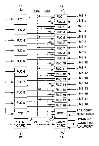
As is best seen in Figs. 1 and 2, the test access system 8 includes a number
of
line access cards 15, a test equipment card 35, a control card 25, and two
power
supplies 28, 29. Each of the line access cards 15, as can be seen in Fig. 2,
includes a
number of connectors for receiving corresponding connectors of a number of
communication lines, such as DS-3 transmission lines. The test equipment card
35
includes a number of connectors that receive corresponding connectors of a
number
of testing devices. The control card 25, which includes a programmable
processor
or CPU, coordinates the activities of the test access system 8, and may
further
2 0 communicate with a remote controlling unit via a communications card 18.
In accordance with a preferred embodiment of the present invention, and as
is depicted in Figs. 1 and 2, test access system 8 is designed to be modular
and rack
mountable. In accordance with this embodiment, test access system 8 includes
nine
line access cards 15, each of which comprises a front line card (FLC) 17 and a
rear
2 5 line card (RLC) 19. The test equipment card 35, according to this
embodiment,
comprises a front test card (FTC) 37 and a rear test card (RTC) 39. As is
further
seen in Fig. 3, the test access system 8 includes a double-sided motherboard
10, with
front circuit cards 12 plugging into the front of the motherboard 10 and rear
circuit
cards 14U, 14L plugging into the rear of the motherboard 10. Rather than a
single
3 0 full-height circuit card, two half-height circuit cards may be provided,
such as a top
rear card 14U and a bottom rear card 14L as is illustrated in Fig. 3.
CA 02376477 2001-12-06
WO 00/76224 7 PCT/US00/15632
In this configuration, nine front line cards 17 plug into the front of
motherboard 10.
The rear of the motherboard 10 provides coupling for a bank of nine top rear
line
cards 19 (i.e., RLC1 - RLC 17, odd numbers only) and a bank of nine bottom
rear
line cards 19 (RLC2 - RCL18, even numbers only), for a total of 18 line access
cards
15. Also coupled to motherboard 10 is a single test equipment card 35, with
the
front test card 37 and rear test card 39 of test equipment card 35 being
coupled to the
front and rear of motherboard 10, respectively. The control card (CC) 25,
communications card (COMC) 18, and each of the power supplies 28, 29 are also
connected to the motherboard 10.
In operation, four conventional BNC connectors (RXE, RXF, TXE, TXF)
provided on each line access card 15, and typically on rear line card 19 of
each line
access card 15, provide an interface connection for one bi-directional
communication line, such as a DS-3 transmission line. Similarly, the BNC
connectors (TXA, TXB, RXA, RXB) provided on the test equipment card 35, and
typically on the rear test card 39 of the test equipment card 35, provide a
dual test
port, which permits two pieces of communication line test equipment to be
connected thereto. The communication card 18 has an interface 20 which
includes
three connections that provide an RS-232 interface to and from the test access
system 8. However, it will be appreciated that any other type of communication
2 0 interface 20, such as a network interface 20, would work equally well.
In accordance with one embodiment of the present invention, the front line
card 17 of each line access card 15 provides control to a pair of rear line
cards 19. In
accordance with this embodiment, the front test card 37 of the test equipment
card
35 provides control to the rear test card 39. The front line cards 17 and the
front test
2 5 card 37 operate under control of the CPU provided in the control card 25.
The block diagram of Fig. 4 illustrates how the various cards are
interconnected through the motherboard 10, and the operation of the test
access
system 8 will best be understood by reference to that block diagram. A duplex
communication line is connected to each of the 18 rear line cards 19 (i.e.,
RLC1
3 0 through RLC18). Two pieces of communication line test equipment are
connected to
the rear test card 39 (RTC) and are selectively connected to one of the 18
RLCs 19.
CA 02376477 2001-12-06
WO 00/76224 8 PCT/US00/15632
This is achieved by means of two monitoring buses, MBl and MB2. The RTC 39 is
connected to both of the buses, MB 1 and MB2, and each RLC 19 is connected to
one of the two busses, MB1, MB2. In the embodiment illustrated in Fig. 4, the
odd
(upper) RLCs 19 are connected to MB1, and the even (lower) RLCs 19 are
connected MB2. The details of making such connections will be discussed
further
below. At this point it is sufficient to note that the connection between one
of the
monitoring buses, MB 1 or MB2, and an RLC 19 is made through one or more
relays.
In accordance with the embodiment shown in Fig. 4, each pair of RLCs 19
which occupy a common slot (i.e., one upper and one lower RLC 19) is
controlled
by a corresponding front line card 17. The front test card (F'TC) 37 of the
test
equipment card 35 controls the rear test card (RTC) 39. The FLCs 17 and FTC 37
are, in turn, controlled by the CPU provided in the control card (CC) 25. The
control
card 25 receives configuration commands from a controlling device, such as a
terminal or personal computer via an RS-232 link provided through the
communication card (COMC) 18. The communication card 18 can also provide
outgoing information through one of its communication ports 20, such as status
information provided by the control card 25. The use of the communication
links
makes it particularly efficient to perform remote testing.
2 0 An important aspect of a test access system 8 according to the present
invention involves ensuring signal integrity as the communication signal
pulses
propagate through the test access system 8. To ensure a high level of signal
transmission integrity, all signal paths within the test access system 8 are
designed to
exhibit the characteristics of an unbalanced transmission line with a 75 ohm
2 5 characteristic impedance, capable of transferring communication signal
pulses with
minimum attenuation, minimum distortion, and minimum crosstalk. However, it
will be appreciated that other impedance characteristics will work equally
well,
where appropriate.
In order to provide for such signal transmission integrity at the printed
circuit
3 0 board level, special layout techniques are employed. In accordance with
one
embodiment of the present invention, the cards of the test access system 8
which are
CA 02376477 2001-12-06
WO 00/76224 9 PCT/US00/15632
involved in transfernng information signals (e.g., the RLCs 19, the RTC 39,
and the
motherboard 10) are multilayered, impedance controlled printed circuit boards.
A
circuit board construction according to this embodiment is illustrated in Fig.
10,
which shows a section of a circuit board 50 with four layers, layer 1 through
layer 4.
However, it will be appreciated that a six or greater layer board could be
used.
All traces that transfer information signals are designed as unbalanced
transmission lines with a 75 ohm characteristic impedance. The transmission
lines
have a stripline configuration, consisting of a signal conductor and two
reference
planes, one above and one below the signal conductor. For maximum
electromagnetic induction (EMI) shielding, guard conductors are placed on
either
side of the signal conductors and surround every signal trace. The guard
conductors
are located on the signal layer of a printed circuit board and are connected
to both
reference planes at every half inch. Layers 1-3 depicted in Fig. 10 define the
stripline configuration, with the high frequency (I~) signal path provided at
layer 2
via conductor 52. The guard conductors 54, 54 are also provided in layer 2, on
either side of signal conductor 52. Layer 4 is used for the relatively low
speed logic
(control) signals. The substrate material of the printed circuit board is
preferably
FR-4.
The components used in the test access system 8 are also selected to have a
2 0 75 ohm characteristic impedance and excellent frequency characteristics.
Input and
output connections for information signal paths are provided by 75 ohm BNC
connectors mounted on the printed circuit board. Switching is provided by 75
ohm
HF relays with low insertion loss and crosstalk. The connections between the
rear
cards (RLCs, RTC) 19, 39 and the motherboard 10 are provided by 96 pin DIN
2 5 connectors. The DIN pin connector interface represents the only part of
the
information signal path in this embodiment in which impedance is not strictly
controlled.
However, signal integrity through these connectors is maintained by using a
pin assignment which simulates a co-axial transmission line, thus minimizing
the
3 0 discontinuity and making the connector effectively transparent to the
propagating
information signal. This pin assignment makes use of one pin from Column B
(i.e.,
CA 02376477 2001-12-06
WO 00/76224 10 PCT/US00/15632
middle column of pins) of the connector as a signal conductor and all eight
surrounding pins are used as shield conductors. A connector 60 incorporating
such a
pin configuration is illustrated in Fig. 11, wherein four separate pin
groupings are
shown. For example, the middle pin in row 31 is shown as connected to the
signal
conductor. At the same time, the remaining pins in rows 30-32 are connected
together and to the ground plane.
From the point of view of the electrical circuit design, all signal paths are
straight point-to-point electrical circuits with no taps. All junctions
between
different signal paths on the RLCs 19 and RTC 39 are made through relay
contacts.
On the RLCs 19, the "normal through" signal paths are tapped for monitoring
through 750 ohm bridging resistors, which virtually eliminate any effect of
the
tapping circuits on the communication lines in monitoring modes. As was
previously discussed, the RLCs 19 are connected to the monitoring busses, MB 1
and
MB2, through relays which are located on the motherboard 10 and controlled by
the
FLCs 17.
Figure 5 is a schematic block diagram useful in explaining how monitoring
bus switching is achieved in a test access system 8 of the present invention
so as to
ensure signal integrity. Figure 5 includes components which have already been
shown and discussed with respect to Fig. 4, and these components are
represented by
2 0 similar reference characters. Figure 5 illustrates, in particular, the
relays, which are
depicted as switches, which achieve monitoring bus switching. The RTC relays,
SWO, which are part of the RTC 39 in one embodiment, are capable of connecting
the RTC 39 to either MB 1 or MB2, depending upon the position of SWO. With
respect to the monitoring busses, MB 1 and MB2, each RLC 19 includes a
2 5 corresponding set of relays. By way of example, the upper (odd numbered)
RLCs 19
are coupled to associated relay sets SWl-SW17. In each instance, these relays
are
normally in their downward position (i.e., when not energized).
When no RLC relays are energized, end-to-end continuity of each monitoring
bus, MB 1, MB2, is provided and no RLCs 19 are connected to the monitoring
3 0 busses. The relays of the RLCs 19 are, however, activated one at a time,
so as to
place one of the RLCs 19 on the corresponding monitoring bus. When a set of
CA 02376477 2001-12-06
WO 00/76224 11 PCT/US00/15632
relays are so energized for a particular RLC 19, the relays are essentially
placed in
the upward position with respect to the depiction of Fig. 5, which breaks the
end-to-
end continuity of the corresponding monitoring bus and connects the
corresponding
RLC 19 to that monitoring bus. The described construction of the motherboard
10
guarantees that, at any time, there is only a single point-to-point connection
between
the RTC 39 and the selected RLC 19, and no other RLCs 19 are attached to the
monitoring bus. At the same time, that part of the monitoring bus which is not
in
use is disconnected and does not interfere with the propagation of the signal.
Figure 6 is a schematic block diagram of a rear line card (RLC) 19 in
accordance with an embodiment of the present invention. In general, RLC 19
includes two interfaces: one to the communication line and one to the
motherboard
10. The interface to the communication line is provided by four BNC
connectors.
The interface to the motherboard 10 is provided by a 96-pin DIN female
connector.
The RLC 19 shown in Fig. 6 includes one dual communication port with two
inputs (RXE and RXF) and two outputs (TXE and TXF). RLC 19 also includes a
plurality of relays, which are represented as switches in Fig. 6, which are
operated
under control of the corresponding FLC 17. There are two "normal-through"
paths,
namely, from RXE to TXF and from RXF to TXE. RLC 19 also provides four paths
to a monitoring bus. Two of the paths, from a MON_TXE to TXE and from
2 0 MON TXF to TXF, are direct paths. The other two paths are from RXE to
MON_RXE and from RXF to MON_RXF and can be direct paths or paths through
the B or B&T circuits, depending upon the desired test mode.
Each RLC 19 has the capability of providing loopback connections at the
communication port, from RXE to TXE and from RXF to TXF. It should be noted
2 5 that, in a preferred embodiment, two rear line cards 19 (upper and lower)
are used in
each slot. This arrangement has the advantage that, in the event that a line
card
needs to be replaced, only one line needs to be placed temporarily out of
service. It
will be appreciated that a single line card accommodating two duplex
communication lines may also be employed.
3 0 The rear test card (RTC) 39 is preferably provided in two types. Figures
7A
and 7B are schematic block diagrams of a Type 1 RTC and a Type 2 RTC,
CA 02376477 2001-12-06
WO 00/76224 12 PCT/US00/15632
respectively. Both RTC types includes one dual test port with two inputs (RXA
and
RXB) and two outputs (TXA and TXB). Each RTC 39 also includes a plurality of
relays, depicted as switches, which are operated under control of a front test
card
(FTC) 37. The Type 1 RTC 39, shown in Fig. 7A, can provide loopback for many
of
the inputs to any of the outputs. The Type 2 RTC 39, shown in Fig. 7B, can
provide
loopback from RXA to TXA and from RXB to TXB only. On the other hand, RTC
Type 1 cannot provide loopback at the unused port when A Split, AX Split, B
Split
and BX Split modes are selected.
Four connectors labeled NR in Figs. 7A and 7B provide connection to the
next rack mount in "daisy-chain" configurations. Depending on the position of
the
"daisy-chain" contacts shown in Figs. 7A & 7B, the test port can be connected
either
to one of the monitoring buses of the present rack mount or the next rack
mount.
The "crossover' contacts provide direct or cross-connections for the inputs
(RXA,
RXB) and for the outputs (TXA, TXB). The "loopback" contacts provide loopback
connections from RXA to TXA and from RXB to TXB. The "MON Bus Select"
contacts provide connections to either of the two monitoring buses, MBI, MB2.
RTC 39 includes three interfaces: one to the communication line test
equipment; one to the next rack mount; and one to the motherboard 10. The
interface to the communication line test equipment is provided by four BNC
2 0 connectors, such as RXA, TXA, RXB and TXB shown in Fig. 2. The interface
to
the next rack mount is provided by four BNC connectors labeled "next rack,"
which
is also shown in Fig. 2. The interface to the motherboard 10 is provided by
one 96
pin DIN female connector.
Figure 8 is a functional block diagram illustrating the operation of a front
2 5 line card (FLC) 17 in accordance with an embodiment of the present
invention. For
purposes of illustration, and not of limitation, an FLC 17 is shown coupled to
a pair
of rear line cards 19, RLC 1 and RLC2, each of which is controlled by FLC 17.
FLC
17, in turn, is controlled by a CPU provided in control card 25. FLC 17
includes two
control blocks (CTRL1 and CTRL2), each of which provides control to a
respective
3 0 RLC 19 (RLC 1 and RCL2, respectively).
FLC 17 further includes a set of relays for defining part of a respective
CA 02376477 2001-12-06
WO 00/76224 13 PCT/US00/15632
monitoring bus MB1, MB2. Two light emitting diodes (LED1 and LED2) provided
on the front of FLC 17 indicate the status of the corresponding RLCs 19. By
way of
example, when a respective RLC 19 is in a test mode, the corresponding LED is
illuminated, whereas when a loopback mode is selected, the corresponding LED
blinks. In addition to relay drivers, control blocks CTRL1 and CTRL2 also
includes
two 8-bit control registers. Registers 1 and 2 are provided in CTRLI for RCL1,
and
Registers 3 and 4 are provided in CTRL2 for RLC2.
The bits in the odd register (Register 1 and Register 3) have the following
effect on the relays of the corresponding RLC 19 in accordance with an
embodiment
of the present invention:
D7: when 0, closes "normal through" path from RXE to TXF.
when 1, connects RXE to monitoring bus.
D6: when 0, closes "normal through" path from RXE to TXF.
when 1, connects TXF to monitoring bus.
D5: when 0, selects B & T circuit.
when 1, selects direct connection from RXE to monitoring bus.
D4: when 0, selects split mode.
when 1, selects monitoring mode.
D3: when 0, closes "normal through" path from RXF to TXE.
2 5 when 1, connects RXF to monitoring bus.
D2: when 0, select B & T circuit.
when 1, selects direct connection from RXF to monitoring bus.
3 0 D1: when 0, selects split mode.
when 1, selects monitoring mode.
CA 02376477 2001-12-06
WO 00/76224 14 PCT/US00/15632
D0: when 0, closes "normal through" path from RXF to TXE.
when 1, connects TXE to monitoring bus.
Similarly, the even control register (Registers 2 and 4) have eight bits which
have the following effect on the relays of the corresponding RLC 19 in
accordance
with an embodiment of the present invention:
D7: when 0, disconnects MON_RXE and MON TXF from the RLC.
when 1, connects MON_RXE and MON TXF to the RLC.
D6: when 0, disconnects MON_RXF and MON_TXE from the RLC.
when 1, connects MON_RXF and MON_TXE from the RLC.
D5: when 0, de-selects loopback from RXE to TXE.
when 1, selects loopback from RXE to TXE.
D4: when 0, selects loopback from RXF to RXF.
when 1, de-selects loopback from RXF to TXF.
D3: when 0, disconnects the shield of RXE-TXF switching circuit to the
shield of the monitoring bus.
when 1, connects the shield of RXE-TXF switching circuit to the
shield of the monitoring bus.
D2: when 0, disconnects the shield of RXF-TXE switching circuit to the
shield of the monitoring bus.
when 1, connects the shield of RXF-TXE switching circuit to the
shield of the monitoring bus.
D1: when 0, disconnects the shield of RXE-TXF switching circuit to the
CA 02376477 2001-12-06
WO 00/76224 15 PCT/US00/15632
shield of the RXF-TXE switching circuit.
when l, connects the shield of RXE-TXF switching circuit to the
shield of the RXF-TXE switching circuit.
D0: when 0, turns off the LED for the corresponding RLC.
when l, illuminates the LED for the corresponding RLC.
It will be appreciated that the control registers CNRL1 and CNRL2 of RLC
19 allow a large number of different modes of operation by virtue of the
different 8
bit words that can be provided in each register. Table 1 provided below
exemplifies
a number of different modes of operation that may be available for each RLC
19.
The described modes correspond to various test modes defined by the Bellcore
standards for testing communication equipment.
CA 02376477 2001-12-06
WO 00/76224 PCT/US00/15632
16
TABLE 1
Coi!rol Con;:ef
R.~.;.n R.j.;.;
1 2I;)
(~) (i2,
(R1, fi4)
R~) ~
f~, D D 0 D D D D D D D ~ D D D D 0
7 G 6 .i s 2 1 0 7 0 i 3 2 1 0
6 b .:
EOU T.tont;x X 0 0 0 X 0 0 0 1 0 I 0 1 0 O 1
0
FpQ 1"4ont;or'X 0 0 O X O 0 0 0 1 ~ 0 0 1 I 1
I I 0 I 0
EF(~Q ~nl;or X 0 0 0 X 0 O 0 1 S ( 0 1 1 0 1
I 0
ECU SpL; (r X 1 0 O X 0 O t 1 1 ~ O 1
Loop) _ (I) O (1)
~
El)Q Spla w X 1 1 0 X 0 O 1 1 1 0 0 1 1 1 1
6&: (= Loop) (f) . I1)
FOU SFB: (~ X 0 0 1 X 1 0 0 1 1 0' 0 1 1 5 1
Locp) . II)~ (11
._ :
FDO Spf : w X 0 0 1 X 1 1 0 1 1 0 0 1 1 't-.
B.~T I= Loop) (1) I (I) . .
Erpn Spsi; X 1 0 1 X 1 O 1 1 1 0 0 1 S 1 1
.
EFpO Spat w X 1 1 1 X 5 1 1 1 1 0 0 1 1 1 1
BLT
AppS,fK X 1~ 0 1 X 0 0 0 1 00 0 1 0 0 1
w EST X 1 1 1 X 0 O 0 1 0 ( 0 1 0 O t
A pp Split . 0 .
EDU Spit X 0 0 0 X 1 O 1 0 1 ~0 0 0 1 0 1
B00 Split w X 0 0 0 X 1 1 1 0 1 0 0 0 1 O S
Sd~T - .
A6CX) Split X 1 0 1 X 1 0 1 1 1 0 0 1 1 1 1
~
r
/~ B W Spl1 X 1 1 1 X 1 1 1 1 1 0 0 1 1 1 1
t w BST
E Loop - . X 0 0 0 X 0 0 1 0 0 1 0 O 0 1 6l
.
F Loop X 0 0 1 X 0 O 0 0 0 0 S 0 0 1 6=
EF Loop X 0 0 1 X 0 0 1 0 0 1 5 0 0 1 6:
D51 Drop b~ X 1 1 1 X 0 0 0 1 I 0 0 1 1 l
In.art A' .
D51 Drop L. X 0 0 0 X 1 1 1 1 1 0 O 1 1 I 1
In.art 6'
CA 02376477 2001-12-06
WO 00/76224 17 PCT/US00/15632
Figure 9 is a schematic block diagram illustrating the operation of a front
test
card (FTC) 37 in accordance with an embodiment of the present invention. FTC
37
controls the relays in the rear test card (RTC) 39 and is itself controlled by
the CPU
provided in the control card 25. FTC 37 includes a single control block
(CTRLI)
which provides control to the RTC 39. One light emitting diode (LED) on the
front
of FTC 37 indicates the status of the RTC 39. When RTC 39 is in a test mode,
the
LED is illuminated, whereas when RTC 39 is in a loopback mode, the LED blinks.
FTC 37 contains relay drivers for RTC 39 and two 8-bit control registers.
The bits of control Register 1 of CTRL1 in FTC 37 have the following effect
on the relays of RTC 39 in accordance with an embodiment of the present
invention:
D7: when 0, selects MON RXB line from the upper monitoring bus
(MB 1 ).
when 1, selects MON_RXB line from the lower monitoring bus (MB2).
D6: when 0, de-selects loopback between RXB-TXB (if crossover is not
active).
when 1, selects loopback between RXB-TXB (if crossover is not active).
2 0 D5: not used.
D4: not used.
D3: when 0, selects MON TXA line from the upper monitoring bus
2 5 (MB l ).
when 1, selects MON_TXA line from the lower monitoring bus (MB2).
D2: when 0, selects MON_TXB line from the upper monitoring bus
(MB 1 ).
3 0 when 1, selects MON TXB line from the lower monitoring bus (MB2).
CA 02376477 2001-12-06
WO 00/76224 18 PCT/US00/15632
Dl: when 0, de-selects loopback between RXA-TXA (if crossover is not
active).
when 1, selects loopback between RXA-TXA (if crossover is not active).
D0: when 0, selects direct connections to TXA and TXB (crossover).
when 1, selects cross-connections to TXA and TXB (crossover).
The bits of control Register 2 of CNRL1 in FTC 37 have the following effect
on the relays of the RTC 39 in accordance with an embodiment of the present
invention:
D7: not used.
D6: not used.
D5: when 0. selects MON RXA line from the upper monitoring bus
(MB 1 ).
when 1, selects MON RXA line from the lower monitoring bus (MB2).
2 0 D4: when 0, selects direct connections to RXA and RXB (crossover).
when 1, selects cross-connections to RXA and RXB (crossover).
D3: not used.
2 5 D2: when 0, selects local Rack.
when 1, selects Next Rack.
D 1: not used.
3 0 D0: when 0, turns off the test LED.
when l, illuminates the test LED.
CA 02376477 2001-12-06
WO 00/76224 19 PCT/US00/15632
It will therefore be appreciated that the different combinations of bits
available in the two control Registers of CNRL1 in FTC 37 will produce a large
number of operating modes in RTC 39. Table 2 provided below exemplifies
various
operating modes available for RTC 39 in accordance with an embodiment of the
present invention.
CA 02376477 2001-12-06
WO 00/76224 2~ PCT/US00/15632
TABLE 2
Ccn;rctFrjrcn Goritrc:
1 Fsej
(.s l l , r;~:2
lR2)
!.'.oCe D D 0 D D D D D D D D 0 D D D p
7 I 6 4 I I I I 7 C 6 S 3 2 1 I
E 7 2 1 0 p
E f.S,:ni;or f3 II)x ~ ~ A 0 ~ X X ~ 0 ~ 0 ~ 1
Loop) A X 0 ' I. ' X X '
EX l.Sor:;or f~ ' X X ~ /, 0 1 ~ X A O X 0 X t
Loap) /1 0 A X (1l
(1l
F Lbry;oc (r1 0 X X A A o o X X A 0 X 0 X ~
loop) ! /1 Itl t
FX LS~r~;or (a O X X A ( 0 t X X h 0 X 0 X ~
Loop) ' ~ A A (11 (I) 1
EF AtNitor A O X X ( A 0 0 X X Jl 0 X 0 X t
.e,
EFX Li~nttot A O X X A A 0 1 X X A 0 X 0 X 1
E Sfi:; f3 lacp) O X X A A 0 0 X X A O X 0 X ~
A I1) 1
EX Spli t V. Loc,O X X I1A 0 1 X X A 1 X .O X 1
) A (1) ~
F sr~~a N Loop) O X X A A o 0 X X f. O X o X t
.e: ( ( ~ ~ ~ ~
It)
FX SpFt (S Lo-op)O X X A A 0 1 X X A 1 X O X t
A ~ I1)
EF Sfli; ~ A O X X A /1 0 o X X A o X o. X t
I ' ~
EFX spc: Il 0~,X X A A 0 1 X X /l t X O X 1
ASpzt ' A O X X A A 0 0 X X A t X O X 1
AXSp'at A O X X A A 0 1 X X A O X O X t
B Sp:; l1 0 X X l1A 0 0 X X A 1 X O X 1
l3X S~a; A O X X A A 0 1 X ~X f. 0 X O X t
ABSp:: A 0 X X A A 0 0 X X A 1 X O X.t
AEC S~t ' A 0 X X A A 0 1 X X A O 'X O X S
I '
~ Lo.oQ x o x x x x ' o x x x o x o x
t
a Log X t X X X X p o X x X o X o X eL
~ .
~a Logy x t x x x x t o x x x o x o x al.
Prir,ary Loap' O X X X X 1 0 X X X 0 X O X EL
X ~ (
Secondary Loop' 1 X X X 0 0 X X X 1 X O X EC
( X
D51 Orop 3 IneertO X X A /~ 0 1 X X A 1 X O X 1
A' /~ I I I I I
D51 Drc~ 4 Inrea 0 X X A A 0 0 X X A 0 ~ O X 1
B' A I I [ ~
Noxt Ra:k ~ X' X X X X X X X X X X X X ~. X 1
CA 02376477 2001-12-06
WO 00/76224 21 PCT/US00/15632
In accordance with another embodiment, and with reference to Figures 12A
and 12B, a test access system 101 in accordance with the principles of the
present
invention provides a manual patching capability through employment of line
access
cards 115 which include single or multiple patch circuitry. A test access
system 101
according to this embodiment of the present invention combines the features
and
advantages of the automatic remote controlled test access capabilities
described
hereinabove with the convenience and flexibility of manually establishing
desired or
needed cross-connections.
A test access system employing a cross-connect capability provides a
termination point for permanently connected equipment, and, through use of
patch
circuitry according to this embodiment, also accommodates a number of
switching
jacks, typically coaxial jacks, whereby patch cords may be employed to
temporarily
redirect connections. The signal pathways of the patching circuitry, including
those
established through switching jacks and patch cords/plugs, are preferably
implemented to have a characteristic impedance, such as a 75 ohm
characteristic
impedance, and excellent frequency characteristics.
By having equipment and facilities terminate on a test access system
employing a cross-connect capability, a service provider is able to manually
patch
around trouble spots, or rearrange equipment and facilities without service
2 0 interruption. A service provider may also test selected communication
lines
established through either hardwired connections or temporary patch
connections.
As is shown in Figures 12A and 12B, test access system 101 includes a
chassis 109 which defines the physical space needed to house the various cards
of
the system 101. Chassis 109 includes an control bus 113 which provides for the
2 5 communication of control and information signals between each of the line
access
cards 115 and other cards and busses of the test access system 101. Power
distribution to all of the cards of system 101 is also provided by chassis
109.
Chassis 109 further provides physical connections to all control connections
of
system 101. Central processing unit (CPU) 107 coordinates the various control
3 0 functions with respect to the cards of test access system 101. CPU 107
also controls
the various communications tasks with respect to the management software and
CA 02376477 2001-12-06
WO 00/76224 22 PCT/US00/15632
other linked test access systems 101.
Each of the line access cards 115, according to this embodiment of the
present invention, provides jack interface access to one or more corresponding
communication lines, such as DS-3 transmission lines. A line access card 115
employing a jack interface access capability also provides for the
establishment of
cross-connections via dedicated busses. Line access cards 115 further provide
for
test access to high speed communication lines via a test bus 116 (e.g.,
network of
relays), and access to one or more test busses for accessing one or more
testing
devices. A test card 111 provides an interface between line access cards 115,
selected communications lines to be tested, and external or built-in test
equipment.
A power supply 105 provides the required power for the test access system 101.
An embodiment of a line access card 115 having a patch access capability is
shown in Figure 13. Line access card 115, in accordance with this embodiment,
provides for cross-connections, switching, testing, and monitoring, including
establishing permanent and temporary connections and terminations,
respectively, to
occur at a facility side 100 of a telecommunications network via transmit and
receive
lines, TXF 110 and RXF 120, respectively. Figure 14 provides a front view of
line
access card 115 embodied in a module designed for "plug and play" operation
when
installed in a test access system. For example, modular line access card 115
shown
2 0 in Figures 13 and 14 may be slid into an available slot of chassis 109
shown in
Figures 12A and 12B. When properly installed, signal and power connectors
respectively provided on chassis 109 and line access card 115 matingly engage,
without need of manual intervention, to establish required signal and power
connections therebetween.
2 5 The embodiment of line access card 115 shown in Figures 13 and 14
incorporates a single patching capability. As can be seen in Figures 13 and
14, line
access card 115 includes jacks 144 to provide a user with manual and direct
access
to two communication lines or channels routed through line access card 115.
Each
of the facility jacks 144, which are shown vertically aligned as MON
(monitor),
3 0 OLTT (output) and IN (input), respectively, correspond to a particular one
of the two
communication lines (channels).
CA 02376477 2001-12-06
WO 00/76224 23 PCT/US00/15632
As is further illustrated in Figures 13 and 14, line access card 115, which
incorporates a single patch circuit 140, is designed to operate within a test
access
system by providing a patch connection 140 which permits direct access to the
facility side 100 of the communication line circuit. The patch circuit 140
includes
three interfaces, namely, facility interface 130, switching circuit interface
136, and
jack interface 144. The facility interface 130 is connected to equipment of
the
facility side 100 (RXF, TXF) of the network. The switching circuit interface
136 is
internally connected to the switching circuit 150 of the line access card 115.
The
jack interface 144 includes three jack connectors located on the front of the
line
access card 115 labeled IN, OUT, and MON, respectively.
The IN jack provides access to the equipment to which the IN jack is
terminated, and can be used to access or transmit signals into the equipment
input.
The OUT jack is used to monitor the output signals from the equipment to which
the
OUT jack is terminated. The MON jack serves a similar function as the OUT jack
by monitoring communication signals, but without breaking the communication
line
circuit. In this manner, the MON jack allows for in-service bridging of a
digital line
without interfering with line operation. In a preferred embodiment, the OUT
jack
observes the output signals from equipment to which it is terminated by
insertion of
a patch cord into the OUT jack circuit.
2 0 As is also illustrated in Figure 14, line access card 115, which includes
a
single patch circuit 140, further includes two LED's 148, 152 located on the
front
panel of line access card 115. The first LED is a bicolor LED 148 which
represents
a "TEST/ALM" LED. LED 148 corresponds to a line access port. In a "test" mode,
the TEST/ALM LED 148 illuminates a particular color (e.g., green) to indicate
2 5 whether a certain communication line port is being tested or not. In
"alarm" mode,
the TEST/ALM LED 148 illuminates a second color (e.g., amber) to indicate an
alarm condition on a certain communication line port.
The second LED is a red LED 152 which represents a "TRACER" LED.
The TRACER LED 152 is used for identification of the cross-connections between
3 0 different communication line circuits. The TRACER LED 152 illuminates when
a
patch cord is inserted into its corresponding MON jack or when activated by a
CA 02376477 2001-12-06
WO 00/76224 24 PCT/US00/15632
corresponding switch, such as a toggle or plunger switch; the other
communication
line circuit that cross-connects with the initial circuit also illuminates its
corresponding tracer LED 152. This is accomplished by connecting the tracer
pins
on the rear of the test access unit with the tracer pins of other test access
units via
wire wrap or Telco pin connectors.
In an alternative embodiment, as is shown in Figures 15-17, a line access
card 115 may incorporate a dual patch capability by employment of a patch
circuit
140 associated with the facility side 100 of a telecommunications network and,
in
addition, a patch connection 180 connected to equipment side 200 of the
network.
In accordance with this embodiment, line access card 115 incorporates dual
patch
circuits 140 and 180 to facilitate line testing at a remote location (i.e.,
customer
premises of the communication lines incoming from an equipment location). The
group of line access cards 115 shown in Figure 12B, for example, depict line
access
cards incorporating a dual patch capability.
As previously stated, each patch circuit 140, 180 includes an equipment
interface 130, 131, a switching circuit interface 141, 181, and a jack
interface 144,
184, respectively. The equipment interface 130, 131 of each patch circuit 140,
180
is connected to the facility side 100 or equipment side 200 of a communication
line
circuit. The switching circuit interface 141, 181 of each patch circuit 140,
180 is
2 0 internally connected to the switching circuit 150 of the line access card
115. The
jack interface 144, 184 of each patch circuit 140, 180 includes three jack
connectors
located on the front of the line access card 115.
The three jack connectors are labeled IN, OUT, and MON, respectively, and
are associated with either the equipment or facility sides 200, 100. Each IN
jack
2 5 provides access to the equipment to which it is terminated, and can be
used to
transmit signals into the equipment (or facility) input. The OUT jack is used
to
monitor the output signals from the equipment to which it is terminated. The
MON
jack, as previously mentioned, provides for in-service bridging of a digital
line
without interfering with its operation.
3 0 Temporary connections may be made using patch cords between jack
circuits, thereby permitting restoration of failed services or providing
temporary
CA 02376477 2001-12-06
WO 00/76224 25 PCT/US00/15632
connections for cut-overs. The normal function of a patch cord when used
within a
cross-connect system environment is to temporarily re-direct a circuit
connection to
a termination point different from that established by the circuit's hardwired
connection. For example, when a plug of a patch cord is inserted into either
the
OUT jack or IN jack of a line access card 115, the circuit connection to the
hardwired connection is broken, such that a new conductivity path is
established
over the patch cord. The patch plug connected at the opposing end of the patch
cord
may then be inserted into an appropriate OUT or IN jack of another line access
card
provided in the same or different chassis to establish a new and generally
temporary
cross-connection through the patch cord.
It is understood in the industry that TRACE wire or lamp wire is used in a
cross-connect system to connect the TRACE LED's of each of the cross-connected
circuits for purposes of manually tracing a connection. In accordance with a
further
embodiment of the present invention, TRACE wire and patch cord connections may
be utilized to effectively form scanning busses over which scanning signals
may be
transmitted in accordance with a unique scanning methodology. This
unconventional use of TRACE wire and patch cord connections within a test
access/cross-connect system environment, in combination with an unique
scanning
protocol, provides for the continuous and near real-time acquisition of
connection
2 0 status information which may be maintained and updated in a centralized
cross-
connect database.
It is readily appreciated by those skilled in the art that maintaining
accurate
connection records for hundreds of thousands of connections has proven to be
impractical, if not impossible, using conventional manual tracing approaches.
A
2 5 cross-connect monitoring system according to this embodiment of the
present
invention provides for accurate and continuous electronic monitoring and
updating
of connection records for any number of connections. Details for implementing
this
embodiment of an intelligent digital test access/cross-connect system that
electronically and automatically identifies and monitors all connections
established
3 0 through the line access cards of the system on a continuous basis may be
found in
co-owned U.S. Serial No. 08/972,159, filed November 17, 1997 and entitled
CA 02376477 2001-12-06
WO 00/76224 26 PCT/US00/15632
"System and Method for Electronically Identifying Connections of a Cross-
Connect
System," which is hereby incorporated herein by reference in its entirety.
Figure 15 shows a layout of a line access card 115 provided with a dual patch
circuit capability. Line access card 115 shown in Figure 15 includes a number
of
interfaces in accordance with an embodiment of the present invention. A 48-
finger
DIN connector 117 provides an interface to the control bus 113 and
testlmonitor bus
116 shown in Figure 12A. This interface 117 includes data bus, control
signals, and
power supply lines. Interface 119 includes four communication line port
connections, which in this embodiment constitute four BNC connectors. Two
patch
circuits 140, 180 and corresponding patch connector sets 144, 184 provide
manual
access to the facility and equipment sides 100, 200 of the communication line
circuits.
With further reference to Figures 16 and 17, a line access card provided with
a dual patching capability includes two groups of LED's 148, 152 located on
the
front panel of the line access card 115. The first group consists of bicolor
LED's
148 labeled "TEST/ALM". Each of the LED's 148 corresponds to a line access
port. In a "test" mode, the TEST/ALM LED's 148 illuminate a particular color
(e.g.,
green) to indicate whether a certain communication line port is being tested
or not.
In an "alarm" mode, the TEST/ALM LED's 148 illuminate a second color (e.g.,
2 0 amber) to indicate an alarm condition on a certain communication line
port.
The second group consists of two red LED's 152 labeled "TRACER," and
used for identification of cross-connections established between different
communication line circuits. The TRACER LED's 152 illuminate when a patch
cord is inserted the corresponding MON jack or when activated by a
corresponding
2 5 switch, such as a toggle or plunger switch; all other communication line
circuits that
cross-connect with the initial communication line circuit also illuminate
their
corresponding TRACER LED's. This is accomplished by connecting the tracer pins
on the rear of a test access unit with the tracer pins of other test access
units via wire
wrap or Telco pin connectors.
3 0 In addition to a line access card 115 of the present invention including
either
single or dual patch connection capabilities, a line access card 115 may also
include
CA 02376477 2001-12-06
WO 00/76224 27 PCT/US00/15632
a performance monitoring feature 90, as is shown in Figures 18 and 19, which
is
capable of monitoring communication line circuits for variety of line
anomalies and
error information. Refernng now to Figures 18 and 19, each line access card
115 is
equipped with a monitoring function for collecting line failures from both the
facility
and equipment sides 100, 200 of a number of different communication lines. The
monitoring function in accordance with this embodiment of the present
invention
may be implement in a test access system employing no patch, single patch, and
dual
patch circuitry.
Preferably, a performance monitoring function circuit 90 incorporated in a
line access card 115 of the present invention represents a high impedance
device,
such that information signals passing through the line access card 115 are not
degraded. This feature is important to allow nonintrusive monitoring of the
communication line. In one embodiment, line information is constantly
collected
and stored in 15 minutes registers, 1 hour registers, and one day registers.
Performance monitoring occurs on each of the line access ports 91, 93
simultaneously; that is, no multiplexing occurs in the preferred embodiment,
which
allows the performance monitor feature to accept simultaneous real time data
from
each of the associated lines (e.g., RXE, RXF). The information is stored in
the
registers and can be retrieved at any time by the management system 12.
2 0 Once an alarm condition is detected, the CPU immediately sends an alarm
condition signal to the management system, which, upon reception, presents it
to the
user. Each alarm event is presented to the management software via the CPU
with a
time of day and date stamp. Register information may be collected from the CPU
at
any time. If SNMP management software with paging capability is used, the
2 5 management software can page the user for each alarm occurrence. A remote
management system well suited for use in a test access system environment of
the
present invention is disclosed in co-owned U.S. Serial No. 09/219,810, filed
December 23, 1998 and entitled "Test Access and Performance Monitoring System
and Method for Cross-Connect Communication Networks," which is hereby
3 0 incorporated herein by reference in its entirety.
Performance parameters supported by the performance monitoring and alarm
CA 02376477 2001-12-06
WO 00/76224 28 PCT/US00/15632
functions of a test access system of the present invention include near-end
line
performance parameters, and near-end path performance parameters and alarms.
Performance monitoring and alarm features are intended to monitor and detect
both
line and path anomalies and defects. Line anomalies include a bipolar
violation
(BPV), which occurs as a non-zero pulse of the same polarity of the previous
pulse,
and excessive zeros (EXZ), which includes any zero string length greater than
7
contiguous zeroes (BBZS), as well as any zero string length greater than 15
contiguous zeroes (AMI).
Path anomalies include CRC-6 errors and frame bit errors (FE). CRC-6
errors are detected when a received CRC-6 code does not match the CRC-6 code
calculated from the received data. Frame bit errors are bit errors occurnng in
the
received frame bit pattern. Line defects include loss of signal (LOS), while
path
defects comprise out-of-frame (00F), severely errored frame (SEF), and alarm
indication signals (AIS). Severely errored frames include the occurrence of
two or
more frame bit errors within a window. An AIS event indicates the occurrence
of an
unframed signal having a "one's density" of at least 99.9% present for at
least three
seconds. This is indicative of an upstream transmission interruption.
For near-end line failures, an LOS occurs when the LOS defect persists for
2.5 seconds, ~ .5 second. Near-end path failures include and AIS and LOS,
while
2 0 far-end path failures include a remote alarm indication (RAI), which
indicates a
signal transmitted in the outgoing direction when equipment determines that it
has
lost the incoming signal. Other indicators include the near-end path failure
count
(count of near-end path failures) and far-end path failure count. Near-end
line
performance parameters include code violation-line (CV-L), errored second line
2 5 (ES-L), and severely errored second-line (SES-I). Near-end path
performance
parameters include code violation-path (CV-P), errored second path (ES-P),
severely
errored second-path (SES-P), SEF/AIS second path (SAS-P), and unavailable
second path (UAS-P). Alarms supported include red alarm, blue alarm, yellow
alarm, corresponding to loss of signal (LOS), alarm indication signal (AIS)
and
3 0 remote alarm indication (RAI), respectively.
Figures 20-22 illustrate various connection configurations for facilitating
CA 02376477 2001-12-06
WO 00/76224 29 PCT/US00/15632
non-intrusive monitoring of a number of telecommunication lines 202 using a
remote test access system 201 of the present invention. The manner of
connecting
selected communication lines 202 between the remote test access system 201 and
one or more testing devices 203 varies depending on a number of factors,
including
data rate, sensitivity of the particular testing device 203, and the distance
between
the test access system 201 and testing device 203.
With reference to Figure 20, there is shown a remote test access system 201
through
which a number of communication lines 202 pass using either or both of
hardwired
or patch connections as described above. Selected communication lines 201 may
be
connected to testing device 203 and subjected to non-intrusive monitoring and
testing by testing device 203. In the embodiment of Figure 20, bridging
resistors
205 are coupled between selected communication lines 202 passing through test
access system 201 and testing device 203. The value of the bridging resistors
205 is
typically nine to ten times greater than the characteristic impedance of the
communication line subject to testing.
The value of bridging resistors 205 should be sufficiently large to prevent
the
testing device 203 from interfering with the normal data flow on the
communication
line 202. It will be appreciated that in this configuration, bridging
resistors 205 in
conjunction with the input impendence of testing device 203, which is
typically
2 0 equivalent to the characteristic impedance of the communication line 202
subject to
testing, will result in appreciable signal attenuation (e.g., -20 dB) at the
point of
monitoring. It is noted that certain testing devices 203 may not be capable of
recovering highly attenuated signals for purposes of communication line
testing.
Concerning the testing configuration shown in Figure 21, the connection
2 5 arrangement between test access system 201 and testing device 203 provides
for 0
dB signal attenuation at the monitoring point. In this configuration, testing
device
203 is required to provide a sufficiently high input impedance so as to avoid
disrupting the normal flow of data on the communication line 202 subject to
testing.
In general, the connection between test access system 201 and testing device
203
3 0 should be very short. The testing configuration shown in Figure 21 is best
suited for
relatively low data rates, such as DS-1 data rates, since a substantial degree
of
CA 02376477 2001-12-06
WO 00/76224 30 PCT/US00/15632
interference with normal data flow on the subject communication line 202 may
result at relatively high data rates.
The testing configuration depicted in Figure 22 provides for 0 dB signal
attenuation at the monitoring point and minimal interference with the normal
flow of
data on the communication line 202 subject to testing. The testing
configuration of
Figure 22 is particularly well-suited for monitoring of high data rate
transmission
lines 202 using testing devices 203 that may require, or prefer, line level
signals for
performing monitoring and/or testing functions. In accordance with the
embodiment
shown in Figure 22, bridging resistors 205 are coupled between selected
communication lines 202 passing through test access system 201 and testing
device
203. As in the embodiment shown in Figure 20, the value of bridging resistors
205
is sufficiently high so as not to cause interference with the normal flow of
data on
the communication line subject to testing, which results in appreciable signal
attenuation at the monitoring point.
An amplifier 207 is coupled between each of the bridging resistors 205 and
the corresponding input of testing device 203. Amplifiers 207 preferably
increase
the gain of the signal subject to testing to a level equivalent to offset the
attenuation
resulting from inclusion of bridging resistors 205 in the test signal path.
Amplifiers
207 may include circuit elements that condition the signals subject to testing
in a
2 0 manner most appropriate for a given testing device 203. For example,
amplifiers
207 may include filtering elements to minimize any phase distortion that may
result
from amplification of the signals attenuated by bridging resistors 205.
Although a preferred system and method embodying the present invention
have been disclosed for illustrative purposes, those skilled in the art will
appreciate
2 5 that many additions, modifications and substitutions are possible without
departing
from the scope of the present invention. For example, a system has been
described
for providing testing access to DS-3 communication links. It is contemplated
that
the present invention may be utilized for other transmission rates and
protocols,
including the European E-3 protocol (34 Mbps) or STM-1 protocol (155 Mbps). It
3 0 is further contemplated that the present invention may be utilized for
substantially
higher frequency signals, such as DS-5 signals which, in Europe, provide a
capacity
CA 02376477 2001-12-06
WO 00/76224 31 PCT/US00/15632
of 565.148 Mbps, as well signal rates on the order of 1 or more billion bits
per
second (Bbps). All such variations are intended to be within the scope of the
invention as provided in the appended claims.