Note: Descriptions are shown in the official language in which they were submitted.
CA 02376915 2001-12-12
WO 00/77950 PCT/US00/16269
1
ADJUSTING MAXIMUM TRANSMIT POWER TO MAINTAIN
CONSTANT MARGIN FOR ADJACENT CHANNEL POWER
REJECTION
BACKGROUND OF THE INVENTION
1. Field of the Invention
The present invention generally relates to wireless telephones. More
specifically, the present invention relates to techniques involving the
automatic adjustment of RF amplification circuitry.
II. Description of the Related Art
Signals transmitted by wireless telephones are required to satisfy various
requirements. For instance, Code Division Multiple Access (CDMA) cellular
phones are mandated by the FCC to limit out of channel distortion when
transmitting in the radio frequency (RF) spectrum. Adjacent Channel Power
Rejection (ACPR) is a metric frequently used to measure out of channel
distortion. ACPR is represented as a curve across the spectrum that is
centered
at a transmitted RF signal's center frequency. At this center frequency, an
ACPR
curve is at its maximum. However, an ACPR curve symmetrically attenuates
as frequencies depart from this center frequency. ACPR curves are compared
against the spectral power characteristics of transmitted RF signals. Current
CDMA standards, such as IS-98, require the spectral power characteristics of
transmitted CDMA signals to be below a defined maximum ACPR curve at all
frequencies and transmit power levels. When a signal complies with such a
requirement, the signal is said to have passing margin. When a signal fails to
comply with such a requirement, its out of channel distortion is excessive.
A wireless phone contains components that amplify RF signals so that
they have sufficient power for transmission. Before amplification, a properly
CA 02376915 2001-12-12
WO 00/77950 PCT/US00/16269
2
modulated RF signal has negligible out of channel distortion. An amplified
signal's out of channel distortion will also be negligible if the
amplification
process is linear. However, if a signal has been amplified by a non-linear
amplification process, its spectrum will include increased out of channel
distortion. This increased out of channel distortion may cause a wireless
phone
to exceed the maximum allowed ACPR.
Electronic amplifiers are generally linear devices. However, under
certain conditions, amplifiers will behave in a non-linear fashion. These
conditions include low supply voltage and high temperature. Non-linear
performance can be reduced by adjusting the output power produced through
amplification. This reduction of non-linear performance will also reduce out
of
channel distortion. What is needed is a way to monitor operating conditions to
provide the maximum possible output power without surpassing specified
ACPR limits.
SUMMARY OF THE INVENTION
The present invention is a method and system for maintaining adjacent
channel power rejection (ACPR) passing margin. The method and system
involves the control of an automatic gain control (AGC) amplifier to achieve a
power amplifier (PA) output power that is appropriate for the operating
conditions.
A method of the present invention includes amplifying a first radio
frequency (RF) signal according to a first gain to produce a second RF signal
and
amplifying the second RF signal according to a second gain to produce a third
RF signal. The method also includes determining a desired power level of the
third RF signal, computing a new gain value from the desired power level, and
adjusting the first gain to the new value.
A system of the present invention includes an automatic gain control
(AGC) amplifier having an AGC input terminal, an AGC output terminal, and
a control signal input terminal. The system also includes a power amplifier
CA 02376915 2008-03-04
74769-469
3
(PA) having a PA input terminal and a PA output terminal,
wherein the PA input terminal is connected to the AGC output
terminal. In addition, the system includes an output power
controller having a controller input terminal and a
controller output terminal, wherein the controller input
terminal is connected to the PA output terminal and the
controller output terminal is connected to the AGC input
terminal.
In another aspect of the present invention, there
is provided a method of adjusting transmit power in a
wireless phone to maintain adjacent channel power rejection
(ACPR) passing margin, comprising the steps of: amplifying a
first radio frequency (RF) signal according to a first gain
to produce a second RF signal; amplifying said second RF
signal according to a second gain to produce a third RF
signal; determining a desired power level of said third RF
signal; computing a new gain value from said desired power
level; and adjusting said first gain to said new gain value,
wherein said determining step comprises: determining a
lookup address; accessing a maximum allowable power level of
said third RF signal from the contents said lookup table
address; receiving a reverse link power control signal; and
setting said desired power level to the minimum of said
maximum allowable power level and said reverse link power
control signal.
In another aspect of the present invention, there
is provided a system for adjusting transmit power in a
wireless phone to maintain adjacent channel power rejection
(ACPR) passing margin, comprising: means for amplifying a
first radio frequency (RF) signal according to a first gain
to produce a second RF signal; means for amplifying said
second RF signal according to a second gain to produce a
CA 02376915 2008-03-04
74769-469
3a
third signal; means for determining a desired power level of
said third RF signal; means for computing a new gain value
from said desired power level; and means for adjusting said
first gain to said new gain value, wherein said means for
determining a desired power level of said third RF signal
comprises: means for determining a lookup address; means for
accessing a maximum allowable power level from the contents
of said lookup table address; means for receiving a reverse
link power control signal; and means for setting said
desired power level to the minimum of said maximum allowable
power level and said reverse link power control signal.
In another aspect of the present invention, there
is provided a system for adjusting transmit power in a
wireless phone to maintain adjacent channel power rejection
(ACPR) passing margin, comprising: an automatic gain control
(AGC) amplifier having an AGC input terminal, an AGC output
terminal, and a control signal input terminal; a power
amplifier (PA) having a PA input terminal and a PA output
terminal, wherein said PA input terminal is connected to
said AGC output terminal; and an output power controller
having a controller input terminal and a controller output
terminal, wherein the controller input terminal is connected
to said PA output terminal and the controller output
terminal is connected to said AGC input terminal, wherein
said output power controller further comprises: means for
calculating a maximum allowable transmit power level; means
for determining a desired transmit power level; means for
setting said desired transmit power level to the minimum of
the maximum allowable power level and the reverse link power
control signal; means for converting said desired transmit
power level to an AGC signal; and means for sending said AGC
signal across said controller output terminal to said
control signal input terminal.
CA 02376915 2008-03-04
74769-469
3b
In another aspect of the present invention, there
is provided a system for adjusting transmit power in a
wireless phone to maintain adjacent channel power rejection
(ACPR) passing margin, comprising: an automatic gain control
5(AGC) amplifier having an AGC input terminal, and AGC output
terminal, and a control signal input terminal; a power
amplifier (PA) having a PA input terminal and a PA output
terminal, wherein said PA input terminal is connected to
said AGC output terminal; and an output power controller
having a controller input terminal and a controller output
terminal, wherein the controller input terminal connected to
said AGC output terminal and the controller output terminal
is connected to said AGC input terminal, wherein said output
power controller further comprises: means for calculating a
maximum allowable transmit power level; means for
determining a desired transmit power level; means for
converting said desired transmit power level to an AGC
signal; and means for sending said AGC signal across said
controller output terminal to said control signal input
terminal; and wherein said means for determining a desired
transmit power level comprises: means for determining a
maximum allowable transmit power level; means for receiving
a reverse link power control signal; and means for setting
said desired transmit power level to the minimum of said
maximum allowable transmit power level and said reverse link
power control signal.
An advantage of the present invention is the
maintenance of ACPR passing margin throughout a range of
operating voltages and temperatures without unduly
compromising output power.
CA 02376915 2008-03-04
74769-469
3c
BRIEF DESCRIPTION OF THE DRAWINGS
The present invention will be described with reference to the
accompanying drawings. In the drawings, like reference numbers generally
indicate identical, functionally similar, and/or structurally similar
elements.
The drawing in which an element first appears is indicated by the leftmost
digit(s) in the reference number.
FIG. 1 illustrates an RF amplification circuit according to the invention;
FIG. 2 illustrates a typical battery discharge curve;
FIGs. 3A, 3B, and 3C illustrate the spectral characteristics of amplification
circuit output signals;
FIG. 4 illustrates an output power controller according to the invention;
FIG. 5 illustrates a relationship between a battery voltage signal and a
digital battery voltage signal according to the invention;
FIG. 6 illustrates a relationship between the power level of a power
amplifier output signal and a digital power signal according to the invention;
FIG. 7 illustrates a relationship between the ambient temperature of an
RF amplification circuit and a digital temperature signal according to the
invention;
FIG. 8 is a flowchart illustrating a lookup table algorithm performed by a
processor according to the invention;
CA 02376915 2001-12-12
WO 00/77950 PCT/US00/16269
4
FIG. 9 illustrates the relationship between power levels and a digital
power signal according to the invention;
FIG. 10 illustrates the relationship between a digital power signal and a
digital automatic gain control signal according to the invention;
FIG. 11 is a curve illustrating the relationship between a digital automatic
gain control signal and an analog automatic gain control signal according to
the
invention; and
FIG. 12 is a curve illustrating the relationship between a PA input signal
and an analog automatic gain control signal according to the invention.
DETAILED DESCRIPTION OF THE PREFERRED
EMBODIMENTS
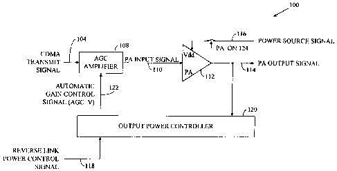
FIG. 1 illustrates an RF amplification circuit 100 in a wireless CDMA
telephone according to a preferred embodiment of the present invention. This
amplification circuit comprises several components. These components
include an automatic gain control (AGC) amplifier 108, a power amplifier (PA)
112, and an output power controller 120. Several signals are associated with
this amplification circuit. These signals include a CDMA transmit signal 104,
a
PA input signal 110, a PA output signal 114, a power source signal 116, a
reverse
link power control signal 118, an automatic gain control signal (AGC_V) 122,
and a PA_ON 124.
AGC amplifier 108 receives CDMA transmit signal 104 and amplifies it
according to an adjustable gain. In a preferred embodiment, this signal is at
a
fixed power level. This enables predictable performance of RF amplification
circuit 100. This amplified signal is output by AGC amplifier 108 as PA input
signal 110.
The gain of AGC amplifier 108 is controlled by automatic gain control
signal (AGC_V) 122. In a preferred embodiment, this signal is an electrical
voltage or current that can be varied to adjust the gain of AGC amplifier 108.
Increasing the voltage of analog control signal 122 also increases the gain of
CA 02376915 2001-12-12
WO 00/77950 PCT/US00/16269
AGC amplifier 108. In an alternate embodiment, the gain of AGC amplifier 108
can be controlled by a digital signal.
PA 112 is a power amplifier that amplifies PA input signal 110. This
amplified signal is output by PA 112 as PA output signal 114. In a preferred
5 embodiment, PA output signal 114 is directed to an antenna segment of a
CDMA phone for wireless transmission. PA 112 operates according to a fixed
gain. However, in alternate embodiments, PA 112 can have an adjustable gain.
The performance of PA 112 is typically measured by the power level of PA
output signal 110.
In a preferred embodiment, CDMA transmit signal, PA input signal 110,
and PA output signal 114 are all RF signals. In other words, these signals
exist
in the RF spectrum. However, in alternate embodiments, these signals could
exist in other frequency ranges.
As illustrated in FIG. 1, PA 112 accepts power source signal 116. In a
preferred embodiment, power source signal 116 is a direct current (DC)
voltage.
This voltage signal is also known as Vdd. Power source signal can be generated
by a battery or other external power source. Typical batteries include lithium-
ion and nickel-metal hydride batteries. Examples of external power sources
include car cigarette lighters, and household alternating current (AC) power
converted to a DC voltage. Power source signal 116 can be interrupted by
PA_ON 124. PA_ON 124 is a signal that is triggered when a wireless phone is
in standby mode. This interrupt capability reduces the current draw on power
sources, thereby conserving energy.
Output power controller 120 automatically controls the output power by
adjusting AGC_V 122. Specifically, output power controller 120 controls the
magnitude of AGC_V 122. In a preferred embodiment, output power
controller 120 accepts PA output signal 114, and reverse link power control
signal 118 as input signals. These input signals are then manipulated
according
a process described with respect to FIG. 3 to generate automatic gain control
signal (AGC_V) 122.
CA 02376915 2001-12-12
WO 00/77950 PCT/US00/16269
6
Output power controller 120 accepts PA output signal 114 to estimate the
power level of PA output signal 114. In a preferred embodiment, output power
controller also monitors signals representing ambient temperature and the DC
supply voltage. These signals are used by output power controller 120 to
determine a maximum allowable power level of PA output signal 114.
Output power controller 120 also accepts reverse link power control
signal 118 to perform in accordance with directives received from cellular
base
stations. Digital reverse link power control signal 118 is a digital signal.
In a
preferred embodiment, this signal is derived from directives received from a
cellular base station via a cellular network channel that is dedicated to
overhead traffic. These directives command a wireless phone to adjust the
power level of PA output signal 114. Output power controller 120 considers
these directives in conjunction with the determined maximum allowable
power level of PA output signal 114. A desired power level of PA output signal
114 results from this consideration. In an alternate embodiment, output power
controller 120 does not consider digital reverse link power control signal
118.
Instead, output power controller 120 equates desired power level to maximum
allowable power level. Output power controller 120 then converts this desired
power level into AGC_V 122 having the appropriate magnitude.
FIG 2 illustrates a battery discharge curve. This curve depicts the typical
decline of a battery's voltage over time as it supplies electrical current
necessary
to support wireless phone calls. This discharge curve profiles a time interval
when battery voltage declines from 4.1 Volts to 3.2 Volts. As illustrated by
this
curve, the battery's voltage is greater than 3.7 Volts for the majority of
this
interval. A battery's voltage also fluctuates according to temperature. In
general, as temperature increases, so does a battery's voltage.
Wireless telephones are capable of operating across a range of voltages.
However, for all wireless phones, there is a minimum operational voltage. If a
wireless phone's power source fails to supply power above this voltage, the
phone will not function properly. A typical minimum operational voltage for
CA 02376915 2001-12-12
WO 00/77950 PCT/US00/16269
7
CDMA wireless phones is 3.0 Volts. As illustrated by FIG. 2, if a wireless
phone
is powered by a battery, it will operate at voltages above this minimum
operational voltage for a significant amount of time.
When a wireless telephone is operating at voltages greater than the
minimum operational voltage, the particular operating voltage affects the
performance characteristics of RF amplification circuit 100. This principle is
evident when RF amplification circuit 100 is calibrated to generate PA output
signal 114 at a certain power level. For a given output power calibration, the
non-linear characteristics of RF amplification circuit 100 will increase as
the
operating voltage decreases. As discussed above, increased out of channel
distortion is a manifestation of an increase in non-linear amplification
characteristics.
FIGs. 3A, 3B, and 3C illustrate the spectral characteristics of PA output
signal 114 as a function of the power level of PA output signal 114 and RF
amplification circuit's 100 operating voltage. Each of these figures contains
three curves of solid lines. These curves represent the spectral
characteristics of
a PA output signal 114 when the operating voltage is either 3.2, 3.7, or 4.2
Volts.
Each of these solid line curves has a center lobe and two side lobes. The
center
lobes exist is the middle of the depicted spectrum and have a larger magnitude
than the side lobes that exist to the left and right of each center lobe. The
center
lobes represent the power of PA output signal 114 inside its designated RF
transmission channel. The side lobes represent the power of PA output signal
114 outside of its designated RF transmission channel. This indicates the
amount of out of channel distortion. In FIGs. 3A, 3B, and 3C, each center lobe
is
of equal magnitude. In contrast, the side lobe magnitudes vary according to
operating voltage. Thus, out of channel distortion varies according to
operating voltage.
Each of these figures also contains a dotted line curve. This dotted line
curve is the ACPR limit. As stated above, the spectral characteristics of PA
output signal 114 cannot exceed this limit. In particular, FIG. 3C shows that
as
CA 02376915 2001-12-12
WO 00/77950 PCT/US00/16269
8
operating voltage decreases, the out of channel distortion of PA output signal
114 increases and eventually exceeds the ACPR limit. For example, when the
operating voltage is either 4.2 Volts or 3.7 Volts, PA output signal 114 is
within
the ACPR limit. In other words, there is passing margin. However, when the
operating voltage is 3.2 Volts, PA output signal 114 exceeds the ACPR limit.
In
this situation, no passing margin exists.
When considering the characteristics described above in light of the fact
that operating voltages fluctuate, RF amplification circuit 100 must employ
techniques to ensure that ACPR limits are not exceeded at any operating
voltage.
A conventional technique for guaranteeing compliance with ACPR
requirements involves the static calibration of a wireless phone's
amplification
characteristics during production. This calibration technique involves
powering a phone with its minimum operational voltage and adjusting
AGC_V 122 so that PA output signal 114 yields the maximum possible power
without exceeding a specified ACPR limit at this minimum voltage. This
technique is termed static calibration because once AGC_V 122 is set, it will
not
be adjusted. Therefore, according to this technique, output power controller
120
merely provides a constant AGC_V 122.
Static calibration is performed at minimum operational voltage because
RF amplification circuit 100 is most susceptible to non-linear performance at
this voltage. However, static calibration is a less than optimal solution.
Since
the voltage of power source signal 116 is typically greater than the minimum
operating voltage, RF amplification circuit 100 is often capable of producing
a
higher power PA output signal 114 without exceeding a specified ACPR limit.
Therefore, in a preferred embodiment, output power controller 120
dynamically controls AGC_V 122 in a manner that enables RF amplifier circuit
100 to produce a maximum power with passing margin.
FIG. 4 illustrates output power controller 120 according to a preferred
embodiment. Output power controller 120 comprises several components.
CA 02376915 2001-12-12
WO 00/77950 PCT/US00/16269
9
These components include a power detector 404, an analog multiplexer 406, an
analog to digital (A/D) converter 408, a processor 410, a power limit register
412,
a linearizer 414, a digital to analog (D/A) converter 416, and a temperature
sensor 418.
Power detector 404 accepts PA output signal 114 and estimates the power
of this signal. In a preferred embodiment, power detector 404 can detect RF
power over a 30 dB range having an upper limit of 1 watt and a lower limit of
1
milliwatt. Power detector 404 also generates an analog signal that is
proportional to this power estimate. In a preferred embodiment, this analog
signal is a DC voltage that is linearly proportional to the power level of PA
output signal 114. Power detector 404 sends this analog signal to an input
port
on analog multiplexer 406. Power detector 404 can be implemented with analog
circuitry, digital processing algorithms, or any other power detection and
estimation means known to persons skilled in the relevant arts.
Temperature sensor 418 converts the ambient temperature of RF
amplification circuit 100 into a temperature signal 436. In a preferred
embodiment, this temperature signal is a DC voltage that is linearly
proportional to the ambient temperature. Temperature sensor 418 sends this
analog signal to an input port on analog multiplexer 406. An exemplary
temperature sensor 418 is a thermocouple.
Battery voltage signal 420 indicates the operating voltage of RF
amplification circuit 100. In a preferred embodiment, battery voltage signal
420
is simply the battery voltage. This voltage can be obtained by connecting
conductors to each battery terminal.
Analog multiplexer 406 has input ports to accept analog signals generated
by power detector 404 and temperature sensor 418. Analog multiplexer 406 also
has an input port to accept battery voltage signal 420. In a preferred
embodiment, analog multiplexer 406 time division multiplexes these signals
into a single output signal that is timed according to an input select signal
424.
Input select signal 424 is received from processor 410. This single output
signal
CA 02376915 2001-12-12
WO 00/77950 PCT/US00/16269
will be referred to as ADCIN_V 426. ADCIN_V 426 comprises information
regarding the power level of PA output signal 114, the ambient temperature of
RF amplification circuit 100, and battery voltage signal 420. Analog
multiplexer
406 sends ADCIN_V 426 to an input port of A/D converter 408.
5 A/D converter 408 accepts ADCIN_V 426 via an input port and converts
it into a composite data signal 428. Composite data signal 428 comprises three
distinct digital signals: TEMP_N, PO_N, and BATT_N. These three digital
signals quantitatively describe the power level of PA output signal 114, the
ambient temperature of RF amplification circuit 100, and the magnitude of
10 battery voltage signal 420. A/D converter 408 converts these analog signals
into
TEMP_N, PO_N, and BATT_N according to defined relationships. These
relationships are described below. In a preferred embodiment, A/D converter
408 uses eight bits to encode these digital signals. A/D converter 408 sends
these signals to processor 410 according to a standard computer bus
architecture.
In an alternate embodiment, these signals are sent to processor according to
any data interface known to persons skilled in the relevant arts.
FIG. 5 is a curve illustrating the relationship between BATT_N and
battery voltage signal 420 according to a preferred embodiment. BATT_N is a
quantized digital signal represented by eight bits. Battery voltage signal 420
is
represented in Volts. As illustrated, the relationship between BATT_N and
battery voltage signal 420 is essentially linear. However, in alternate
embodiments, this curve can have any shape.
FIG. 6 is a curve illustrating the relationship between PO_N and the
power level of PA output signal 114 according to a preferred embodiment.
PO_N is a quantized digital signal represented by eight bits. The power level
of
PA output signal 114 is represented in decibels with respect to a milliwatt
(dBm). As illustrated, PO_N increases exponentially with the power level of
PA output signal 114. However, this curve can have any shape.
FIG. 7 is a curve illustrating the relationship between TEMP_N and the
ambient temperature of RF amplification circuit 100 according to a preferred
CA 02376915 2001-12-12
WO 00/77950 PCT/US00/16269
11
embodiment. TEMP_N is a quantized digital signal represented by eight bits.
The ambient temperature of RF amplification circuit 100 is represented by
degrees Celsius. As illustrated, TEMP_N decreases monotonically as the
ambient temperature of RF amplification circuit 100 increases. However, this
curve can have any shape.
Processor 410 is any component that can perform algorithms. Processor
410 also contains memory for information access and storage. In a preferred
embodiment, processor 410 is a microprocessor. However, in alternate
embodiments, processor 410 may comprise processing capability dispersed
among one or more application specific integrated circuits (ASICs) or other
hardware capable of performing algorithms. Exemplary processors 410 include
reduced instruction set computer (RISC) processors, microcontrollers, finite
state machines, personal computer processors, and the mobile station modem
(MSM) chip. Processor 410 accepts TEMP_N, PO_N, and BATT_N from A/D
converter 408 and performs an algorithm that sets the maximum allowable
power level of PA output signal 114. This maximum allowable power level is
output by processor 410 as LIMIT_N 430. LIMIT_N 430 is an eight bit digital
signal sent to power limit register 412 according to a standard computer bus
architecture. In an alternate embodiment, LIMIT_N 430 is sent to power limit
register 412 according to any data interface known to persons skilled in the
relevant arts.
Processor 410 generates LIMIT_N 430 according to an algorithm. This
algorithm can be described at an abstract level with the following equation:
LIMIT_N = f(BATT_N, TEMP_N, PO_N, external power detected signal 422)
The above equation states that LIMIT_N 430 is determined according to a
mathematical function that is dependent on four signals: BATT_N, TEMP_N,
PO_N, and external power detected signal 422. Processor 410 can perform this
function through mathematical computation. However, in a preferred
CA 02376915 2001-12-12
WO 00/77950 PCT/US00/16269
12
embodiment, processor 410 performs this function by accessing a lookup table
containing pre-compiled values.
FIG. 8 is a flowchart illustrating a lookup table algorithm performed by
processor 410 according to a preferred embodiment. The algorithm begins with
step 804. In this step, processor 410 converts TEMP_N, PO_N, and BATT_N
into a lookup table address. Next, in step 806, processor 410 accesses the
contents of this lookup table address. The contents of this address specify
the
maximum achievable power level of PA output signal 114 that will satisfy
specified ACPR requirements. Step 808 is performed next. In step 808,
processor 410 converts the accessed table entry into LIMIT_N 430. As described
above, LIMIT_N 430 is a digital signal that can be represented by any number
of
bits.
The lookup table described above contains maximum power levels of PA
output signal 114 that satisfy a specified ACPR requirement. In a preferred
embodiment, each of these powers is based on a combination of temperature,
operating voltage, and the existing power level of PA output signal 114. The
contents of maximum power lookup table can be determined by empirical
methods. An exemplary empirical method comprises operating RF power
amplification circuit 100 at various combinations of temperature, operating
voltage, and PA output signal 114 power level to determine the maximum
achievable power level within ACPR limits for each combination. Once this
maximum power level is determined for a given combination, it is placed in
the lookup table described above. In a preferred embodiment, this lookup table
is stored in memory that is contained in processor 410.
In alternate embodiments, maximum power lookup table can store a
function that is based on a theoretical formula. An exemplary formula is
provided below:
LIMIT_N = max(min((a = BATT_N + b= TEMP_N + C= PO_N), d),e),
CA 02376915 2001-12-12
WO 00/77950 PCT/US00/16269
13
Where:
a, b, and c = a function or curve fit based on measured data from
RF amplification circuit 100;
d = a value equal to a minimum allowed power level of PA
output signal 114 to meet specified CDMA performance standards;
and
e = a value equal to a maximum allowed power level of PA output
signal 114 to meet FCC requirements.
FIG. 9 illustrates the relationship between power levels in decibels with
respect to a milliwatt (dBm) and LIMIT_N 430. As stated above, LIMIT_N 430
is a digital signal that quantitatively represents the maximum allowable power
level of PA output signal 114. In this figure LIMIT_N is a digital signal
represented by eight bits. In a preferred embodiment, the correspondence or
relationship between LIMIT_N units and the power level of PA output signal
114 in dBm is linear.
If RF amplification circuit 100 is powered by an external power source
such as a car cigarette lighter, External power detected signal 422 is
enabled.
Processor 410 monitors external power detected signal 422. If this signal is
enabled, processor 410 does not perform the algorithms described above.
Rather, processor 410 sets LIMIT_N 430 to a predetermined value. In a
preferred embodiment, this predetermined LIMIT_N 430 value is 255. When
using the relationship defined in FIG. 9, this value corresponds to a PA
output
signal 114 power level of 29 dBm.
As described above, power limit register 412 receives LIMIT_N 430, from
processor 410. Power limit register 412 also receives reverse link power
control
signal 118. Power limit register generates a dBm_N 432 signal and sends it to
linearizer 414. dBm_N is a digital signal that quantitatively represents the
desired power level of PA output signal 114. In a preferred embodiment,
dBm_N 432 is a digital signal represented by eight bits.
CA 02376915 2001-12-12
WO 00/77950 PCT/US00/16269
14
Power limit register 412 compares the values of LIMIT_N 430 and
reverse link power control signal 118. Based on this comparison, power limit
register 412 generates dBm_N 432 according to the following equation:
dBm_N = min(LIMIT_N, reverse link power signal 118)
Effectively, the output of power limit register 412 is the minimum of LIMIT_N
430 and reverse link power control signal 118.
Linearizer 414 translates the desired dBm_N 432 signal into an AGC_N
434 signal. AGC_N 434 is an initial representation of AGC_V 122. In a
preferred embodiment, AGC_N 434 is a digital signal represented by eight bits.
After being generated, AGC_N 434 is sent to D/A converter 416.
FIG. 10 illustrates the relationship between dBm_N 432 and AGC_N 434.
In a preferred embodiment, this relationship is substantially linear. However,
at higher dBm_N 432 levels, this relationship becomes non-linear. This non-
linearity is purposefully added to correct for non-linear characteristics of
AGC
amplifier 108. AGC amplifiers 108 often have unique non-linear
characteristics.
Therefore, the relationship between dBm_N 432 and AGC_N 434 must be
calibrated in each linearizer 414.
D/A converter 416 translates AGC N 434 into AGC V 122. AGC V 122
is a DC voltage that controls the gain of AGC amplifier 108. In a preferred
embodiment, CDMA transmit signal 104 has a fixed power level. Therefore,
the gain of AGC amplifier 108 is the only variable that controls the power
level
of PA output signal 114.
FIG. 11 is a curve illustrating the relationship between AGC_V 122 and
AGC_N 434. In a preferred embodiment, this curve is linear. However, in
alternate embodiments, this curve can have any shape.
FIG. 12 is a curve illustrating the relationship between PA input signal
110 and AGC_V 122. The curve is essentially linear. However, as AGC_V 122
CA 02376915 2001-12-12
WO 00/77950 PCT/US00/16269
increases, this relationship becomes non-linear. As discussed above with
respect to FIG. 10, these non linear characteristics are corrected by
linearizer 414.
While various embodiments of the present invention have been
described above, it should be understood that they have been presented by way
5 of example only, and not limitation. Thus, the breadth and scope of the
present
invention should not be limited by any of the above-described exemplary
embodiments, but should be defined only in accordance with the following
claims and their equivalents.
10 We claim: