Note: Descriptions are shown in the official language in which they were submitted.
v
~ CA 02376940 2002-03-15
HY Hwang 6-1 1
POLYCRYSTALLINE FERROELECTRIC
OPTICAL DEVICES
Field of the Invention
This invention relates generally to ferroelectric optical devices and, more
s particularly, to polycrystalline ferroelectric optical modulators.
Background of the Invention
Ferroelectric perovskite materials are well known for their utility in the
optoelectronics arf. Single crystal lithium niobate, for example, is used
commercially in
the design of external electro-optic modulators for laser transmitters. The
relatively large
electro-optic coefficient of single crystal barium titanate (8T0) makes this
material
especially well suited to similar applications. See, for example, M. Zgonik et
al., Phys. .
Rev. B, Vol. 50, pp. 59415949(1994), which is incorporated herein by
reference. Others
nave shown that single crystal thin films of BTO with good structural
properties can be
grown on magnesium oxide (Mg0) and other crystalline substrates using well-
known
pulsed laser deposition (PLD)techniques. See, respectively, L. Beckers et al.,
J. Appl.
Phys., Vol. 83, No. 6, pp. 3305-3310 (1998) and M. Siegert et al., Mat. Res
Soc. Symp.
Proc., Vol. 597, pp. 706-711 (2000), both which are also incorporated herein
by
reference.
It would be desirable to be able integrate this type of modulator into optical
zo ~ integrated circuits (OICs), in particular OICs fabricated using well-
known silicon-optical-
bench (SiOB) technology. In this technology, silica optical waveguides are
formed on a
single crystal silicon substrate. These waveguides are capable of guiding
optical
radiation at wavelengths of about 1100-1550 nm; and the design typically
endeavors to
minimize the amount of radiation that is coupled into the silicon substrate,
which has a
2s much higher refractive index (about 3.5) than that of silica (about 1.5) at
these
wavelengths. In one design, an epitaxial Mg0 optical isolation layer is formed
on the
silicon substrate to reduce the amount of radiation that is coupled into the
substrate. One
approach to incorporating an etectro-optic modulator into this design would be
to deposit,
CA 02376940 2002-03-15 '
HY Hwang Cr1 2
for example, single crystal BTO over the Mg0 layer. See, US Patent 6,103,008
issued to
R. A. McKee et at. on August 15, 2000. However, it is difficult to deposit
these layers on
a silicon substrate. First, to keep optical losses relatively lover the Mg0
and BTO layers
are made to be relatively thick. Second, the thermal expansion coefficients of
the layers
s are different from that of the silicon substrate. Third, the layers are
deposited at an
elevated temperature, and when they are cooled the combination of thick layers
and
different thermal expansion coefficients conspires to produce significant
strain, which in
turn causes the layers to crack.
Thus, a need remains in the art for an optical modulator design that would
allow
1o ferroelectric electro-optic materials to be more readily integrated into
OICs.
One approach might be to replace the electro-optic single crystalline layer
with a
polycrystalline layer. This design would simplify integration considerably;
the
deposition temperature could be lowered and the epitaxial isolation layer
could be
replaced by an amorphous silicon dioxide layer, thereby alleviating the
thickness
is constraints described above. Nevertheless, this approach is fraught with
difficulty too -
polycrystalline electro-optic materials tend to have disadvantageously high
optica!
scattering in the wavelength regime where the electro-optic coefficient is
high. See, for
example, B. Wong et al., J. Appl. Phys, Vol. 70, No. 3, pp. 1180-1184 (1991),
regarding
the Pocket's effect in polycrystalline ZnS planar waveguides and E. Dogheche
et al.,
20 lldicroelectronic Errgirteeri~rg, Vol. 29, pp. 315-318(1995) regarding the
optical
properties of lead-based ferroelectric thin films, both of which are
incorporated herein by
reference.
Summary of the Invention
In accordance with one aspect of our invention, an optical device comprises a
2s body of ferroelectric material exhibiting an effective electro-optic
coefficient (r~tr~) and an
optical loss (a), with the body being adapted for the propagation of optical
radiation at a
wavelength l~ through it, and means for applying an electric field to the body
in order to
alter the refractive index therein, characterized in that the body is
polycrystalline and has
an average grain size such that rt,~ is relatively high and a is relatively
low, both at a",. In
CA 02376940 2002-03-15
HY Hwang 6-1 3
a preferred embodiment the body has an average grain size that is less than
about ~i,° /10,
preferably in the range of approximately
8-20 nm, which is especially well suited for devices operating at near
infrared
wavelengths in the range of about 1000-1600 nm. Illustratively, the
ferroelectric body is
s a perovskite material such as BTO or lithium niobate.
As used herein the term ferroelectric material includes paraelectric materials
in
which the average grain size is so small that the material does not maintain a
spontaneous
polarization at zero applied field, yet it does exhibit a significant electro-
optic coefficient:
Brief Descriptiow of the Drawing
Io Our invention, together with its various features and advantages, can be
readily
understood from the following more detailed description taken in conjunction
with the
accompanying drawing, in which:
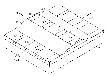
FIG. 1 is a schematic, isometric view of an optical modulator having a
multiplicity of waveguides in accordance with one embodiment of our invention;
1s FIG: 2 is a schematic graph of optical scattering loss (oco$ ) and
effective electro-
optic coei~icient (rQff) as a function of the characteristic dimension I,~
(e.g., average grain
size) of a crystal;
FIG. 3 shows x-ray diffraction (XRD) graphs of polycrystalline BTO films
deposited by PLD at various substrate temperatures ranging from 400° C
to 500° C. The
20 (200) peaks are evident;
FIG. 4 is a graph of refractive index at a wavelength of about 633 nm for both
TE
and TM modes versus growth temperature of amorphous and polycrystalline BTO
films.
The solid line is merely a guide to the eye;
FIG. 5 is a graph of optical loss for both TB and TM modes as a function of
2s waveguide width in an optical modulator of the type depicted in FIG. 1. In
this
embodiment the polycrystalline BTO layer was 120 nm thick and was deposited at
425°
C on silica waveguides;
CA 02376940 2002-03-15
HY Hwang b-1 4
FIG. 6 is a graph showing the response (transmitted optical intensity versus
applied electric field) for a modulator of the type described with reference
to FIGs. 1 & 5.
The response was measured for the lowest loss waveguide (i.e., the waveguide
with the
best mode field match to the optical fiber that delivered the input optical
signal) as the
s applied electric field was cycled from 300 V down to 0 V and back up to 300
V. The
inside edge-to-inside edge electrode spacing was 30 p,m; and
FIG. 7 is a graph showing the effective field-dependent electro-optic
coefficient.
The solid curve is for increasing electric field; the dashed curve for
decreasing electric
field.
In the interest of clarity and simplicity, FIGS. 1 & 2 have not been drawn to
scale.
Detailed Description of the Invention
General Discussion
With reference now to FIG. 1, an electro-optic modulator 10 comprises at least
one integrated optical waveguide 12.1 and a body 20 of polycrystalline
ferroelectric
Is material disposed so that at least a portion of the optical radiation
propagating in the
waveguide is coupled into the body 20. Illustratively, body 20 is formed on
top of
waveguide 12.1 as a trapezoidal-like prism having a flat top surface 20.3 and
slanted or
oblique side surfaces 20.1 and 20.2. The latter form tapered optical input and
output
couplers that facilitate coupling a portion of the radiation in waveguide 12.1
into and out
2o ofbody 20. Other optical couplers may also be used for this purpose (e.g.,
well-known
lateral waveguide couplers).
An electric field is applied to the body 20 by means of elongated electrodes
16.2
and 16.3, which are located on the top surface 20.3 of body 20 and straddle
the
underlying waveguide 12.1. This field alters the refractive index of the
ferroelectric body
2s and thereby alters or modulates a parameter (e.g., intensity, phase,
frequency) of the
optical radiation propagating through the modulator. This radiation is
illustratively
represented by an input optical signal 14.1 to be modulated, which is applied
to one end
of waveguide 12. l, and by a modulated output optical signal 14.2, which is
extracted
from the opposite end ofwaveguide 12.1.
CA 02376940 2002-03-15
HY Hwang 6..1 5
For purposes of illustration, and to demonstrate various aspects of modulator
performance discussed later, the modulator 10 is depicted as having three
integrated
waveguides 12.1 (described above), 12.2 and 12.3 each of different width, with
the latter
two waveguides being laterally disposed on opposite sides of waveguide 12_2.
Fewer
3 than three or more than three waveguides are contemplated by our invention.
In
conjunction with these waveguides, two additional electrodes 16. l and 16.4
are disposed
on top surface 20.3 of body 20, so that the four electrodes straddle the three
waveguides
as shown.
In as illustrative embodiment, the modulator includes a substrate 22, a layer
18
formed on the substrate, with the waveguides 12.1, 12.2 and 12.3 being formed
in layer
18. In a preferred embodiment, our modulator is constructed using well-known
silicon
optical bench (SiOB) technology in which substrate 22 is single crystalline
silicon, layer
18 is silicon dioxide (silica), waveguides 12.1-12.3 are doped silica,'and
body 20 is a
polycrystalline, ferroelectric material. Preferably the ferroelectric material
is a p~rovskite
is such as lithium niobate or BTO. An important aspect of our invention is the
ability to
control the average grain size of polycrystalline body 20 so that, at the
wavelength of the
input optical signal (e.g., 14.1), it exhibits a relatively high effective
electro-optic
coefficient reff while at the same time having relatively low optical optical
loss a. To
better appreciate the significance of this aspect, we turn to FIG. 2, which
shows
schematically how two parameters, electro-optic coefficient and optical
scattering loss
oc"S vary with a characteristic length l,K,a, (e.g., average grain size) of a
crystal. The solid
curve I represents the optical scattering loss and exhibits a peak when the
characteristic
length of the crystal is approximately equal to the wavelength ~ of the
optical signal
propagating in the crystal (i.e.; the crystal exhibits typical Raleigh
scattering): In contrast
2s the dashed curves II and III represent the effective electro-optic
coe~cient. Curve II
demonstrates that when l,~ is large relative to ~ there is no regime where r~~
is high and
simultaneously ocos is low. Thus, a modulator designed using such a material
would
either exhibit effective modulation with unacceptably high loss, or the
converse. On the
CA 02376940 2002-03-15
HY Hwang 6-1 6
other hand, curve III demonstrates that there is a regime or range R where
1,~~ is smaller
than ~ and where both of the desirable properties simultaneously exist: high
reff and low
ocos. In general, to ensure that a device operates in the latter regime 1,~1
should be less ' ,
than about a,o/10. Similar principles apply when one considers total optical
loss (a),
s which is a combination of optical scattering loss (oc~) and optical
absorption (aoa).
In a preferred embodiment of our invention, we believe that this range
corresponds to grain sizes of about 8-20 nm for polycrystalline ferroelectric
materials at
near infrared wavelengths of about 1000-1600 nm, and have specifically
demonstrated
this to be the case for polycrystalline BTO.
Example '
This example describes an electro-optic modulator in accordance with one
embodiment of our invention in which the waveguide structure is implemented
using
SiOB technology and the electro-optic modulating material comprises
polycrystalline
BTO. Various materials, dimensions and operating conditions are provided byway
of
Is illustration only and, unless otherwise expressly stated, are not intended
to limit the scope
of the invention. As used herein, the term undopeci means that a particular
layer or region
is not intentionally doped; i.e., any doping of such a region or layer is
relatively low and
typically results from residual or background doping in the chamber used to
deposit,
grow or otherwise form the layers of the device.
2o As shown in FIG. 1, we used well-known SiOB technology to fabricate the
underlying waveguide structure, which included an undoped, silica layer 18
deposited on
a single crystal, (100)-oriented, silicon substrate 22 and a multiplicity of
doped silica
waveguides 12.1-12.3 partially embedded in layer 18. The top, undoped silica
cladding
layer, which is typical of many SiOB designs, was omitted. The silica layer 18
was about
ZS 1 S ~m thick and was deposited by well-known high-pressure oxidation
(HZnOX). The
waveguides 12.1, 12.2 and 12.3 were all about 5 p,m deep, about 2 - 9 p,m wide
(but data
for only 2-8 itm are shown in FIG: 5), respectively, and were all lightly
doped with
phosphorus. Additional detail on SiOB technology can be found in the
literature; see, for
CA 02376940 2002-03-15
HY Hwang 6-I 7
example, Y. P. Li et al., Optical Fiber Communications, IIIB, edited by I. P.
Kaminow et
al., Ch. 8, Academic Press ( 1997), which is incorporated herein by reference.
A polycrystalline BTO layer, shaped into trapezoidal-like prism body Z0, was
deposited directly onto the top surface of both the silica waveguides 12.1-
12.3 and the
s silica layer 18, which are both amorphous. We used a well-known pulsed laser
deposition (PLD) technique to deposit the BTO. More specifically, the
substrates were
mounted on an inconel plate that was heated by a quartz lamp to temperatures
up to 900°
C. Prior to deposition, the chamber was evacuated to a pressure of about 10~
Pa. After
heating up the substrate to the desired growth temperature, an oxygen
atmosphere of
1o about 1 Pa was established in the chamber. To effect deposition a KrF
excimer laser
(e.g., a commercially available Lambda model LPX305) operating at a repetition
rate of
about 20 Hz was focused onto a sintered disc of BTO. Under these conditions an
energy
density of approximately 3 J/cm2 was created in the disc. The substrate (i.e.,
the silicon
substrate with silica. waveguides thereon) target distance was set to about 7
cm, which
1s resulted in a deposition rate of about 0.4 nm/s.
The oblique surfaces 20.1 and 20.2 of the tapered couplers were realized by
covering the ends of the substrate with shadow masks. For our deposition
parameters, a
substrate-to-shadow-mask distance of about 4 mm generated about 3 mm long
ramps.
Finally, Cr/Au rectangular electrodes 16-1-16.4 were deposited and patterned
using
2o standard deposition, photolithography and lift-offtechniques. The electrode
dimensions
were as follows: inside edge-to-inside edge spacing of about 30 mm; length of
about 5
mm; and width of about 50 pm or 100 p,m.
We structurally characterized our BTO layers using Rutherford Backscattering
Spectrometry (RBS) and x-ray diffraction (XRD). The composition and thickness
of the
2s deposited BTO layers were measured with RBS using 2 MeV He* ions. The Ba:Ti
ratio
was found to be essentially l : l within the measurement resolution.
For these measurements, the BTO layers were uniformly about 400 nm thick (no
tapered couplers were formed) and were deposited at temperatures ranging from
400° C
- CA 02376940 2002-03-15
HY Hwang 6-1 8
to 500° C. These layers were investigated by means of XRD. XRD pole
figure studies
(not shown) demonstrated that the BTO layers were only weakly textured with a
< 100>
preference.
The (200) peak of the 6-28 scans is also shown in FIG. 3. The build up and
s sharpening of these peaks v~ith increasing growth temperature provoked a
clearly visible
transition from amorphous (about 400° C) to polycrystalline (above
about 413° C). The
FWHM of the peak were determined and the grain sizes were calculated using
well-
known Schemer's formula:
d = (~~COSB (1)
where d is the average grain size of the polycrystalline BTO, K = 0.89 and is
a geometric
factor,
~,x is
the x-ray
wavelength,
W is the
width of
the (200)
peak at
FWHM, and
A is
the position The measured
of the data is
(200) peak. shown
in the
table
below:
TEMP (Cj 28 () W() a (n~)
500 44.23 0.48 17.73
450 44.33 0.46 18.50
438 44.29 0.69 12.23
425 44.23 0.84 10.13
413 44.48 0.87 9.78
400 ___ ___ ___
This data shows that average grain sizes of about 9.8 nm to 18.5 nm were
realized with
PLD growth of polycrystalline BTO at temperatures in the range of about 413-
500° C.
1s At about
500° C the grain size reached the resolution limit of our x-ray
equipment, but we expect
that the average grain size would continue to increase as the temperature is
increased
above 500° C. This table, and other data not shown, demonstrate an
acceptable average
grain size range of about
10 8-20 nm, which is particularly well suited for use in devices that operate
at near infrared
wavelengths of about 1000-1600 nm.
CA 02376940 2002-03-15
HY Hwang 6-1 9
Optical characterization included measurement of the refractive index of the
BTO
layers (FIG. 4), the optical loss of these layers (FIG. 5), the modulator
response (FIG. 6),
and the electro-optic coefficient of the BTO layers (FIG. 7). More
specifically, the
refractive index and thickness of the BTO layers were measured at a wavelength
of about
S 633 nm using a prism setup of the type described by L. Beckers et al.,
supra. The results
are shown in FIG. 4. For samples grown atabout 400° C and about
413° C, only the T1VI
modes could be measured. The amorphous sample grown at about 400° C
exhibited a
refractive index of only about 2.0, but the index increased at higher growth
temperatures
where the layers became polycrystalline: at about 413° C the index was
about 2.25 and at
1o about 450° C is was above about 2.3 (nearly the value of bulk BTO
single crystalline
material; i.e., 2.41 and 2.36 for ordinary and extraordinary rays,
respectively). This trend
of increasing index with increasing temperature corresponds to increasing
average grain
size with increasing temperature.
Next, a simple loss measurement was performed. The 1.54 pm output from a
1s fiber-coupled diode laser was butt-coupled from a S pm core standard fiber
into and out
of each of the modulator waveguides (e.g.; 12.1-12.3, although in this case
the device had
7 waveguides with widths of 2, 3, 4, 5, 6, 7 and 8 p,m). The input tapered
coupler
coupled a portion of the input signal 14.1 into the BTO body 20 due, in part,
to the fact
that it has a higherrefractive index (2,3) than that of the underlying silica
waveguide
2o (1.5). Then the signal propagated through the body 20 being guided by the
underlying
silica waveguide (like a strip-loaded waveguide). The output tapered coupler
coupled the
signal back into the silica waveguide 1 Z.1 where it emerged as output signal
14.2. The
optical intensity of output signal 14.2 was measured with a fiber power meter.
Zero dB
was calibrated to the intensity delivered when the fibers were butt-coupled to
one another
2s (i.e., there was no silica waveguide between them). FIG. S shows the
measured optical
loss as a function of silica waveguide width ranging from 2-8 p,m. The BTO
layer
overlying all 7 of these waveguides was about 120 nm thick in its flat central
section and
was deposited at about 425° C. The length of the tapered couplers
(i.e., the length of the
CA 02376940 2002-03-15
HY Hwang 6-1 10
slanted surfaces 20. l and 20.2 shown in FIG. 1 ) was about 3 mm. The minimum
loss,
about - 1.5 dB for TE modes and about - 2.5 dB for TM modes, was achieved for
waveguide widths of 3-5 pm, which had the best mode field match to the optical
fiber
that delivered the input optical signal to the modulator. Below this range
(i.e., for 2 p,m
s wide waveguides) the optical loss was dominated by radiation lost in
coupling from the
input fiber to the silica waveguide, whereas above this range (i.e:, for 3-9
p,m wide
waveguides) the optical loss was dominated by radiation lost in coupling from
the silica
waveguide to the output fiber.
For BTO layers thicker than about 1 SO nm, the underlying silica waveguide
1o guides the optical signal too weakly to ensure low loss propagation through
the device;
i.e., the signal is scattered into adjoining waveguides. Thicker BTO layers
could be
realized by forming a shallow BTO rib on the BTO layer and over the underlying
silica
waveguide, a design that is akin to well-know ridge waveguide structures. In
this
embodiment we expect the loss to be reduced to less than. about 1 dB/cm due to
the
Is reduced surface scattering.
In order to make electro-optic measurements on our modulator, we used the
following set up (not shown): the optical input signal to one of the silica
waveguides was
delivered by a
1.54 pm semiconductor diode laser. The output of the laser was passed through
a fiber
2o polarizer in order to adjust the polarization of the input signal to be
about 45° with
respect to the normal to the top surface of the modulator. Thus, both the TE
and TM
modes were~launched in phase and with essentially equal intensities into the
waveguide:
However, the different propagation constants of these modes resulted in a
phase
difference between them at the output end of the waveguide. Consequently, the
output
2s signal was elliptically polarized. This optical output signal was focused
by a microscope
lens, passed through a polarizer set at about - 45°, and made incident
on a photodetector.
As the electric field applied to the modulator was changed, the refractive
indices of both
modes also changed, but by different amounts, which meant that phase
difference
CA 02376940 2002-03-15
HY Hwang 6-1 , 11
between the modes also changed. When the phase difference was equal to 0 or n,
the
intensity at the photodetector was a minimum or a maximum, where the phase
difference
r is given by:
r= ro - (~b)(rrs nra3 - rrM nrM3)ELe
s where ra = lco(n~ - n~Ld is the phase difference without an applied field,
lco = 2~ is
the propagation constant, ?~,o is the center wavelength of the input optical
signal, n~ and
n.~ are the refractive indices of the TE and TM modes, respectively, La is the
physical
length of the modulator measured from input to output, Lo is the length of the
electrodes
measured in the direction of signal propagation, and E is the amplitude of the
applied
to electric field.
With our experimental set up it was not possible to measure r.,$ and r~
independently, but we were able to measure an effective electro-optic
coefficient r~
given by:
re ff= r.~ _ n.~3/n.~3r.~ ' ~3)
1s The response of the modulator was taken in the following manner: Prior to
the
measurement, the BTO layer was poled for several minutes at 300 V resulting in
an
electric field of 10 V/cm. After the poling was completed, the voltage was
gradually
lowered down to 0 V in 91 steps each 100 ms long. We refer to this process as
a
downward scan. Then the voltage was step-wise increased to 300 V again in the
same
2o fashion. We refer to this as an upward scan. The resulting intensity of the
output optical
signal was measured and the transmitted intensity was plotted versus electric
field for
both scans, as shown in FIG. 6: For these measurements the length of the
electrodes was
about 5 mm and their inside edge-to-inside edge spacing was about 30 Nxn.
FIG. 6 also demonstrates that the modulator exhibited hysteretic behavior;
i.e., the
Zs curve for the downward scan (solid line) is shifted with respect to the
curve for the
upward scan (dashed line). Significantly, both scans clearly show a quadratic
behavior at
low to intermediate fields of less than about 5 V/ N.m. Only at relatively
high fields of
about 5-10 V/ pm did we observe a linear electro-optic erect. This effect
could be
CA 02376940 2002-03-15
HY Hwang 6-1 12
explained by the loss of net poling at low electric fields. It is very likely
that the
crystallites are too small to sustain a remnant polarization: Without an
external field no
internal polarization remains. An external field creates a polarization and
the electro-
optic effect becomes visible. The effective electro-optic coe~cients are
plotted in FIG. 7
s for both scans.
At fields of approximately 8 V/ p.m an effective electro-optic coefficient in
excess
ofabout 20 pm/V (e.g., reff~ 24 pm/V) was achieved at an optical loss below
about 1.5
dB
(e.g., 1.4 dB), which is extremely attractive especially when combined with
the
Io advantages of being able to build a modulator with polycrystalline
material.
It is to be understood that the above-described arrangements are merely
illustrative of the many possible specific embodiments that can be devised to
represent
application of the principles of the invention. Numerous and varied other
arrangements
can be devised in accordance with these principles by those skilled in the art
without
15 departing from the spirit and scope of the invention. In particular,
although we have
focused on modulator applications, it will be apparent that other optical
devices (e.g.,
tunable attenuators, optical switches, tunable couplers, and poled
ferroelectrics for
frequency shifters) could benefit from the use of polycrystalline,
ferroelectric materials in
their design.