Note: Descriptions are shown in the official language in which they were submitted.
CA 02377532 2001-12-17
1
SPECIFICATION
WAVEGUIDE GROUP BRANCHING FILTER
TECHNICAL FIELD
The present invention relates to a waveguide group branching filter
that is used mainly in VHF, UHF, microwave and millimeter wave bands.
TECHNICAL FIELD
Fig. 1 is a perspective view showing a conventional waveguide group
branching filter set forth, for example, in J. Bornemann, U. Rosenberg,
"Waveguide Components for Antenna Feed Systems: Theory and CAD,"
ARTECH HOUSE INC., pp. 413-418, 1993. In Fig. 1, reference numeral 61
denotes a square main waveguide; 62a denotes coupling holes of the same
shape formed through two opposed side walls of the square main waveguide
61 in symmetrical relation to each other; and 62b denotes coupling holes of
the same shape formed symmetrically through two other opposed side walls
of the square main waveguide 61 than those through which the coupling holes
62a are formed.
Furthermore, in Fig. 1, reference numeral 63a denotes two waveguide
low-pass filters that branch off via the coupling holes 62a from longitudinal
axis of the square main waveguide 61 at right angles to the axis thereof; and
63b denotes two waveguide low-pass filters that branch off via the coupling
holes 62b from the square main waveguide 61 at right angles to the axis
thereof. Reference numeral P1 denotes an input port of the square main
waveguide 61; P2 denotes an output port of the square main waveguide 61;
and 64 denotes a waveguide high-pass filter connected to the output port P2
CA 02377532 2001-12-17
2
and formed by two square waveguide steps.
Next, the operation of the prior art example will be described below.
Now, assume that a total of four kinds of radio waves, two orthogonal
polarized waves in each of two different frequency bands, are incident via the
input port P1 of the square main waveguide 61. The fundamental mode of
that one of the radio waves in the lower frequency band whose polarization
plane is vertical to the longitudinal axis of the waveguide low-pass filter
63a,
that is, the TE10 mode, undergoes total reflection due to the cutoff effect of
the waveguide high-pass filter 64 to form a standing wave in the square main
waveguide 61, which couples equally with the fundamental modes of the
opposed waveguide low-pass filters 63a through the coupling holes 62a and
propagates in the waveguide low-pass filters 63a.
The fundamental mode of the radio wave in the lower frequency band
whose polarization plane is vertical to the longitudinal axis of the waveguide
low-pass filter 63b, that is, the TE01 mode, undergoes total reflection due to
the cutoff effect of the waveguide high-pass filter 64 to form a standing wave
in the square main waveguide 61, which couples equally with the fundamental
modes of the two opposed waveguide low-pass filters 63 through the coupling
holes 62b and propagates in the waveguide low-pass filters 63b. Further, the
two radio waves of orthogonal polarization planes in the higher frequency
band among the four kinds of incident radio waves scarcely couple with the
coupling holes 62a and 62b due to the cutoff effect of the waveguide low-pass
filters 63a and 63b, and they propagate in the waveguide high-pass filter 64,
thereafter being emitted from the output port P2.
Suitable selection of the sizes and positions of the coupling holes 62a
and 62b allows effective suppression of the reflection of the radio waves in
the lower frequency band which are incident from the input port P1, and
CA 02377532 2001-12-17
3
suitable selection of the waveguide diameter of each step and the step spacing
of the waveguide high-pass filter 64 allows effective suppression of the
reflection of the radio waves in the higher frequency band which are incident
from the input port P1.
Since the conventional waveguide group branching filter has such a
structure as described above, even if the two frequency bands incident from
the input port P1 are widely spaced apart, vertical and bilateral symmetry of
the circuit configuration completely suppresses the generation of a high-order
mode which contributes greatly to unnecessary coupling of coupling holes,
such as the TE11 or TMll mode, in the branch section in the square main
waveguide 61 (in the neighborhood of the coupling holes 62a and 62b)--this
permits realization of a high-performance waveguide group branching filter
with highly excellent reflection and polarized waves isolation
characteristics.
The conventional waveguide group branching filter has such a
construction as described above, and hence it requires a combiner circuit (not
shown) for combining radio waves of the same polarization separated
between the two opposed waveguide low-pass filters 63b and a combiner
circuit (not shown) for combining radio waves of the same polarization
similarly separated between the two waveguide low-pass filters 63b;
accordingly, the entire circuit structure is very bulky and is difficult of
miniaturization. Moreover, because of its cubic structure, the integral
formation of respective components is not easy, giving arise to the problem of
di~culty in the reduction of manufacturing costs.
The present invention is intended to solve such a problem as
mentioned above, and has for its obj ect to provide a high-performance
waveguide group branching filter that can be made smaller and cheaper.
CA 02377532 2004-07-27
4
DISCLOSURE OF THE INVENTION
In accordance with one aspect of the present invention there is
provided a waveguide group branching filter comprising: a circular-to-
square waveguide multistage transformer connected to an input port; a
branch waveguide polarizerlbranching filter connected to said circular-to-
square waveguide multistage transformer; a first waveguide frequency filter
connected to a branching end of said branch waveguide polarizer/branching
filter; a rectangular waveguide H-plane T-branch circuit; a rectangular
waveguide multistage transformer operably connecting one end of said
CA 02377532 2004-07-27
S
branch waveguide polarizer/branching filter to said rectangular waveguide
H-plane T-branch circuit; a second waveguide frequency filter connected to
said rectangular waveguide H-plane T-branch circuit; and a third waveguide
frequency filter connected to said rectangular waveguide H-plane T-branch
circuit; wherein: a first radio wave of a first frequency band which has the
polarization plane perpendicular to a branch plane of said waveguide
polarizer/branching filter, a second radio wave of said first frequency band
which has the polarization plane parallel to the branch plane of said branch
CA 02377532 2004-07-27
6
waveguide polarizer/branching filter, and a third radio wave of a second
frequency band higher than said first frequency band which has the same
polarization plane as that of said first radio wave are incident to said input
port; and said first radio wave is cut off by said first and second waveguide
frequency filters and is emitted from said third waveguide frequency filter,
said second radio wave is cut off by said rectangular waveguide multistage
transformer and is emitted from said first waveguide frequency filter, and
said third radio wave is cut off by said first and third waveguide frequency
CA 02377532 2004-07-27
7
filters and is emitted from said second waveguide frequency filter.
In accordance with another aspect of the present invention there is
provided a waveguide group branching filter comprising: a bore within a
solid metal block, the bore including portions of varying shapes including, a
transforming portion configured to receive a plurality of radio waves from
an input port and transform the received radio waves from modes
compatible with circular waveguides to modes compatible with rectangular
waveguides; a branching portion operably connected to the multistage
CA 02377532 2004-07-27
portion; and a plurality of waveguide filtering portions operably connected
to the branching portion, wherein the branching portion is configured to
route the transformed radio waves to the waveguide filtering portions, the
waveguide filtering portions being configured to emit each of the
transformed radio waves through a corresponding one of a plurality of
output ports.
In accordance with yet another aspect of the present invention there is
provided a method of manufacturing a waveguide group branching filter,
CA 02377532 2004-07-27
9
comprising: boring surfaces of each of two metal blocks, wherein a circuit
structure is formed by the two bored surfaces, when the metal blocks are
assembled together, the circuit structure being operable to receive a
plurality
of radio waves, transform the received radio waves from modes compatible
with circular waveguides into modes compatible with rectangular
waveguides, and filtering the transformed radio waves, and emitting each
filtered radio wave from a corresponding one of a plurality of output ports.
CA 02377532 2004-07-27
BRIEF DESCRIPTION OF THE DARWINGS
Fig. 1 is a diagrammatic sketch of a conventional waveguide group
branching filter.
Fig. 2 is a diagrammatic showing of a waveguide group branching
Elter according to Embodiment 1 of the present invention.
Fig. 3 is a diagrammatic showing of a waveguide group branching
filter according to Embodiment 2 of the present invention.
Fig. 4 is a diagrammatic showing of a waveguide group branching
Elter according to Embodiment 3 of the present invention.
Fig. 5 is a diagrammatic showing of a waveguide group branching
alter according to Embodiment 4 of the present invention.
Fig. 6 is a diagrammatic showing of a waveguide group branching
filter according to Embodiment 5 of the present invention.
Fig. 7 is a diagrammatic showing of a waveguide group branching
filter according to Embodiment 6 of the present invention.
Fig. 8 is a diagrammatic showing of a waveguide group branching
filter according to Embodiment 7 of the present invention.
Fig. 9 is a diagrammatic showing of a waveguide group branching
filter according to Embodiment 8 of the present invention.
Fig. 10 is a diagrammatic showing of a waveguide group branching
alter according to Embodiment 9 of the present invention.
Fig. 11 is a diagram showing the relationship between post-type
v CA 02377532 2001-12-17
11
coupling holes and rectangular cavity resonators in a waveguide band-pass
filter according to Embodiment 9 of the present invention.
Fig. 12 is a diagrammatic showing of a waveguide group branching
filter according to Embodiment 10 of the present invention.
Fig. 13 is a diagram showing the relationship between
double-post-type coupling holes and rectangular cavity resonators in a
waveguide band-pass filter according to Embodiment 10 of the present
invention.
Fig. 14 is a diagrammatic showing of a waveguide group branching
filter according to Embodiment 11 of the present invention.
BEST MODE FOR CARRYING OUT THE INVENTION
To facilitate a better understanding the present invention, a description
will hereinafter be given, with reference to the accompanying drawings, of the
best mode for carrying out the invention.
EMB ODIIuVIENT 1
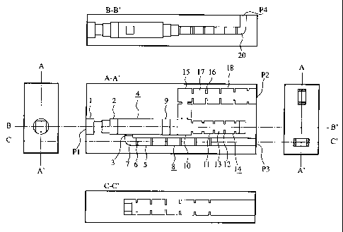
Fig. 2 is a diagrammatic showing of a waveguide group branching
filter according to Embodiment 1 of the present invention. In Fig. 2,
reference numeral 1 denotes a circular-to-square waveguide multistage
transformer; 2 denotes a square waveguide connected to one end of the
circular-to-square waveguide multistage transformer 1; 3 denotes a coupling
hole formed through one sidewall of the square waveguide 2; 4 denotes a
branch waveguide polarizer/branching filter formed by the square waveguide
2 and the coupling hole 3; S denotes a rectangular waveguide connected to the
branching end of the branch waveguide polarizer/branching filter and having
an E-plane bend; 6 denotes n (where n is an integer equal to or greater than 1
)
iris-type coupling holes provided in the rectangular waveguide 5; 7 denotes n
CA 02377532 2001-12-17
12
rectangular cavity resonators separated by the coupling hole 3 and the n
coupling holes 6 in the rectangular waveguide 5; and 8 denotes generally a
waveguide band-pass filter (a first waveguide band-pass filter) made up of the
rectangular waveguide S, the coupling hole 3, the iris-type coupling holes,
and
the rectangular cavity resonators 7.
In Fig. 2, reference numeral 9 denotes a rectangular waveguide
multistage transformer connected to one end of the branch waveguide
polarizer/branching filter; 10 denotes a rectangular H-plane T-branch circuit
connected to the rectangular waveguide multistage transformer 9; 11 denotes
a rectangular waveguide connected to one end of the rectangular waveguide
H-plane T-branch circuit 10; 12 denotes m+1 (where m is an integer equal to
or greater than 1) iris-type coupling holes provided in the rectangular
waveguide 11; 13 denotes m rectangular cavity resonators separated by the
m+1 iris-type coupling holes 12 in the rectangular waveguide 11; 14 denotes
generally a waveguide band-pass filter (a second waveguide band-pass filter)
made up of the rectangular waveguide 11, the iris-type coupling holes 12, and
the rectangular cavity resonators 13.
Furthermore, in Fig. 2, reference numeral 15 denotes a rectangular
waveguide connected to the branching end of the rectangular H-plane
T-branch circuit 10 and having an H-plane corner portion; 16 denotes n+1
iris-type coupling holes provided in the rectangular waveguide 15; 17 denotes
n rectangular cavity resonators separated by the n+1 iris-type coupling holes
16 in the rectangular waveguide 15; 18 denotes generally a waveguide
band-pass filter (a third waveguide band-pass filter made up of the
rectangular
waveguide 15, the iris-type coupling holes 16 and the rectangular cavity
resonators 17; 20 denotes a rectangular waveguide E-plane bend connected to
the waveguide band-pass filter 14; P1 denotes an input port; and P2 and P3
CA 02377532 2001-12-17
13
denotes output ports.
Next, the operation of this embodiment will be described below.
Now, assume that a radio wave V 1 (a first radio wave) of the
polarization plane vertical to the branch plane of the branch waveguide
polarizer/branching filter 4 in a certain frequency band fl (a first frequency
band), a radio wave H1 (a second radio wave) of the polarization plane
parallel to the branch plane of the branch waveguide polarizer/branching
filter
4 in the frequency band fl, and a radio wave V2 (a third rave wave) of the
same polarization plane as that of the radio wave in a frequency band t2 (a
second frequency band) higher than the frequency band fl, are incident from
the input port Pl. At this time, the incident radio wave V1 passes through
the circular-to-square waveguide multistage transformer 1, by which it is
transformed to the fundamental mode of the square waveguide 2, that is,
TE10 mode.
The radio wave V1 thus transformed to the TE10 mode does not
couple with the coupling hole 3 in the branch waveguide polarizer/branching
filter 4 due to the cutoff effect of the waveguide band-pass filter 8, but
instead
it propagates through the rectangular multistage transformer 9, then forms a
standing wave in the rectangular waveguide H-plane T-branch circuit 10 due
to the cutoff effect of the waveguide band-pass filter 14, couples with the
fundamental mode of the rectangular waveguide 15 via the iris-type coupling
holes 16, and passes through the waveguide band-pass filter 18, thereafter
being emitted from the output port P2.
Another incident radio wave Hl passes through the circular-to-square
waveguide multistage transformer l, by which it is transformed to the
fundamental mode of the square waveguide 2, that is, the TE01 mode. In the
branch waveguide polarizerlbranching filter 4 the radio wave Hl thus
CA 02377532 2001-12-17
14
transformed to the TE01 mode undergoes total reflection to form a standing
wave due to the cutoff effect of the square waveguide multistage transformer
9, then couples with the fundamental mode of the square waveguide 5 through
the coupling hole 3, and passes through the waveguide band-pass filter 8,
thereafter being emitted from the output port P3.
Yet another incident radio wave V2 pass through the circular-to-square
multistage transformer 1, by which it is transformed to the fundamental mode
of the square waveguide 2, that is, the TE10 mode. The radio wave V2 thus
transformed to the TE10 mode does not couple with the coupling hole 3 due
to the cutoff effect of the waveguide band-pass filter 8, but instead it
propagates through the rectangular waveguide multistage transformer 9; and
in the rectangular waveguide H-plane T-branch circuit 10, the radio wave
does not couple with the iris-type coupling holes 16 due to the cutoff effect
of
the waveguide band-pass filter 18, but it passes through the waveguide
band-pass filter 14 and the rectangular waveguide E-plane bend 20, thereafter
being emitted from the output port P4.
By suitably selecting the waveguide diameter of each step and step
spacing of each of the circular-to-square multistage transformer 1 and the
rectangular waveguide multistage transformer 9 and the size and position of
each of the coupling hole and the rectangular waveguide H-plane T-branch
circuit 10, reflected waves of the radio waves V1, H1 and V2 incident from
the input port P1 can be held small.
As described above, according to Embodiment l, even if the
frequencies of the radio waves Vl (H1) and V2 incident from the input port
P1 are widely spaced apart (f2>_~xfl), the generation of higher mode, which
greatly contributes to unnecessary coupling of polarized waves, typified by
the TE11 or TM11 mode, is completely suppressed in the square waveguide 2
CA 02377532 2001-12-17
by the vertical symmetry (symmetry to the A-A' plane in Fig. 2) of each of the
circular-to-square waveguide multistage transformer 1, the branch waveguide
polarizer/branching filter 4 and the rectangular waveguide multistage
transformer 9; therefore, this embodiment permits realization of a
5 high-performance waveguide group branching filter with very excellent
reflection and polarized wave isolation characteristics.
Further, according to Embodiment 1, the above-mentioned waveguide
group branching filter has a pseudo-planar circuit structure which needs only
to be divided into two along the A-A' plane in Fig. 2 so that all the
constituent
10 circuits can be formed by boring two metal blocks from their surfaces--this
facilitates miniaturization and cost reduction of the waveguide group
branching filter.
EMBODaVtENT 2
15 Fig. 3 is a diagrammatic showing of a waveguide group branching
filter according to Embodiment 2 of the present invention. In Fig. 3,
reference numeral 21 denotes two coupling holes formed through one side
wall of the square waveguide 2; and 22 denotes generally a branch waveguide
polarizer/branching filter formed by the square waveguide 2 and the two
coupling holes 21.
While Embodiment 1 is provided, as depicted in Fig. 2, with the
branch waveguide polarizer/branching filter 4 composed of the square
waveguide 2 and the single coupling hole 3, Embodiment 2 is provided, as
depicted in Fig. 3, with the branch waveguide polarizerJbranching filter 22 in
place of the branch waveguide polarizer/branching filter 4 shown in Fig. 2;
however, this embodiment is identical in construction with Embodiment 1 of
Fig. 2 except the above.
CA 02377532 2001-12-17
16
The radio waves V1 and V2 incident from the input port Pl do not
couple with the two coupling holes 21 in the branch waveguide
polarizer/branching filter 22 having the two coupling holes 21 due to
increased cutoff effect of the waveguide band-pass filter 8, but instead they
propagate in the square waveguide multistage transformer 9.
As described above, Embodiment 2 permits realization of a
high-performance waveguide group branching filter that has very excellent
reflection and polarized wave isolation characteristics in the square
waveguide 2 due to the vertical symmetry of the structures of the circular-to
square waveguide multistage transformer l, the branch waveguide
polarizer/branching filter 22 and the rectangular waveguide multistage
transformer 9.
Further, according to Embodiment 2, the cutoff effect of the
waveguide band-pass filter 8 against the radio waves V1 and V2 in the branch
waveguide polarizer/branching filter 22 having the two coupling holes 21 is
heightened--this permits realization of a lugh-performance waveguide group
branching filter of more excellent reflection and polarized waves isolation
characteristics.
Moreover, according to Embodiment 2, the waveguide group
branching filter has a pseudo-planar circuit structure which needs only to be
divided into two along the A-A' plane in Fig. 3 so that all the constituent
circuits can be formed by boring two metal blocks from their surfaces--this
facilitates miniaturization and cost reduction of the waveguide group
branching filter.
EMBODIIUVIEEN'T 3
Fig. 4 is a diagrammatic showing of a waveguide group branching
CA 02377532 2001-12-17
17
filter according to Embodiment 3 of the present invention. In Fig. 4,
reference numeral 23 denotes a thin metal sheet inserted in the square
waveguide 2; and 24 denotes generally a branch waveguide
polarizer/branching filter made up of the square waveguide 2, the single
coupling hole 3 and the thin metal sheet 23.
While Embodiment 1 is provided, as depicted in Fig. 2, with the
branch waveguide polarizer/branching filter 4 composed of the square
waveguide 2 and the single coupling hole 3, Embodiment 3 is provided, as
depicted in Fig. 4, with the branch waveguide polarizer/branching filter 24 in
place of the branch waveguide polarizer/branching filter 4 shown in Fig. 2;
however, this embodiment is identical in construction with Embodiment 1 of
Fig. 2 except the above.
The radio wave Hl incident from the input port P1 forms a standing
wave due to the cutoff' effect by the thin metal sheet 23, then couples with
the
fundamental mode of the square waveguide 5 through the coupling hole 3,
and propagates through the waveguide band-pass filer 8, thereafter being
emitted from the output port P3. The frequency characteristic by the cutoff
effect of the tlun metal sheet 23 is more stable than the frequency
characteristic by the cutoff effect of the square waveguide multistage
transformer 9--this provides excellent reflection and polarized waves
isolation
characteristics over a wider band.
As described above, Embodiment 3 permits realization of a
high-performance waveguide group branching filter that has very excellent
reflection and polarized wave isolation characteristics in the square
waveguide 2 due to the vertical symmetry of the structures of the circular-to
square waveguide multistage transformer 1, the branch waveguide
polarizer/branching filter 24 and the rectangular waveguide multistage
CA 02377532 2001-12-17
18
transformer 9.
Further, Embodiment 3 permits realization of a high-performance
waveguide group branching filter with excellent reflection and polarized
waves isolation characteristics over a wider band since the frequency
characteristic by the cutoff effect of the thin metal sheet 23 for the radio
wave
H1 is stable.
Moreover, according to Embodiment 3, the waveguide group
branching filter has a pseudo-planar circuit structure which needs only to be
divided into two along the A-A' plane in Fig. 4 so that all the constituent
circuits, except the thin metal sheet 23, can be formed by boring two metal
blocks from their surfaces--this facilitates miniaturization and cost
reduction
of the waveguide group branching filter.
EMBODIZUVIENT 4
Fig. 5 is a diagrammatic showing of a waveguide group branching
filter according to Embodiment 4 of the present invention. In Fig. 5,
reference numeral 25 denotes generally a branch waveguide
polarizer/branching filter made up of the square waveguide 2, the two
coupling holes 3 formed side by side through one side wall of the square
waveguide 2 and the thin metal sheet 23 inserted in the square waveguide 2.
While Embodiment 1 is provided, as depicted in Fig. 2, with the
branch waveguide polarizer/branching filter 4 composed of the square
waveguide 2 and the single coupling hole 3, Embodiment 4 is provided, as
depicted in Fig. 5, with the branch waveguide polarizer/branching filter 25 in
place of the branch waveguide polarizer/branching filter 4 shown in Fig. 2;
however, this embodiment is identical in construction with Embodiment 1 of
Fig. 2 except the above.
CA 02377532 2001-12-17
19
The radio waves V1 and V2 incident from the input port P1 do not
couple with the two coupling holes 21 in the branch waveguide
polarizer/branching filter 25 having the two coupling holes 21 due to
increased cutoff effect of the waveguide band-pass filter 8, but instead they
propagate in the square waveguide multistage transformer 9.
The radio wave Hl incident from the input port P1 forms a standing
wave due to the cutoff effect by the thin metal sheet 23, then couples with
the
fundamental mode of the square waveguide 5 through the coupling hole 3,
and propagates through the waveguide band-pass filer 8, thereafter being
emitted from the output port P3. The frequency characteristic by the cutoi~
effect of the thin metal sheet 23 is more stable than the frequency
characteristic by the cutoff effect of the square waveguide multistage
transformer 9--this provides excellent reflection and polarized waves
isolation
characteristics over a wider band.
As described above, Embodiment 4 permits realization of a
high-performance waveguide group branching filter that has very excellent
reflection and polarized wave isolation characteristics in the square
waveguide 2 due to the vertical symmetry of the structures of the circular-to-
square waveguide multistage transformer 1, the branch waveguide
polarizer/branching filter 25 and the rectangular waveguide multistage
transformer 9.
Further, according to Embodiment 4, since the cutoff effect of the
waveguide band-pass filter 8 against the radio waves V1 and V2 in the branch
waveguide polarizer/branching filter 25 having the two coupling holes 21 is
heightened and since the frequency characteristic by the cutoff effect of the
thin metal sheet 23 for the radio wave H1 is stable, this embodiment permits
realization of a high-performance waveguide group branching filter with
CA 02377532 2001-12-17
excellent reflection and polarized waves isolation characteristics in a wider
band.
Moreover, according to Embodiment 4, the waveguide group
branching filter has a pseudo-planar circuit structure which needs only to be
5 divided into two along the A-A' plane in Fig. 5 so that all the constituent
circuits, except the thin metal sheet 23, can be formed by boring two metal
blocks from their surfaces--this facilitates miniaturization and cost
reduction
of the waveguide group branching filter.
10 EMBODIIuVIEEIVT 5
Fig. 6 is a diagrammatic showing of a waveguide group branching
filter according to Embodiment 5 of the present invention. In Fig. 6,
reference numeral 26 denotes a circular waveguide; 27 denotes a dielectric
sheet inserted in the circular waveguide 26; and 28 denotes generally a
15 circularly polarized wave generator composed of the circular waveguide 26
and the dielectric sheet 27 and connected to the circular-to-square waveguide
multistage transformer 1.
While Embodiment 4 has been described to be adapted for vertical and
horizontal polarization of the radio waves V 1 and V2 incident from the input
20 port P1 are vertically and horizontally polarized, Embodiment 5 adds the
circularly polarized wave generator 28, as depicted in Fig. 6, to the Fig. 5
waveguide group branching filter of Embodiment 4 by which the radio waves
V1, V2 and H1 incident from the input port Pl are rendered to right- and
left-handed polarized waves.
In this embodiment the circularly polarized wave generator 28 is
added to the waveguide group branching filter of Embodiment 4, but the
circularly polarized wave generator 28 may be added as well to the waveguide
CA 02377532 2001-12-17
21
group branching filters of Embodiments 1 to 3.
As described above, according to Embodiment 5, the circularly
polarized wave generator 28 is provided for the generation of right- and
left-handed polarized waves from the radio waves V1, V2 and Hl.
Further, Embodiment 5 permits realization of a high-performance
waveguide group branching filter that has very excellent reflection and
polarized wave isolation characteristics in the square waveguide 2 due to the
vertical symmetry of the structures of the circular-to-square waveguide
multistage transformer l, the branch waveguide polarizer/branching filter 25
and the rectangular waveguide multistage transformer 9.
Furthermore, according to Embodiment 5, since the cutoff effect of the
waveguide band-pass filter 8 against the radio waves V 1 and V2 in the branch
waveguide polarizer/branching filter 25 having the two coupling holes 21 is
heightened and since the frequency characteristic by the cutoff effect of the
thin metal sheet 23 for the radio wave H1 is stable, this embodiment permits
realization of a high-performance waveguide group branching filter with
excellent reflection and polarized waves isolation characteristics in a wider
band.
Moreover, according to Embodiment 5, the waveguide group
branching filter has a pseudo-planar circuit structure which needs only to be
divided into two along the A-A' plane in Fig. 6 so that all the constituent
circuits, except the thin metal sheet 23, can be formed by boring two metal
blocks from their surfaces--this facilitates miniaturization and cost
reduction
of the waveguide group branching filter.
EMB ODnVIENT 6
Fig. 7 is a diagrammatic showing of a waveguide group branching
CA 02377532 2001-12-17
22
filter according to Embodiment 6 of the present invention. In Fig. 7,
reference numeral 29a denotes a plurality of metal pins mounted on the inner
wall of the circular waveguide 26 in its axial direction; 29b denotes a
plurality
of metal pins diagonally opposite the metal pins 29a with regard to the
longitudinal axis of the circular waveguide 26; and 30 denotes generally a
circularly polarized wave generator made up of the circular waveguide 26 and
the metal pins 29a and 29b.
While Embodiment 5 is provided, as depicted in Fig. 6, with the
circularly polarized wave generator 28 made up of the circular waveguide 26
and the dielectric sheet 27, Embodiment 6 is provided, as depicted in Fig. 7,
with the circularly polarized wave generator 30 in place of the circularly
polarized wave generator 28 shown in Fig. 6; however, this embodiment is
identical in construction with Embodiment 1 of Fig. 2 except the above.
With the provision of the circularly polarized wave generator 30, this
embodiment can be adapted to generate right- and left-handed polarized
waves from the radio waves V1, V2 and Hl incident from the input port Pl.
In this embodiment the circularly polarized wave generator 30 is
added to the waveguide group branching filter of Embodiment 4, but the
circularly polarized wave generator 30 may be added as well to the waveguide
group branching filters of Embodiments 1 to 3.
As described above, according to Embodiment 6, the circularly
polarized wave generator 30 provides for the generation of right- and
left-handed polarized waves from the radio waves V 1, V2 and Hl .
Further, Embodiment 6 permits realization of a high-performance
waveguide group branching filter that has very excellent reflection and
polarized wave isolation characteristics in the square waveguide 2 due to the
vertical symmetry of the structures of the circular-to-square waveguide
CA 02377532 2001-12-17
23
multistage transformer l, the branch waveguide polarizer/branching filter 25
and the rectangular waveguide multistage transformer 9.
Furthermore, according to Embodiment 6, since the cutoff effect of the
waveguide band-pass filter 8 against the radio waves Vl and V2 in the branch
waveguide polarizer/branching filter 25 having the two coupling holes 21 is
heightened and since the frequency characteristic by the cutoff effect of the
thin metal sheet 23 for the radio wave Hl is stable, this embodiment permits
realization of a high-performance waveguide group branching filter with
excellent reflection and polarized waves isolation characteristics in a wider
band.
Moreover, according to Embodiment 6, the waveguide group
branching filter has a pseudo-planar circuit structure which needs only to be
divided into two along the A-A' plane in Fig. 7 so that all the constituent
circuits, except the tin metal sheet 23, can be formed by boring two metal
blocks from their surfaces--this facilitates miniaturization and cost
reduction
of the waveguide group branching filter.
EMBODllVlEENT 7
Fig. 8 is a diagrammatic showing of a waveguide group branching
filter according to Embodiment 7 of the present invention. In Fig. 8,
reference numeral 31 a denotes a plurality of grooves cut in the side wall of
the circular waveguide 26 along its axial direction; 31b denotes a plurality
of
grooves diagonally opposite the grooves 31a with regard to the longitudinal
axis of the circular waveguide 26; and 32 denotes generally a circularly
polarized wave generator made up of the circular waveguide 26 and the
grooves 31a and 31b.
While Embodiment 5 is provided, as depicted in Fig. 6, with the
CA 02377532 2001-12-17
24
circularly polarized wave generator 28 made up of the circular waveguide 26
and the dielectric sheet 27, Embodiment 7 is provided, as depicted in Fig. 8,
with the circularly polarized wave generator 32 in place of the circularly
polarized wave generator 28 shown in Fig. 6; the circularly polarized wave
. generator 32 provides for the generation ~of right- and left-handed
polarized
waves from the radio waves V1; V2 and H1 incident from the input port P1.
In this embodiment the circularly polarized wave generator 32 is
added to the waveguide group branching filter of Embodiment 4, but the
circularly polarized wave generator 32 may be added as well to the waveguide
group branching filters of Embodiments 1 to 3.
As described above, according to Embodiment 7, the circularly
polarized wave generator 32 provides for the generation of right- and
left-handed polarized waves from the radio waves V 1, VZ and Hl .
Further, Embodiment 7 permits realization of a high-performance
waveguide group branching filter that has very excellent reflection and
polarized wave isolation characteristics in the square waveguide 2 due to the
vertical symmetry of the structures of the circular-to-square waveguide
multistage transformer 1, the branch waveguide polarizer/branching filter 25
and the rectangular waveguide multistage transformer 9.
Furthermore, according to Embodiment 7, since the cutoff effect of the
waveguide band-pass filter 8 against the radio waves V1 and V2 in the branch
waveguide polarizer/branching filter 25 having the two coupling holes 21 is
heightened and since the frequency characteristic by the cutoff effect of the
thin metal sheet 23 for the radio wave H1 is stable, this embodiment permits
realization of a high-performance waveguide group branching alter with
excellent reflection and polarized waves isolation characteristics in a wider
band.
CA 02377532 2001-12-17
Moreover, according to Embodiment 7, the waveguide group
branching filter has a pseudo-planar circuit structure which needs only to be
divided into two along the A-A' plane in Fig. 8 so that all the constituent
circuits, except the thin metal sheet 23, can be formed by boring two metal
5 blocks from their surfaces--this facilitates miniaturization and cost
reduction
of the waveguide group branching filter.
EMB ODllvIENT 8
Fig. 9 is a diagrammatic showing of a waveguide group branching
10 filter according to Embodiment 8 of the present invention. In Fig. 9,
reference numeral 33 denotes a rectangular waveguide E-plane T-branch
circuit connected to the branching end of the branch waveguide
polarizer/branching filter 25; 34 denotes a rectangular waveguide connected
to the branching end of the rectangular waveguide E-plane T-branch circuit
15 33; 35 denotes n+1 iris-type coupling holes mounted in the rectangular
waveguide 34; 36 denotes n rectangular cavity resonators separated by the
n+1 iris-type coupling holes 35 in the rectangular waveguide 34; and 37
denotes generally a waveguide band-pass filter (a first waveguide band-pass
alter) made up of the rectangular waveguide 34, the n+1 iris-type coupling
20 holes 35 and the n rectangular cavity resonators 36.
Further, in Fig. 9, reference numeral 38 denotes a rectangular
waveguide connected to one end of the rectangular waveguide E-plane
t-branch circuit 33; 39 denotes m+1 iris-type coupling holes mounted in the
rectangular waveguide 38; 40 denotes m rectangular cavity resonators
25 separated by the m+1 iris-type coupling holes 39 in the rectangular
waveguide
38; 41 denotes generally a waveguide band-pass filter (a fourth waveguide
band-pass filter) made up of the rectangular waveguide 38, the m+1 iris-type
CA 02377532 2001-12-17
26
coupling holes 39 and the m rectangular cavity resonators 40; and PS denotes
an output port. This embodiment is identical in construction with
Embodiment 4 except the above.
While Embodiment 4 has been described to be capable of group
branching of the three kinds of radio waves V1, V2 and H1 incident from the
input port P1, Embodiment 8 is provided, as depicted in Fig. 9, with the
rectangular waveguide E-plane T-branch circuit 33, the waveguide band-pass
filter 37 and the waveguide band-pass filter 41 in place of the waveguide
band-pass filter 8 shown in Fig. 5.
With such a structure as mentioned above, the radio wave V 1 of the
frequency band fl incident from the input port P1, which has its polarization
plane vertical to the branching plane of the branch waveguide
polarizer/branching filter 25, is emitted from the output port P2, and the
radio
wave H1 of the frequency band fl, which has its polarization plane horizontal
to the branching plane of the branch waveguide polarizer/branching filter 25,
is emitted from the output port P3. The radio wave V2 of the frequency
band f2 higher than the frequency band fl, which has the same polarization
plane as that of the radio wave V 1 is emitted from the output port P4, and
the
radio wave H2 of the frequency band f2, which has its polarization plane
horizontal to the branching plane of the branch waveguide
polarizer/branching filter 25, is emitted from the output port P5. In this
way,
the waveguide group branching filter according to Embodiment 8 is able to
perform group branching of a total of four kinds of radio waves.
While this embodiment modifies the waveguide group branching filter
of Embodiment 4 to perform group branching of the four kinds of radio wave,
the waveguide group branching filters of Embodiment 1 to 3 and 5 to 7 may
also be modified for group branching of the four kinds f radio waves.
CA 02377532 2001-12-17
27
As described above, Embodiment 8 is applicable to the case where the
radio wave incident thereto or emitted therefrom are two orthogonal polarized
waves in each of two frequency bands; hence, this embodiment produces the
effect of group branching of the four kinds of radio waves.
Further, Embodiment 8 permits realization of a high-performance
waveguide group branching filter that has very excellent reflection and
polarized wave isolation characteristics in the square waveguide 2 due to the
vertical symmetry of the structures of the circular-to-square waveguide
multistage transformer 1, the branch waveguide polarizer/branching filter 25
and the rectangular waveguide multistage transformer 9.
Furthermore, according to Embodiment 8, since the cutoff effect of the
waveguide band-pass filter 8 against the radio waves Vl and V2 in the branch
waveguide polarizer/branching filter 25 having the two coupling holes 21 is
heightened and since the frequency characteristics by the cutoff effect of the
thin metal sheet 23 for the radio waves H1 and H2 are stable, this
embodiment permits realization of a high-performance waveguide group
branching filter with excellent reflection and polarized waves isolation
characteristics in a wider band.
Moreover, according to Embodiment 8, the waveguide group
branching filter has a pseudo-planar circuit structure which needs only to be
divided into two along the A-A' plane in Fig. 9 so that all the constituent
circuits, except the thin metal sheet 23, can be formed by boring two metal
blocks from their surfaces--this facilitates miniaturization and cost
reduction
of the waveguide group branching filter.
EMBODnVIEENT' 9
Fig. 10 is a diagrammatic showing of a waveguide group branching
f
CA 02377532 2001-12-17
28
filter according to Embodiment 9 of the present invention. In Fig. 10,
reference numeral 42 denotes 2m+2 post-type coupling holes mounted in the
rectangular waveguide 11; 43 denotes m rectangular cavity resonators
separated by the 2m+2 post-type coupling holes 42 in the rectangular
waveguide 11; and 44 denotes generally a waveguide band-pass filter made
up of the rectangular waveguide 11, the 2m+2 post-type coupling holes 42
and the m rectangular cavity resonators 43.
Further, in Fig. 10, reference numeral 45 denotes 2n+2 post-type
coupling holes mounted in the rectangular waveguide 15; 46 denotes n
rectangular cavity resonators separated by the 2n+2 post-type coupling holes
45 in the rectangular waveguide 15; and 47 denotes generally a waveguide
band-pass filter made up of the rectangular waveguide 15, the 2n+2 post-type
coupling holes 45 and the n rectangular cavity resonators 46.
While Embodiment 4 is provided, as depicted in fig. 5, with the
waveguide band-pass filter 14 comprised of the rectangular waveguide 11, the
m+1 iris-type coupling holes 12 and the m rectangular cavity resonators 13
and the waveguide band-pass filter 18 comprised of the rectangular
waveguide 15, the n+1 iris-type coupling holes 16 and the n rectangular
cavity resonator 17, Embodiment 9 is provided, as depicted in Fig. 10, with
the waveguide band-pass filters 44 and 47 in place of the waveguide
band-pass filters 14 and 18 shown in Fig. 5; this embodiment is identical in
construction with Embodiment 4 of Fig. 5 except the above.
Fig. 11 is a diagram showing the relationship between the post-type
coupling holes 42 and the rectangular cavity resonators 43 in the waveguide
band-pass filter 44. As shown, the post-type coupling holes 42 are formed
by posts made in the rectangular waveguide 11. Generally, when the number
of post-type coupling holes 42 is 2m+2, the number of the rectangular cavity
CA 02377532 2001-12-17
29
resonators 43 is m; Fig. 11 shows the case where m=4. The same goes for
the waveguide band-pass filter 47.
While this embodiment uses the waveguide band-pass filters 44 and
47 as substitutes for those 14 and 18 in Embodiment 4, the waveguide
band-pass filters 15 and 18 in Embodiments 1 to 3 and 5 to 8 may also be
substituted with the waveguide band-pass filters 44 and 47.
As described above, according to Embodiment 9, in the formation of
all the constituent circuits, except the thin metal sheet 23, divided into two
parts along the A-A' plane in Fig. 10 by boring two metal blocks from their
surfaces, the waveguide band-pass filters 44 and 47 are free from curved
portions unavoidable in boring a metal working--this provides increased
design accuracy.
Further, according to Embodiment 9, since the posts are disposed in
the central portions of the rectangular waveguides 11 and 15 where the field
intensity is high, the attenuation characteristic in the lower frequency side
of
the pass band can be made steeper without increasing the numbers of the
rectangular cavity resonators 43 and 46.
Furthermore, Embodiment 9 permits realization of a high-performance
waveguide group branching filter that has very excellent reflection and
polarized wave isolation characteristics in the square waveguide 2 due to the
vertical symmetry of the structures of the circular-to-square waveguide
multistage transformer 1, the branch waveguide polarizer/branching filter 25
and the rectangular waveguide multistage transformer 9.
Moreover, according to Embodiment 9, since the cutoff effect of the
waveguide band-pass filter 8 against the radio waves V1 and V2 in the branch
waveguide polarizer/branching filter 25 having the two coupling holes 21 is
heightened and since the frequency characteristic by the cutoff effect of the
CA 02377532 2001-12-17
thin metal sheet 23 for the radio wave Hl is stable, this embodiment permits
realization of a high-performance waveguide group branching filter with
excellent reflection and polarized waves isolation characteristics in a wider
band.
5 Besides, according to Embodiment 9, the waveguide group branching
filter has a pseudo-planar circuit structure which needs only to be divided
into
two along the A-A' plane in Fig. 10 so that all the constituent circuits,
except
the thin metal sheet 23, can be formed by boring two metal blocks from their
surfaces--this facilitates miniaturization and cost reduction of the waveguide
10 group branching filter.
EMBODIIVVIEEN'T 10
Fig. 12 is a diagrammatic showing of a waveguide group branching
filter according to Embodiment 10 of the present invention. In Fig. 12,
15 reference numeral 19 denotes a total of 3m+3 double-post-type coupling
holes
mounted in the rectangular waveguide 11; 48 denotes m rectangular cavity
resonators separated by the 3m+3 double-post-type coupling holes 19 in the
rectangular waveguide 11; and 49 denotes generally a waveguide band-pass
filter made up of the rectangular waveguide 11, the 3m+3 double-post-type
20 coupling holes 19 and the m rectangular cavity resonators 48.
Further, in Fig. 12, reference numeral 50 denotes a total of 3n+3
double-post-type coupling holes mounted in the rectangular waveguide 15; 51
denotes n rectangular cavity resonators separated by the 3n+3
double-post-type coupling holes 50 in the rectangular waveguide 15; and 52
25 denotes generally a waveguide band-pass filter made up of the rectangular
waveguide 15, the 3n+3 double-post-type coupling holes 50 and the n
rectangular cavity resonators 51.
CA 02377532 2001-12-17
31
While Embodiment 4 is provided, as depicted in fig. 5, with the
waveguide band-pass filter 14 comprised of the rectangular waveguide 11, the
m+1 iris-type coupling holes 12 and the m rectangular cavity resonators 13
and the waveguide band-pass filter 18 comprised of the rectangular
waveguide 15, the n+1 iris-type coupling holes 16 and the n rectangular
cavity resonator 17, Embodiment 10 is provided, as depicted in Fig. 12, with
the waveguide band-pass filters 49 and 52 in place of the waveguide
band-pass filters 14 and 18 shown in Fig. 5; this embodiment is identical in
construction with Embodiment 4 of Fig. 5 except the above.
Fig. 13 is a diagram showing the relationship between the
double-post-type coupling holes 19 and the rectangular cavity resonators 48 in
the waveguide band-pass filter 49. As shown, the double-post-type coupling
holes 19 are formed by double-posts made in the rectangular waveguide 11.
Generally, when the number of double-post-type coupling holes 19 is 3m+3,
the number of the rectangular cavity resonators 48 is m; Fig. 13 shows the
case where m=4. The same goes for the waveguide band-pass filter 52.
While this embodiment uses the waveguide band-pass filters 49 and
52 as substitutes for those 14 and 18 in Embodiment 4, the waveguide
band-pass filters 15 and 18 in Embodiments 1 to 3 and 5 to 8 may also be
substituted with the waveguide band-pass filters 49 and 52.
As described above, according to Embodiment 10, in the formation of
all the constituent circuits, except the thin metal sheet 23, divided into two
parts along the A-A' plane in Fig. 11 by boring two metal blocks from their
surfaces, the waveguide band-pass filters 49 and 52 are free from curved
portions unavoidable in boring a metal working--this provides increased
design accuracy
Further, according to Embodiment 10, since the double-post-type
CA 02377532 2001-12-17
32
coupling holes 19 can be positioned in the central portions of the rectangular
waveguides 11 and 15 where the field intensity is high, the diameters of the
double-posts can be made relatively large, allowing ease in fabrication.
Furthermore, Embodiment 10 permits realization of a
S high-performance waveguide group branching filter that has very excellent
reflection and polarized wave isolation characteristics in the square
waveguide 2 due to the vertical symmetry of the structures of the
circular-to-square waveguide multistage transformer l, the branch waveguide
polarizer/branching filter 25 and the rectangular waveguide multistage
transformer 9.
Moreover, according to Embodiment 10, since the cutoff effect of the
waveguide band-pass filter 8 against the radio waves V1 and V2 in the branch
waveguide polarizer/branching filter 25 having the two coupling holes 21 is
heightened and since the frequency characteristic by the cutoff effect of the
1 S thin metal sheet 23 for the radio wave H1 is stable, this embodiment
permits
realization of a high-performance waveguide group branching filter with
excellent reflection and polarized waves isolation characteristics in a wider
band.
Besides, according to Embodiment 10, the waveguide group branching
filter has a pseudo-planar circuit structure which needs only to be divided
into
two along the A-A' plane in Fig. 12 so that all the constituent circuits,
except
the thin metal sheet 23, can be formed by boring two metal blocks from their
surfaces--this facilitates miniaturization and cost reduction of the waveguide
group branching filter.
EMBODIZuVIEEN'T 11
Fig. 14 is a diagrammatic showing of a waveguide group branching
CA 02377532 2001-12-17
33
filter according to Embodiment 11 of the present invention. In Fig: 14,
reference numeral 53 denotes a waveguide low-pass filter connected to the
branching end of the branch waveguide polarizer/branching filter 25 and
formed by a corrugated rectangular waveguide; 54 denotes a waveguide
high-pass filter connected to one end of the rectangular H-plane T-branch
circuit and formed by a stepped rectangular waveguide; and 55 denotes
waveguide low-pass filter connected to the branching end of the rectangular
H-plane T-branch circuit 10 and formed by a corrugated rectangular
waveguide.
In Embodiment 4 there are provided the waveguide band-pass filter 8
comprised of the rectangular waveguide 5, the coupling hole 3, the n iris-type
coupling holes 6 and the n rectangular cavity resonators 7, and the waveguide
band-pass filter 18 comprised of the rectangular waveguide 11, the m+1
iris-type coupling holes 12 and the n rectangular cavity resonators 17; this
embodiment is identical in construction with Embodiment 4 of Fig. 5 except
that the former uses, as depicted in Fig. 12, the waveguide low-pass filter
53,
the waveguide high-pass filter 54 and the waveguide low-pass filter 54 in
place of the waveguide band-pass filter 8, the waveguide band-pass filter 14
and the waveguide band-pass filter 18 shown in Fig. 5.
This embodiment modifies the waveguide group branching filter of
Embodiment 4 to include the waveguide low-pass filter 53, the waveguide
high-pass filter 4 and the waveguide low-pass filter 55; and the waveguide
group branching filters of Embodiments 1 to 3 and 5 to 7 may also be
modified to include the waveguide low-pass filter 53, the waveguide
~ high-pass filter 4 and the waveguide low-pass Elter 55. Further, the
waveguide group branching filter of Embodiment 8 may also be modified to
include two waveguide low-pass filters and two waveguide high-pass filters.
CA 02377532 2001-12-17
34
Further, while this embodiment has the waveguide low-pass filters 53
and 55 ach formed by a corrugated rectangular waveguide and the waveguide
high-pass filter 54 formed by a stepped rectangular waveguide, the waveguide
low-pass filters 53 and 55 and the waveguide high-pass filters may each be
formed by either corrugated or stepped rectangular waveguide. The same
goes for the waveguide group branching filter modified from the waveguide
group branching filter of Embodiment 8.
As described above, Embodiment 11 permits realization of a
high-performance waveguide group branching filter that has very excellent
reflection and polarized wave isolation characteristics in the square
waveguide 2 due to the vertical symmetry of the structures of the
circular-to-square waveguide multistage transformer 1, the branch waveguide
polarizer/branching filter 25 and the rectangular waveguide multistage
transformer 9.
Further, according to Embodiment 11, since the cutoff effect of the
waveguide band-pass filter 8 against the radio waves V1 and V2 in the branch
waveguide polarizer/branching filter 25 having the two coupling holes 21 is
heightened and since the frequency characteristic by the cutoff effect of the
thin metal sheet 23 for the radio wave H1 is stable, this embodiment permits
realization of a high-performance waveguide group branching filter with
excellent reflection and polarized waves isolation characteristics in a wider
band.
Furthermore, according to Embodiment 11, the waveguide group
branching filter has a pseudo-planar circuit structure which needs only to be
divided into two along the A-A' plane in Fig. 14 so that all the constituent
circuits, except the thin metal sheet 23, can be formed by boring two metal
blocks from their surfaces--this facilitates miniaturization and cost
reduction
. CA 02377532 2001-12-17
of the waveguide group branching filter.
Besides, according to Embodiment 11, the use of the waveguide
low-pass filter formed by a corrugated rectangular waveguide, the waveguide
high-pass filter 54 formed by a stepped rectangular waveguide and he
5 waveguide low-pass filer 55 formed by a corrugated rectangular waveguide
permits realization of a waveguide group branching filter of a smaller
pseudo-planar circuit structure.
INDUSTRIAL APPLICABILITY
10 As described above, the waveguide group branching filter structure
according to the present invention is suitable for a high-performance
waveguide group branching filter that is used in the VIA, UHF, microwave
and millimeter wave bands and is easy of miniaturization and low-cost
production.