Some of the information on this Web page has been provided by external sources. The Government of Canada is not responsible for the accuracy, reliability or currency of the information supplied by external sources. Users wishing to rely upon this information should consult directly with the source of the information. Content provided by external sources is not subject to official languages, privacy and accessibility requirements.
Any discrepancies in the text and image of the Claims and Abstract are due to differing posting times. Text of the Claims and Abstract are posted:
| (12) Patent Application: | (11) CA 2377963 |
|---|---|
| (54) English Title: | BALANCED TO UNBALANCED CIRCUIT |
| (54) French Title: | CIRCUIT BALUN |
| Status: | Deemed Abandoned and Beyond the Period of Reinstatement - Pending Response to Notice of Disregarded Communication |
| (51) International Patent Classification (IPC): |
|
|---|---|
| (72) Inventors : |
|
| (73) Owners : |
|
| (71) Applicants : |
|
| (74) Agent: | MARKS & CLERK |
| (74) Associate agent: | |
| (45) Issued: | |
| (86) PCT Filing Date: | 2000-06-26 |
| (87) Open to Public Inspection: | 2001-01-04 |
| Examination requested: | 2003-12-18 |
| Availability of licence: | N/A |
| Dedicated to the Public: | N/A |
| (25) Language of filing: | English |
| Patent Cooperation Treaty (PCT): | Yes |
|---|---|
| (86) PCT Filing Number: | PCT/SE2000/001350 |
| (87) International Publication Number: | WO 2001001514 |
| (85) National Entry: | 2001-12-28 |
| (30) Application Priority Data: | ||||||
|---|---|---|---|---|---|---|
|
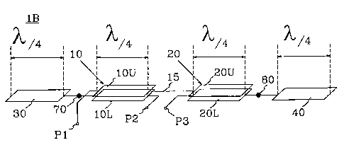
The present invention relates to a balun circuit (1B) comprising a first sub-
circuit (10) and a second sub-circuit (20) which each correspond to, or
essentially to, a .lambda./4-wave guide. The first sub-circuit (10) includes a
first conductor (10U), a second conductor (10L) and a dielectric layer
disposed between said first and second conductors, said conductors being
connected together capacitively and inductively. The second sub-circuit (20)
includes a first conductor (20U), a second conductor (20L) and a dielectric
layer disposed between said first and second conductors, said conductors being
connected together capacitively and inductively. A first side on the first
conductor (10U) in the first sub-circuit (10) is connected to an input port
(P1). A second side on the first conductor (10U) in the first sub-circuit (10)
is connected to a first side on the first conductor (20U) in the second sub-
circuit (20) via a connecting conductor (15). A second side on the second
conductor (10L) in the first sub-circuit (10) is connected to a first output
port (P2). A first side on the second conductor (20L) in the second sub-
circuit (20) is connected to a second output port (P3). A first open
terminating .lambda./4-wave guide (30) is connected to a second side on the
second conductor (10L) in the first sub-circuit (10), and a second open
terminating .lambda./4-wave guide (40) is connected to a second side of the
second conductor (20L) in the second sub-circuit (20).
La présente invention concerne un circuit balun (1B) comportant un premier sous-circuit (10) et un second sous-circuit (20) chacun correspondant au moins sensiblement à un guide d'onde .lambda./4. Le premier sous-circuit (10) comprend un premier conducteur (10U), un second conducteur (10L) et une couche diélectrique disposée entre les premier et second conducteurs, ces conducteurs étant connectés l'un à l'autre de manière capacitive et inductive. Le second sous-circuit (20) comprend un premier conducteur (20U), un second conducteur (20L) et une couche diélectrique disposée entre les premier et second conducteurs, ces conducteurs étant connectés l'un à l'autre de manière capacitive et inductive. Un premier côté du premier conducteur (10U) situé dans le premier sous-circuit (10) est connecté à un port d'entrée (P1). Un second côté du premier conducteur (10U) situé dans le premier sous-circuit (10) est connecté à un premier côté du premier conducteur (20U) situé dans le second sous-circuit (20) au moyen d'un conducteur de connexion (15). Un second côté du second conducteur (10L) situé dans le premier sous-circuit (10) est connecté à un premier port de sortie (P2). Un premier côté du second conducteur (20L) situé dans le second sous-circuit (20) est connecté à un second port de sortie (P3). Une premier raccordement de guide d'onde .lambda./4 ouvert (30) est connecté à un second côté du second conducteur (10L) situé dans le premier sous-circuit (10), et un second raccordement de guide d'onde .lambda./4 (40) ouvert est connecté à un second côté du second conducteur (20L) situé dans le second sous-circuit (20).
Note: Claims are shown in the official language in which they were submitted.
Note: Descriptions are shown in the official language in which they were submitted.
2024-08-01:As part of the Next Generation Patents (NGP) transition, the Canadian Patents Database (CPD) now contains a more detailed Event History, which replicates the Event Log of our new back-office solution.
Please note that "Inactive:" events refers to events no longer in use in our new back-office solution.
For a clearer understanding of the status of the application/patent presented on this page, the site Disclaimer , as well as the definitions for Patent , Event History , Maintenance Fee and Payment History should be consulted.
| Description | Date |
|---|---|
| Time Limit for Reversal Expired | 2009-06-26 |
| Application Not Reinstated by Deadline | 2009-06-26 |
| Inactive: Abandoned - No reply to s.29 Rules requisition | 2008-11-06 |
| Inactive: Abandoned - No reply to s.30(2) Rules requisition | 2008-11-06 |
| Deemed Abandoned - Failure to Respond to Maintenance Fee Notice | 2008-06-26 |
| Inactive: S.30(2) Rules - Examiner requisition | 2008-05-06 |
| Inactive: S.29 Rules - Examiner requisition | 2008-05-06 |
| Letter Sent | 2004-06-21 |
| Amendment Received - Voluntary Amendment | 2004-03-12 |
| Letter Sent | 2004-01-05 |
| Request for Examination Requirements Determined Compliant | 2003-12-18 |
| Request for Examination Received | 2003-12-18 |
| All Requirements for Examination Determined Compliant | 2003-12-18 |
| Letter Sent | 2002-11-26 |
| Inactive: Single transfer | 2002-10-09 |
| Inactive: Cover page published | 2002-06-26 |
| Inactive: Courtesy letter - Evidence | 2002-06-25 |
| Inactive: Notice - National entry - No RFE | 2002-06-19 |
| Application Received - PCT | 2002-04-25 |
| National Entry Requirements Determined Compliant | 2001-12-28 |
| Application Published (Open to Public Inspection) | 2001-01-04 |
| Abandonment Date | Reason | Reinstatement Date |
|---|---|---|
| 2008-06-26 |
The last payment was received on 2007-05-24
Note : If the full payment has not been received on or before the date indicated, a further fee may be required which may be one of the following
Please refer to the CIPO Patent Fees web page to see all current fee amounts.
| Fee Type | Anniversary Year | Due Date | Paid Date |
|---|---|---|---|
| Basic national fee - standard | 2001-12-28 | ||
| MF (application, 2nd anniv.) - standard | 02 | 2002-06-26 | 2001-12-28 |
| Registration of a document | 2002-10-09 | ||
| MF (application, 3rd anniv.) - standard | 03 | 2003-06-26 | 2003-06-17 |
| Request for examination - standard | 2003-12-18 | ||
| Registration of a document | 2004-05-19 | ||
| MF (application, 4th anniv.) - standard | 04 | 2004-06-28 | 2004-06-08 |
| MF (application, 5th anniv.) - standard | 05 | 2005-06-27 | 2005-06-14 |
| MF (application, 6th anniv.) - standard | 06 | 2006-06-26 | 2006-06-05 |
| MF (application, 7th anniv.) - standard | 07 | 2007-06-26 | 2007-05-24 |
Note: Records showing the ownership history in alphabetical order.
| Current Owners on Record |
|---|
| INFINEON TECHNOLOGIES AG |
| Past Owners on Record |
|---|
| DAVID WESTBERG |

