Note: Descriptions are shown in the official language in which they were submitted.
CA 02378303 2002-O1-03
1
SAW FILTER OF THE REACTANCE FILTER TYPE WITH IMPROVED
STOP BAND SUPPRESSION AND METHOD FOR OPTIMIZING THE STOP
BAND SUPPRESSION
The present invention is directed to a surface-active wave filter (SAW)
and, specifically, to a SAW filter of the reactance filter type with improved
stop band
suppression as well as to a method for the optimization of the stop band
suppression.
Reactance filters are known from classical filter technology. When SAW
resonators are employed for the individual resonators instead of discrete
elements
(inductances and capacitors), then this is called a SAW filter according to
the
reactance filter type.
Given SAW filters of the reactance filter type, SAW resonators are
employed as impedance elements. Figure 1 shows the schematic structure of a
known
resonator. It comprises metallic structures on the surface of a piezo-electric
substrate
and has a terminal pair 1-1 and 1-2 to which an interdigital transducer 1-4 is
connected for the transformation of electrical energy into acoustic energy. A
reflectorl-3 and 1-5 is respectively arranged at both sides of the
interdigital transducer
1-4 along the acoustic axis in order to prevent the acoustic energy from
escaping.
At the left, Figure 2 shows the equivalent circuit diagram for a SAW
resonator R and shows the symbol employed for the resonator at the right. A
series
2 0 resonant circuit composed of dynamic inductance L,, dynamic capacitor C,
and
dynamic resistor R, (when taking losses into consideration) is located in the
first
branch of the parallel circuit, and the static capacitor Co of the
interdigital transducer
is located in the second branch. The series resonant circuit reflects the
behavior of the
resonator in the resonance case, i.e. in the range of the resonant frequency
f~ . The
2 5 , static capacitor reflects the behavior in the frequency ranges f«f~ and
~>fr. The
dynamic capacitor C, is proportional to the static capacitor Co of the
interdigital
transducer:
(1.1)
Ci ~Co
A resonator has a resonant frequency f~ and an anti-resonant frequency fa. The
3 o following applies to the resonant frequency f,:
CA 02378303 2002-O1-03
2
f~ ' I2~ L~* C~ (1.2)
The following applies for the anti-resonant frequency fa of a resonator:
= f~* 1+ CI C (1.3)
0
The basic unit of a SAW reactance filter is what is referred to as a basic
element as shown in Figure 3. It is composed of a first resonator R, with
resonant
frequency f~, and appertaining anti-resonant frequency faP in the parallel
branch and of
a second resonator RZ with resonant frequency ~ and appertaining anti-resonant
frequency f~ in the serial branch. The frequency curve of the admittance Yp of
the
resonator R, in the parallel branch and the frequency curve of the impedance
ZS of the
resonator RZ in the serial branch are shown in Figure 4. For producing a band-
pass
filter with the middle frequency fo, the resonant frequencies of the two
resonators have
the following relationship:
faP=frs~ fo ( 1.4)
Each basic element is to be fundamentally viewed as two-port with the
terminals 3-1 or, respectively, 3-2 of port 1 and the terminals 3-3 or,
respectively, 3-4
of port 2 (see Figure 3). At the same time, the terminals 3-1 is the input and
the
terminal 3-3 is the output of the series resonator. The input of the parallel
resonator is
connected to the terminal 3-1. The terminals 3-2 and 3-4 represent the
reference
ground given an asymmetrical operation. The output 3-5 of the parallel
resonator that
2 0 faces toward the reference ground is referred to below as output side or,
respectively,
ground side of the parallel resonator. The inductance LSe~ that lies between
the output
side of the parallel resonator and the reference ground reflects the
connection to the
housing ground in the real structure.
The selection level of the SAW filter according to the reactance filter type
2 5 is defined, first, by the relationship C~/Cos of static capacitor C~, in
the parallel branch
and static capacitor Cog in the series branch and is defined, second by the
plurality of
basic elements connected following one another (cascaded).
CA 02378303 2002-O1-03
The basic elements in the case of a cascading are usually circuited
adapted, i.e. respectively mirrored. Figure 5 and Figure 6 show two examples
of a
reactance filter wherein respectively two basic elements are cascaded. The
output
impedance 5-1 (Zou~) or, respectively, 6-1 (Z;~) of the first basic element is
equal to the
input impedance 5-2 or, respectively, 6-2 of the second basic element, as a
result
whereof the losses due to mismatching are minimal. Many structures are
possible or
known for reactance filters with respect to the plurality and arrangement of
the basic
elements.
Resonators of the same type (series resonator or parallel resonator) lying
immediately behind one another can also be respectively combined to form one,
whereby the capacitative overall effect remains the same. The interconnection
of a
filter according to Figure 7 corresponds in effect to that of a filter
according to Figure
8.
Figures 9 and 10 show the typical, actual structure of a SAW filter on a
piezoelectric substrate 9-1 in a ceramic housing 9-0 and the typical
connecting
technique with bond wires 9-8 through 9-12 or, respectively, 10-9.
At the output side 9-15 through 9-17, the parallel resonators R1, R3 and
RS are connected to the housing ground pads 9-4, 9-5 and 9-7 via bond wires 9-
9, 9-
10 and 9-12.
2 0 As a result of the typical structuring technique (see Figure 9 and Figure
10), series inductances between, for example, the output side 9-17 of the
parallel
resonator RS on the substrate (chip) 9-1 and the ground 10-5 adjacent at the
outer
housing pin 9-4 are obtained given the connection of the parallel branches to
ground.
These essentially include the inductive part of the stripline on the chip, the
inductance
2 5 of the bond connection 9-9 and that of the housing lead-through 10-3.
These series inductances influence the behavior of the filter both in the
passband as well as in the stop band. f«fo applies for the pass band. The
resonant
frequency and, thus, the bandwidth of a resonator can, as known, be modified
by an
external wiring belonging to the resonator. An inductance serially with the
resonator
3 o increases the effective dynamic inductance, as a result whereof the
resonant frequency
f~ drops. Since the anti-resonant frequency fa is shifted to only a very
slight extent, the
CA 02378303 2002-O1-03
4
bandwidth ~~fa fr of a resonator is increased with the serial inductance. The
bandwidth of the SAW filter is also increased in the case of a parallel
resonator.
f«fo and ~>fo applies for the stop band. Here, the equivalent circuit
diagram of a resonator is reduced to its static capacitance Co since the
series resonant
circuit is extremely high-impedance beyond fo and corresponds to a no-load. An
inductance Lse~ serially with the resonator yields a series resonant circuit
shown in
Figure 11 having a resonant frequency
~~ = 1/27L Lser * CO (1.5)
In the case of an inductance serially with a parallel resonator, this means
that the energy of the filter can flow off directly to ground given the
frequency f~,;
what is referred to as a pole point thus forms in the filter curve, i.e. an
increased
suppression in the stop band. A plurality of pole points in the stop band
corresponds
to the plurality of parallel branches with series inductance. Pole points f~"
and fPo,z
that can be distinguished from one another in terms of frequency derive only
given
different products II,=Lsen*Co, arid IIz=Lserz*Cor When the products are
identical,
then the pole points lie at the same frequency; a double pole point fpo, =
fpo" =f~o~z is
obtained with a higher suppression than given a simple pole point.
Figure 11 a shows the attenuation behavior of a resonator in the parallel
branch to which an inductance Lser is serially connected at.the output side of
the
2 o parallel resonator. As in Figure 1 1b, the series resonant circuit of the
resonator whose
resonant frequency f,~ = fo was removed in order to illustrate the pole point.
What
typically"applies for the frequency of the pole point fpo, is fpa, > fo,
whereby fo is equal
to the resonant frequency of the filter. A high attenuation is then obtained
for the
pole point.
2 5 SAW filters of the reactance filter type are mainly employed as RF filters
in the mobile radio telephone field since they exhibit extremely low losses in
the pass
band. As RF filter in the mobile radio telephone field, the SAW filter of the
reactance
filter type must, over and above this, suppress, first, the duplex band (i.e.,
the
reception band given a transmission filter and, conversely, the transmission
band
3 o given a reception filter) and, second, must suppress the signal at the
local oscillator
CA 02378303 2002-O1-03
frequency (LO) and/or at the image frequency in order to prevent unwanted
mixed
products in the telephone.
The local oscillator lies above or below the middle frequencies fo of the
filter. The distance from the middle frequency fo corresponds to the
intermediate
5 frequency (ZF) employed for the signal editing. The image frequency has the
spacing
2*ZF from the middle frequency fo. Since momentary ZF frequencies in the range
100-400 MHz are employed, the SAW filter - dependent on the application - must
comprise good attenuation properties of, typically, more than 30 dB in the
range fo
plus/minus 100-800 MHz. In the most frequent instances, the local oscillator
lies
above the middle frequency fo.
There are various possibilities for achieving an adequate attenuation in the
range of the LO frequency and/or image frequency. Possibly A is comprised
therein
that the general selection level be made correspondingly high (the minimum
attenuation below the pass band given approximately f~/2 is valid as criterion
for this).
The great disadvantage is, however, that the losses in the pass band also
increase with
increasing selection level. This is unacceptable for the signal processing in
the
telephone in most cases. The second possibility B derives from the
aforementioned
fact that an inductance present given the traditional structuring technique
generates a
pole point serially with a parallel resonator that lies exactly at the LO or
image
2 0 frequency. Given the great spectrum of ZF frequencies employed, a
possibility must
be established in this case in order to vary the generated pole point over a
range of
approximately 700 MHz.
Since the static capacitance C~, in the parallel branch is the determining
factor for the filter performance (passband, matching and selection level), it
can only
2 5 be varied to an extremely slight degree with given filter demands such
that the
position of pole points in the stop band also simultaneously changes.
Likewise, the
degree of freedom for the size of the inductance serially between output side
of the
parallel resonator and ground is limited. Due to the necessity for
miniaturization as
well as for cost reasons, the chips that are employed are becoming smaller and
3 o smaller, this resulting therein that the inductive part of the stripline
on the chip can be
varied to only a limited extent. The length and the inductance of the bond
connection
CA 02378303 2002-O1-03
6
correlating therewith can likewise hardly be varied any more with any housing
in the
course of the progressing miniaturization. Moreover, the inductance that
derives from
the housing lead-through is fixed for a given housing.
The possibility B is thus also not established anymore to an adequate
extent for SAW filters according to the reactance filter type in housings that
have
been miniaturized further, namely it is no longer established to an adequate
degree in
order to assure the LO and/or image suppression by means of suitably placed
pole
points over a great frequency range from fo plus 100-800 MHz. Particularly
given the
future connection technology of "flip-chip-technique" wherein bump connections
are
1 o employed instead of the bond wires, it is impossible to generate pole
points at
relatively low frequencies, i.e. in the range of 100 MHz above the middle
frequency
fo, since the inductances present given this structuring technique serially to
the output
side of a parallel resonator are too small (see Equation 1.5), and the static
capacitances of the parallel branches can likewise not be selected great
enough
because of the required self matching to SOS2.
It is therefore an object of the present invention to specify a way of how a
filter can be designed such that an improved stop band suppression can be
obtained
for specific LO frequencies and image frequencies over a possible range from
100
through 800 MHz next to the middle frequency. In particular, a way should be
2 0 specified for shifting pole points of a reactance filter into a desired
region close to the
middle frequency fo without greatly influencing the remaining filter behavior.
This object is inventively achieved with a filter according to claim 1.
Advantageous developments in a method for shifting pole points may be derived
from
further claims.
2 5 As a result of a connection of the ground-side output sides of the
parallel
branches respectively comprising a resonator on the chip, a coupling of the
parallel
branches is inventively produced, as a result whereof the frequency position
of the
appertaining pole point (also referred to as "coupled pole point" below) can
be
modified to a great extent. As a result thereof, it is possible to produce a
SAW filter
3 o that comprises pole points at lower frequencies than could be achieved by
the
previous, serial interconnection of the parallel branches with existing,
structure-
CA 02378303 2002-O1-03
7
conditioned inductances according to Equation (1.5). It is also possible to
shift one or
more pole points in a given filter over a broader frequency range than was
hitherto
possible in a given filter. With the invention, thus, a pole point can be
generated
exactly at the frequency at which a high selection is required, for example at
an
arbitrary LO or image frequency.
Such demands for the suppression of signals at the local oscillator
frequency (LO suppression) and/or at the image frequency (image suppression)
can
thus still be satisfied in extremely small housings having very low structure-
conditioned inductances. One or more pole points can be shifted to a desired
frequency given an established bond inductance, conduct inductance or housing
lead
through inductance without this requiring an increase in the serial
inductance.
Additionally, of course, the serial inductance can also be increased.
Moreover, the plurality of ground connections that are offered can be set
independently of the plurality of parallel branches employed, this leading to
a lower
space requirement. It is precisely in view of new connecting technologies
(bump
connections instead of bond connections) and new housing technologies that the
embodiments according to the invention represent the sole possibility for
achieving
the aforementioned selection demands in miniaturized housings.
The principle for shifting the pole points according to the present
2 o invention shall be explained in greater detail below on the basis of
exemplary
embodiments and the appertaining figures. The following, concrete embodiments
are
examples of the employment in a SAW filter of the reactance filter type.
Thereby shown are:
Fig. 1 a one-port SAW resonator;
2 5 Fig. 2 the equivalent circuit diagram and symbol for a SAW resonator;
Fig. 3 a basic element of a SAW filter of the reactance filter type;
Fig. 4 interaction of parallel and series resonators;
Fig. 5 cascade of two basic elements;
Fig. 6 cascade of two basic elements;
3 0 Fig. 7 diagram of a reactance filter;
Fig. 8 diagram of a reactance filter with the reduced structure s-p-s-p;
CA 02378303 2002-O1-03
8
Fig. 9 plan view onto a SAW filter in the housing without
cover;
Fig. 10 cross-section through a SAW filter in the housing;
Fig. 11 pole point;
a
Fig. 1 1b equivalent circuit diagram for the attenuation
behavior of a parallel
branch;
Fig. 12 equivalent circuit diagram of a filter;
Fig. 13 equivalent circuit diagram for the attenuation
behavior of a SAW filter;
Fig. 14 diagram that shows the relationship between 0
L~~ and pole point;
Fig. 15 dependency of the frequency position of the pole
point on the static
capacitance;
Fig. 16 filter having three basic elements;
Fig. 17 the equivalent circuit diagram thereof in the
stop band;
Fig. 18 the attenuation behavior thereof;
Fig. 19 filter with four basic elements;
Fig: the equivalent circuit diagram thereof in the
stop band;
Fig. 21 the attenuation behavior thereof;
Fig. 22 filter with four basic elements;
Fig. 23 the equivalent circuit diagram thereof in the
stop band;
Fig. 24 the attenuation behavior thereof;
2 0 Fig. filter with four basic elements;
Fig. 26 the equivalent circuit diagram thereof in the
stop band;
Fig. 27 the filter characteristic thereof;
Fig. 28 filter with four basic elements
Fig. 29 the equivalent circuit diagram thereof in the
stop band;
2 5 Fig. filter structure with bump connection;
Fig. 31 filter structure with bond connection.
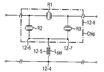
Fig. 12 shows a simple filter structure of the
invention symbolically as a
equivalent
circuit
diagram,
this being
potentially
part of
a larger
filter
structure
with
further
basic elements.
Given (at
least)
two of
the parallel
branches
with the
parallel
3 0 resonatorsR2 and R3, the output sides 12-6 and 12-7 are
already inventively
electrically
connected
to one
another
on the
chip (substrate)
12-8. Only
thereafter
CA 02378303 2002-O1-03
9
does a connection to the housing ground pad 12-4 comprising, for example a
bond
connection 12-5, ensue.
Fig. 13 shows the equivalent circuit diagram for the frequency range f«fo
and f5>fo wherein only the static capacitance Co takes effect for each
resonator. The
selection behavior of a SAW filter according to the reactance filter type can
be largely
described with this reduced equivalent circuit diagram. The inductance Lser
corresponds to the inductance between the connection of the parallel
resonators on the
chip and the housing ground pin (equals terminal for ground at the housing)
outside.
A coupling of the two parallel branches already electrically connected on
1 o the chip occurs. This leads to a frequency position change of the pole
points in the
stop band. The frequency position of the coupled pole point can be identified
on the
basis of the equivalent circuit diagram from Figure 13, which shows a two port
Z.
The two port Z then comprises a pole point when the impedance to ground
becomes
zero.
Zz l = 0
Zzl is thereby a systematically referenced matrix element from the impedance
matrix.
For determining Zzl, the two port Z can be divided into a series circuit of
the two-
ports Z' and Z". The two-port Z' comprises the II-circuit composed of the
three
capacitors Copl, Copz and Cps. The two-port Z" comprises only the inductance
Lser. The
2 0 following thus derives:
I
,1-
COpI COp2 (2.1
C Os
Z21 .~~ Lser 2.2)
Whereby j= represents the imaginary number and c~ = 2n f applies.
With
2 5 Zzl = Z'zi + Z"z, (2.3)
CA 02378303 2002-O1-03
1~
it follows that
I-~ZLI~. Cope + Copl + CoC op~)
Z21 _ or (2.4)
,JCV Cop, + Copi + Cop~Cop~
COI
When the numerator of the expression of (2.4) becomes zero,
1 CVZLssrCCOp2 -~ C~p~ -+- CoC Op3~ _
01
Zz, becomes zero. The following is obtained therefrom for the frequency
position of
the coupled pole point:
1
f Dol (coupled) - ~ ( 2 . 6 )
~ "OplCOpl
211 Lssr "Op? + C0p1 +
COs
It can be clearly seen compared to the pole points previously obtained
without coupling of the parallel branches on the chip according to Equation
(1.5).
1-ser * CoP~ (2.7)
fpol2 12~ User * Copt (2.8)
CoPICoP2
That the additional capacitance parts and Copt or, respectively,
C os
1 o Cop, shift the coupled pole point to a far lower frequency given the same
inductance
User
Numerical example: for a known SAW filter of the reactance filter type,
the frequency fpo, of a pole point is calculated as:
CA 02378303 2002-O1-03
11
fPo~ 1 - 12~ ~ser'Copl - 12~ nH' 4pF = 2.52 GHz
Typical values of 1nH and 4pF were thereby assumed for the serial inductance
Lse,
and for the static capacitance CoP.
According to Equation 2.6 and given the same assumed values for Lser and
C~ and likewise given 4pF for Cos,
fPo, 2 = 12n 1nH* (rpF + 4pF + (4pF) Z l 4pF) = 1.45 GHz
derives when two parallel branches are coupled.
When a filter comprises a plurality of parallel branches, then a plurality of
parallel branches can also be connected to one another at the ground side,
these also
continuing to be referred to as "coupled parallel branches". The plurality and
combination of the connected parallel branches plays a critical part for the
frequency
position of the coupled pole points and is to be taken into consideration in
the
selection of the filter structure for a desired frequency position of the pole
points.
Fig. 14 indicates the dependency of the position of a coupled pole point on
the size of the inductance Lser. The two curves 14-1 and 14-2 indicate the
filter
behavior for the same filter, whereby only Lse~ has been differently selected.
A
different frequency position of the pole points derives dependent on Lse~,
whereby the
inductance Lser 1 belonging to f~, 1 is smaller than L~~ 2. The shift of the
pole points
toward lower frequencies is all the greater the higher the inductance Lser is.
2 0 To a lesser extent, the frequency position of the pole point can be set by
a
variation of the product of static capacitances of the coupled parallel
branches
IIpC = C~, * C~z (2.9)
So that the filter behavior in the passband and the general selection level is
not
modified, such a variation of the product of static capacitances in the
parallel branch
2 5 can be implemented only upon retention of their sum:
E CP = C~, + C~,2 = constant (2.10)
CA 02378303 2002-O1-03
12
The following method can be applied: the static capacitance Cop, of the
first couple parallel resonator is increased by the same amount C~o~s~
C~,(new) = CoP, + C~o~s~ (2.11)
by which the static capacitance C~z of the second couple parallel resonator is
lowered:
CoP2(new) = C~,z - C~o~S~ with C~o~s, ~ C~2, (2.12)
so that the product E CP in fact changes but the sum of the static
capacitances remains
identical.
E Cp = C~,(new) + C~Z(new) = C~,, + C~z = constant (2.13)
and no modifications of the passband or of the general selection level need be
accepted.
When a greater frequency offset of the couple pole point is necessary, the
participating static capacitances C~,,, C~2 or CoS can be varied. When more
parallel
resonators than the two parallel resonators to be coupled are present, then
the sum C~,
+ C~,2 can be raised (or lowered), and the static capacitance of a non-coupled
parallel
resonator can be lowered-(or raised) for balancing such that the total sum of
all static
capacitances remains the same in the parallel branches. The general selection
level is
retained as a result thereof.
Fig. 15 shows how, given a constant inductance Lser, the frequency of the
couple pole point is increased as a result of a reduction of the sum of the
static
2 o capacitances C~,+ C~z of the coupled parallel branches, being increased by
the factor
1.2. For balancing, the static capacitance of a further parallel branch was
correspondingly increased.
Another possibility for shifting the couple pole point is comprised in
intentionally splitting a parallel resonator P into two individual resonators
P' and P"
2 5 parallel to one another, whereby the sum of the capacitances of the split,
individual
resonators is equal to the original capacitances C~:
C~, = C,~+ C" ~.
When one of these parallel resonators P' is coupled with a further parallel
resonator but not with the parallel resonator P", then the frequency position
of the
CA 02378303 2002-O1-03
13
coupled pole point can be set on the base is of the division ratio CeP of the
static
CeP
capacitance of the split parallel resonators P' and P", since C'~, influences
the
frequency position of the coupled pole point.
A single series resonator or a plurality of series resonators can be arranged
between coupled parallel branches. Since the size of the static capacitance
Cos that
lies between the coupled parallel resonators influences the frequency position
of the
coupled pole point according to Equation 2.6, the frequency position of the
coupled
pole point can likewise be shifted with the following method.
When further series resonators S~ in addition to the series resonator or
resonators S lying between the coupled parallel branches are present, then the
static
capacitance Cos thereof can be raised (or lowered) and, for balancing, the
static
capacitance of the series resonators S~ that do not lie between the coupled
parallel
resonators can be lowered (or raised) such that the total sum of all static
capacitances
in the series branches remains the same. As a result thereof, the general
selection
level is retained and the frequency position of the coupled pole point is
modified.
As already explained, the range for the variation of the static capacitances
Cp in the parallel branch and of the serial inductances L~~ (between the
connection of
the parallel branch on the chip and the outside terminal at the housing) is
limited. The
same is therefore also true for the frequency range in which the pole points
can be
2 o displaced. In contrast to the measures known from the prior art, however,
the range of
variation achieved according to the invention enables the manufacture of SAW
filters
- even given extremely miniaturized housings - with a LO suppression and image
suppression that is required for the employment as IZF filter in the mobile
radio
telephone field.
2 5 Concrete embodiments of inventive filters are now recited below.
Embodiment 1 (also see Fig. 16 through Fig. 18):
CA 02378303 2002-O1-03
14
A structure having three basic elements is employed. A first basic element
is connected such to the input port 16-1 that both the parallel branch as well
as the
series branch comprise a connection to the input port. The second basic
element is
connected according to the matching demand Zo~~ = Z;~. The third basic element
follows in the same way. Differing from the case at the input port, only one
series
branch is thus directly connected to the output port. A sequence p-s - s p - p-
s for the
resonators derives from the input to the output, wherebyp stands for parallel
resonator
and s stands for series resonator. Fundamentally, input port and output port
can be
interchanged without modifying the filter properties, whereby the sequence s p
p-s-s-
1 o p derives.
As known, identical resonators can also be combined upon retention of
their capacitative effect. The following structures with minimum number of
resonators thus derive:
p-s p-s or, respectively, s p-s p
however, mixed forms having partial combination of the resonators area also
possible:
p-s p p-s or, respectively, s p p-s p
p-s-s p-s or, respectively, s p-s-s p
For the sake of simplicity, the embodiments below are only explained on
the basis of minimum of resonators and without additional indication of the
2 0 interchangeability of input port and output port and are shown this way in
the Figures.
Nonetheless, the invention also comprises modifications according to the
example
that has just been explained above.
Fig. 16 symbolically shows the structure of embodiment 1. The two
parallel branches are already electrically connected to one another on the
chip and a
2 5 connection to the housing only ensues subsequently. The equivalent circuit
diagram
for the selection behavior in the range f«fo and f>>fo is shown in Fig. 17.
The
inductance LS~~ corresponds to an inductance between the connection of the
parallel
resonators on the chip and the housing ground pin outside.
The filter has a filter characteristic as identified by curve 18-1 in Fig. 18.
3 o The comparison to filter curve 18-2 (corresponding to the filter shown in
Fig. 8)
wherein the parallel branches on the chip are not connected to one another,
clearly
CA 02378303 2002-O1-03
shows how the frequency position of the pole points in the stop band with a
typical
inductance Leer = 1.0 nH is shifted by the connection of the parallel branches
on the
chip. The selection is increased by more than 10 dB in the frequency range
between
the vertical lines (typical frequency range for LO suppression and image
suppression
5 given low intermediate frequency).
Embodiment 2 (also see Fig. 19 - Fig. 21):
Fig. 19 symbolically shows the structure of a second inventive
embodiment wherein a structure having four basic elements is employed. A first
basic element is connected such to the input port 19-1 that both the parallel
branch as
10 well as the series branch comprise a connection to the input port. The
second basic
element is connected according to the matching requirement Zo"~ = Z;". Basic
element
3 and 4 follow in the same way. Just as at the input port, both a parallel
branch as
well as a series branch are thus directly connected to the output port 19-3. A
sequence
for the resonators from the input to the output derives as follows:
15 p-s p-s p
whereby p stands for parallel resonator and s stands for series resonator.
Resonators of
the same type are already combined.
Two of the three parallel branches are already electrically connected to
one another on the chip and a connection to the housing only ensues
subsequently via
2 0 the inductance L~~z. The remaining parallel branch is connected to the
housing
independently thereof via the inductance Lsern The equivalent circuit diagram
for the
selection behavior in the range f«fo and f5>fa is shown in Fig. 20. The
inductance
Lserz corresponds to an inductance between the connection 19-4 of the parallel
resonators on the chip (shown with the broken line in the Fig.) and the
housing
2 5 ground pin outside.
In Fig. 21, the curve 21-1 shows the filter characteristic of the filter from
Fig. 19. The comparison with the filter curve 21-2 wherein the parallel
branches are
not connected on the chip clearly shows how the frequency position of the pole
points
in the stop band given a typical inductance Lserz = 1.OnH is shifted toward
lower
3 o frequencies due to the connection of two of the three parallel branches on
the chip
CA 02378303 2002-O1-03
16
here. The selection is increased by approximately 10 dB in the frequency range
between the vertical lines (typical frequency range for LO suppression and
image
suppression at low intermediate frequency).
Embodiment 3 (also see Fig. 22 - Fig. 24):
Fig. 22 symbolically shows the structure of the inventive embodiment 3.
A structure having three basic elements is employed. A first basic element is
connected such to the input port 22-1 that only the series branch comprises a
connection to the input port. The second basic element is connected according
to the
matching requirement Zo~, = Z;". Basic element 3 and 4 follow in the same way.
Just
as at the input port, only one series branch is thus directly connected to the
output port
22-3. A sequence for the resonators from the input to the output derives as
follows:
s p-s p-s
whereby p stands for parallel resonator s stands for series resonator.
Resonators of the
same type are already combined. The two parallel branches are already
electrically
connected to one another on the chip and a connection to the housing only
ensues
subsequently. The equivalent circuit diagram far the selection behavior in the
range
f«fo and ~>fo is shown in Fig. 23. The inductance Lser corresponds to an
inductance
between the connection of the parallel resonators on the chip and the housing
ground
pin outside. The filter from 22 has a filter characteristic as identified by
curve 24-1 in
2 0 Fig. 24. The comparison to the filter curve 24-2, whereby the parallel
branches are
not connected on the chip, it clearly shows how the frequency position of the
pole
points in the stop band given a typical inductance L~~ = 1.0 nH is shifted due
to the
connection of the two parallel branches on the chip. The selection is
increased by
more than 8 dB in the frequency range between the vertical lines (typical
frequency
2 5 , range for LO suppression and image suppression at high intermediate
frequency).
Embodiment 4 (also see Fig. 25 - Fig. 2~:
Fig. 25 symbolically shows the structure of the inventive embodiment 4.
A structure and four basic elements is employed. A first basic element is
connected
such to the input port 25-1 that only the series branch having the resonator
RS,
CA 02378303 2002-O1-03
17
comprises a connection to the input port. The second basic element is
connected
mirrored because of the matching demand Zo"~ = Z.". Basic element 3 and 4
follow in
the same way. Just as at the input port, only one series branch is thus
directly
connected to the output port 25-3. A sequence for the resonators from input to
output
derives as follows:
s p-s p-s
Resonators of the same type are already combined; in contrast to the
embodiment 3, however, one parallel branch has been intentionally divided
again. The
division ensues such that each parallel resonator Rpz, Rp3 foams its own two-
port with
1 o its own electrical inputs and outputs. The combined parallel branch having
the
resonator Rp, together with one of the non-combined, two parallel branches
(Rpz) are
already electrically connected to one another on the chip at .25-2, and a
connection to
the housing only ensues subsequently via LseTn The remaining parallel branch
(Rp3) is
connected to the housing independently thereof. The equivalent circuit diagram
for
the selection behavior in the range f«fo and f5>fo is shown in Figure 26. The
inductance Lser~ corresponds to an inductance between the connection of the
parallel
resonators Rp, and Rpz on the chip and the housing ground pin outside; the
inductance
Lse~z corresponds to an inductance between the parallel resonator RP3 on the
chip and
the housing ground pin outside.
2 o The filter from Fig. 25 has a filter characteristic that is characterized
by
curve 27-1 in Fig. 27. The comparison to the filter curve 27-2, wherein the
output
sides of the parallel branches are not connected on the chip, clearly shows
how the
frequency position of the pole points in the stop band given a typical
inductance Lsesn
= 1.0 nH is shifted due to the connection of two of the three parallel
branches on the
2 5 chip. The selection is increased generally by more than 5 dB in the
frequency range
between the vertical lines (typical frequency range for LO suppression and
image
suppression given high intermediate frequency). The selection gain is far more
than
10 dB when either a high LO suppression or image suppression is demanded.
Embodiment 5 (also see Fig. 28-Fig. 30):
CA 02378303 2002-O1-03
18
Fig. 28 symbolically shows the structure of the inventive embodiment S.
A structure having four basic elements is employed. A first basic element is
connected such to the input port 28-1 that only the series branch comprises a
connection to the input port. The second basic element is connected according
to the
matching demand Zo~~ = Z;~. Basic element 3 and 4 following in the same way.
Just
as at the input port, only one series branch is thus directly connected to the
output port
28-3. A sequence for the resonators from input to output derives as follows:
s p-s p p-s
Resonators of the same type are already combined similar to embodiment
4; however, one parallel branch is intentionally divided again. The division,
however,
does not ensue into two parallel resonators that are independent of one
another but in
the form of a three-port. The input 4 both parallel resonators is composed of
a shared
terminal strip 28-4 at which the interdigital fingers to be excited lie. The
terminal
strip of the output is divided into two bus bars 28-5 and 28-6, whereby each
bus bar
corresponds to the output of one of the two parallel resonators.
The parallel branch with the resonator Rp, together with one of the non-
combined parallel resonators Rp2 are already electrically connected to one
another on
the chip at the ground output 28-2. A connection to the housing only ensues
subsequently. The remaining parallel branch with the parallel resonator Rp3 is
2 o connected to the housing independently thereof. The equivalent circuit
diagram for
the selection behavior in the range f«fo and ~>fo is shown in Fig. 29. It is
basically
comparable to the equivalent circuit diagram in Fig. 26. The inductance Lsea
corresponds to an inductance between the connection of the parallel resonators
Rp,
and Rpz on the chip and the housing ground pin outside; the inductance LSer2
2 5 corresponds to a further inductance between the non-coupled resonator Rp3
and the
housing ground pin outside.
The filter from Fig. 28 has a filter characteristic that does not differ from
the filter from Fig. 26 and is therefore also characterized by curve 27-1 in
Fig. 27. In
contrast to the embodiment 4, a different form of the division of a parallel
resonator is
3 0 shown here, this differing essentially in the layout but not in the effect
on the selection
behavior.
CA 02378303 2002-O1-03
19
Fig. 31 shows portions of an inventive filter structure as a schematic plan
view onto a substrate. The resonators R are shown as interdigital transducers.
The
two coupled resonators Rp, and Rp2 in the parallel branch are electrically
connected to
one another on the substrate and comprise a shared ground connection 31-1 that
is
connected to a ground terminal pad 31-3 by a bond wire 31-2, which represents
one
part of the inductance Lse~. The connection on the substrate is realized here
with a
stripline but can also comprise a bond wire. Even though only two coupled
resonators
are shown here, the invention also covers filters having more than two coupled
resonators.
CA 02378303 2002-O1-03
Embodiment 6:
The description of a sixth embodiment of the present invention now
follows, portions thereof being shown in Fig. 30. A SAW filter of the
reactance filter
type having at least two parallel branches is employed. In at least two of all
existing
5 parallel branches R2 and R3, the output sides (30-3 and 30-4) of the
parallel
resonators are already electrically connected to one another electrically on
the chip.
The connection 30-5 to the housing only ensues subsequently. The remaining
parallel
branches are connected to the housing independently thereof. The connection of
the
chip (30-1 ) to the housing is not implemented as previously as a bond
connection but
1 o is produced with a bump connection (30-5).
The equivalent circuit diagram for the selection behavior in the range
f«fo and f5>fo has not changed compared to the general exemplary embodiment
and
can be seen in Fig. 13. The inductance LSeT corresponds to an inductance
between the
connection of the parallel resonators on the chip and the housing ground pin
outside.
15 Given a structuring in bump technology, the value for the inductance Lser
is greatly
reduced compared to an embodiment with bond wire since the bond connection
itself
has its nearly no inductance in contrast to a bond connection. Only the
inductive part
of the stripline on the chip and the housing lead-through inductance up to the
external
housing ground pin remaining.
2 0 Fundamentally, all of the exemplary embodiments shown up to now, even
though it is with more than four basic elements having at least two parallel
branches
at the output side already electrically connected on the chip, can be realized
in
conjunction with the bump technology. The filter characteristics are also
fundamentally comparable; however, the value that can be achieved for the
serial
2 5 inductance Lser is lower. In order to achieve the required selections, for
example in
the range of the LO suppression and/or image suppression, it is thus all the
more
necessary to employ the inventive method for targeted variation of the stop
band. The
invention also offers the advantage of reducing the plurality of necessary
ground
bumps and, thus, the chip area for ground terminals. As a result thereof, the
overall
3 0 SAW filter can be miniaturized even further.