Note: Descriptions are shown in the official language in which they were submitted.
CA 02378380 2002-O1-07
WO 01/04809 PCT/US00/15357
AUTOMATED OPTICAL CHIP HOLDER FOR A PIGTAILING SYSTEM
BACKGROUND OF THE INVENTION
1. Field of the Invention
The present invention relates generally to an optical chip holder in a
pigtailing
system, and particularly to an automated optical chip holder that loads the
optical chip
and unloads the pigtailed optical chip in an automated mass-pigtailing system.
2. Technical Background
Optical fibers must be precisely and securely aligned with integrated optical
chip waveguides during a pigtailing procedure. Otherwise, light signals
propagating
through the resulting device will be severely degraded by attenuation and
other optical
losses. In addition, processes depending on the extensive use of manpower, are
undesirable. From an efficiency standpoint, it is most desirable that the
entire pigtailing
process for loading the optical chip, precision aligning, pigtailing, and
unloading be
automated and reproducible.
One approach that has been considered involves the use of vacuum chucks.
Typically, the optical chip is placed on a chuck platform surface having air
ducts which
communicate to a plenum. Subsequently, the air in the plenum is evacuated and
the
resulting vacuum force holds the optical chip against the platform surface.
However,
this approach has several drawbacks. First, vacuum chucks tend to produce air
fluctuations that induce small vibrations, perturbing the optical chip. Thus,
the stability
of the optical chip is not maintained during the curing of the glue. More
importantly,
retraction stresses during the curing of the glue cause the optical chip's
waveguides to
CA 02378380 2002-O1-07
WO 01/04809 PCT/US00/15357
2
be misaligned with the fiber or fiber array block. As a result, the device has
a lower
reliability and the resulting optical losses are high. Another drawback
associated with
this method is the dependency on skilled labor. An operator is required to
load the
optical chip and unload the pigtailed optical chip manually. Since this is a
very delicate
operation, the success of the pigtailing process is largely dependent on the
experience of
the operator.
In another approach that has been considered, a slide mechanism is used to
hold
the optical chip in place. The face of the optical chip substrate is used as a
support
reference. The slide mechanism slides against the substrate face to clamp it
against a
support. Although the stability of the optical device is improved, the
resulting chip
thickness dispersion tends to negatively affect the reproducibility of the
process. Like
the method described above, this method requires that an operator load the
optical chip
and unload the pigtailed optical chip manually. Again, since this is a very
delicate
operation and the success of the pigtailing process is dependent on the
experience of the
operator.
Thus, a need exists for an automated chip holder that precisely, securely, and
repeatedly positions and aligns optical chips within the pigtailing system.
Further, a
need exists for an automated chip holder that automatically loads the optical
chip and
unload the pigtailed optical chip with minimal operator involvement; one that
is
suitable for mass-producing pigtailed optical devices.
SUMMARY OF THE INVENTION
The present invention addresses the problems of the conventional systems
discussed above. The automated chip holder of the present invention
automatically
loads and precisely positions the optical chip at a predetermined position.
The chip is
clamped in position for pigtailing using soft resilient materials that secure
the chip in
two dimensions. The resilient clamp materials compensate for irregularities in
the hard
surfaces of the chuck platform causing the pressure that is exerted on the
chip to be
more uniformly distributed. Thus, micro-vibrations are substantially reduced
and
damage to the chip is avoided, resulting in improved manufacturing yields. In
addition,
CA 02378380 2002-O1-07
WO 01/04809 PCT/US00/15357
the resiliency of the clamp materials will compensate for relatively coarse
positional
adjustments of the chuck assembly during positioning and alignment. After
pigtailing,
the pigtailed chip is automatically unloaded with minimal operator
involvement. The
chip holder accomodates optical chips having various shapes and sizes.
One aspect of the present invention is an automated chip holder for
positioning
an optical chip in a pigtailing system. The optical chip has a registration
edge and a
registration surface. The automated chip holder positions the optical chip in
a three
dimensional space characterized by a rectangular coordinate system having an x-
axis, y-
axis, and z-axis. The automated chip holder includes: a support base having a
slide
track disposed parallel to the x-axis; a registration member fixed to the
support base for
defining an alignment position in the three dimensional space; an adjustable
chuck
assembly slidably disposed on the slide track for moving the optical device
between a
device interchange position and the alignment position, the adjustable chuck
assembly
being movable in the x-axis direction and adjustable in the z-axis direction
in response
to a force directed in the x-axis direction; and a drive unit connected to the
adjustable
chuck assembly for applying the x-axis force to said adjustable chuck
assembly.
In another aspect, the present invention includes a method for positioning an
optical device in a pigtailing system using an automated chip holder. The
optical
device includes a registration edge and a registration surface. The automated
chip
holder includes a support base having a slide track, a registration member
fixed to the
support base for defining an alignment position in a three dimensional space
characterized by a rectangular coordinate system having an x-axis, y-axis, and
z-axis.
The method for positioning comprising the steps of: providing an adjustable
chuck
assembly slidably disposed on the slide track for moving the optical device
between a
device interchange position and the alignment position, the adjustable chuck
assembly
being movable in the x-axis direction and adjustable in the z-axis direction
in response
to an x-axis force; and applying the x-axis force to thereby move the optical
device
from a device interchange position to the alignment position.
Additional features and advantages of the invention will be set forth in the
detailed description which follows, and in part will be readily apparent to
those skilled
CA 02378380 2002-O1-07
WO 01/04809 PCT/US00/15357
4
in the art from that description or recognized by practicing the invention as
described
herein, including the detailed description which follows, the claims, as well
as the
appended drawings.
It is to be understood that both the foregoing general description and the
following detailed description are merely exemplary of the invention, and are
intended
to provide an overview or framework for understanding the nature and character
of the
invention as it is claimed. The accompanying drawings are included to provide
a
further understanding of the invention, and are incorporated in and constitute
a part of
this specification. The drawings illustrate various embodiments of the
invention, and
together with the description serve to explain the principles and operation of
the
invention.
BRIEF DESCRIPTION OF THE DRAWINGS
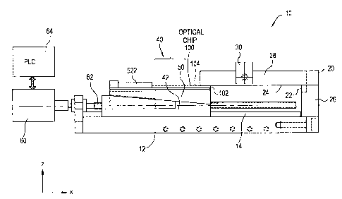
Figure 1 is a side elevation view of the automated chip holder of the present
1 S invention;
Figure 2 is a rear elevation view of the automated chip holder of the present
invention;
Figure 3 is a detail view illustrating the uniform force applied in the z-
direction
during alignment;
Figure 4 is a detail view of a registration member of the present invention;
Figure 5 is a detail view of a side elevation of an adjustable chuck assembly
of
the present invention;
Figure 6 is a detail view illustrating the uniform force applied in the x-
direction
during alignment;
Figure 7 is a detail view of a rear elevation of the adjustable chuck assembly
of
the present invention.
Figure 8 is a detail view of the device interchange position of the automated
chip holder of the present invention;
Figure 9 is a detail view of an alignment position of the automated chip
holder
of the present invention.
CA 02378380 2002-O1-07
WO 01/04809 PCT/US00/15357
DETAILED DESCRIPTION OF THE PREFERRED EMBODIMENTS
Reference will now be made in detail to the present preferred embodiment of
the invention, an example of which is illustrated in the accompanying
drawings.
Wherever possible, the same reference numbers will be used throughout the
drawings to
refer to the same or like parts. An exemplary embodiment of the automated chip
holder
of the present invention is shown in Figure l, and is designated generally
throughout by
reference numeral 10.
In accordance with the invention, the present invention for an automated chip
holder 10 includes an adjustable chuck assembly 40 which moves optical chip
100 to a
precise location in three dimensional space. Optical chip 100 is disposed on a
resilient
pad and adjacent to a resilient wedge to protect the chip from damage during
clamping.
The resilient material applies uniform clamping forces acting in a horizontal
and
vertical direction during the pigtailing process. This is an important feature
that
absorbs micro-vibrations, eliminating chip misalignment due to retraction
stresses.
There are other advantages associated with using the resilient materials. The
incremental movements of the clamp need not be as precise as a clamp having a
hard
non-resilient surface. If a non-resilient clamp exerts too much force on the
chip, it will
damage the chip. Thus, the motion control system must be implemented using
stricter
tolerances to avoid such damage. On the other hand, the resilient material is
forgiving
and accomodates a chuck assembly having coarser incremental movements when
clamping. Thus, the necessity of precision motion control is avoided along
with the
concomitant cost. Note also, that the resilient wedge is interchangeable
allowing the
adjustable chuck assembly 40 to accomodate optical chips having various sizes
and
shapes.
As discussed above, automated chip holder 10 positions optical chip 100 at a
precise location in three-dimensional space. Movement in the three dimensional
space
is described throughout in reference to a Cartesian coordinate system having
mutually
orthogonal x, y, and z axes. The length of automated chip holder 10
corresponds to an
x-axis, the width corresponds to a y-axis, and the height corresponds to a z-
axis.
CA 02378380 2002-O1-07
WO 01/04809 PCT/US00/15357
6
As embodied herein, and depicted in Figure 1, automated chip holder 10
includes a support base 12 which functions as a chassis for automated chip
holder 10.
Support base 12 includes slide track 14, which is a raised portion used for
guiding
adjustable chuck assembly 40 in either direction along the x-axis.
Registration member
20 is connected to support base 12 and defines the alignment position of
optical chip
100 in three-dimensional space. Adjustable chuck assembly 40 is slidably
disposed on
support base 12 and carries optical chip 100 between a device interchange
position and
the alignment position. Adjustable chuck assembly 40 includes a transport
member 42
which is movable along the x-axis, and adjustable platform 50 which adjusts
the
position of optical chip 100 along the z-axis. The device interchange position
and the
alignment position will be discussed in more detail below. Rotatable screw 62
is
connected to adjustable chuck assembly 40. Rotatable screw 62 drives
adjustable chuck
assembly 40 in either direction along the x-axis using screw transfer motion.
Stepper
motor 60 is connected to rotatable screw 62 and is reversible, rotating in
either a
clockwise or counter-clockwise direction as needed. Programmable Logic
Controller
(PLC) 64 is connected to stepper motor 62. The operational sequence of
automated
holder 10 resides in PLC 64.
In accordance with the invention, the registration member 20 may further
include column member 26, which is fixed to support base 12 and extends in a
direction
parallel to the z-axis. Column member 26 is connected to cantilvered member 28
and is
parallel to support base 12. Adjustable stop member 30 is disposed on
cantilevered
member 28 spaced apart from column member 26. The spacing is variable to
accomodate various chip sizes. Surface region 24 of cantilevered member 28
located in
the space between stop member 30 and column member 26 is the z-axis alignment
reference corresponding to the registration surface 104. Column surface 22
provides an
x-axis alignment reference for aligning registration edge 102 of optical chip
100.
As embodied herein and depicted in Figure 2, a rear elevation view of the
automated chip holder 10 of the present invention includes a cantilevered
member 28
that has arms 280 and 282 which form open area 284. Adjustable stop member 30
includes stop tab 32 which extends downward in the z-axis direction into open
area
CA 02378380 2002-O1-07
WO 01/04809 PCT/US00/15357
7
284. Adjustable platform 50 includes tongue member 54 which extends upward in
the
z-axis direction. Optical chip 100 is clamped against surface 24 by adjustable
platform
50 as it moves upward along the z-axis, positioning registration surface 104
in z-axis
alignment. Resilient pad 524 supports optical chip 100 during clamping and
provides
uniform clamping forces in a z-direction. Resilient pad 524 compensates for
surface
irregularities in the adjustable platform which would otherwise generate an
uneven
pressure distribution. Note that tongue member 54 and stop tab 32 interlock
preventing
movement of adjustable platform 50 in certain circumstances.
As embodied herein and depicted in Figure 3, the uniform clamping forces
applied by resilient pad 524 are approximately equal to 100grams/mm. The term
"uniform force" means that the amplitude of the linear force applied by
resilient pad
524 is equal at every point of contact between resilient pad 524 and optical
chip 100.
Figure 4 is a detail view of registration member 20 of the present invention
in a
plane formed by the x-axis and the y-axis. Arms 280 and 282 of cantilevered
member
28 are connected to column member 26 to form a u-shape having open area 284.
Adjustable stop member 30 is disposed on arms 280 and 282 and adjustable along
the
x-axis to accomodate optical chips of any size. The position of adjustable
stop member
30 is fixed for a particular size optical device by set device 34. Set device
34 may be of
any suitable well-known type, but there is shown by way of example, a set
screw which
is pressed against arm 280. Figure 4 also depicts stop tab 32 interlocking
with tongue
member 54. In x-axis alignment, registration edge 102 is resiliently pressed
against
column surface 22 by resilient wedge 522 as transport member 42 advances in
the x-
axis direction. Column surface 22 is the x-axis reference. In order to reduce
the
frictional force between optical chip 100 and x-axis reference 22 and to
ensure the
accuracy of the reference, notch 220 is formed in column member 26. Thus, the
point
of contact between optical chip 100 and x-axis reference 22 is reduced to
small region.
Figure 5 is a detail view of a side elevation of an adjustable chuck assembly
of
the present invention. In accordance with the invention, the adjustable chuck
assembly
40 may further include transport member 42 and adjustable platform 50.
Transport
member 42 is disposed on support base 12 and connected to the rotating screw
62. It is
CA 02378380 2002-O1-07
WO 01/04809 PCT/US00/15357
8
driven along the x-axis in either direction by the rotation of rotating screw
62.
Transport member 42 includes transport inclined surfaces 46 and 48 for
supporting the
adjustable platform 50. Inclined surfaces 46 and 48 are finely polished and
coated with
teflon to lower the coefficient of friction. Transport stop edge 44 is
provided to limit
the movement of adjustable platform 50.
Also depicted in Figure 5, adjustable platform 50 is disposed on transport
member 42. Adjustable platform 50 is removable and is not attached to
transport
member 42 by any kind of connector or adhesive. It maintains its position on
transport
member 42 by gravity and frictional force only, allowing it to freely slide on
polished
inclined surfaces 46 and 48. Adjustable platform 50 includes stage member 52,
tongue
member 54, and platform stop edge 56. Stage member 52 is equipped with
resilient
wedge 522 which, as described above, provides uniform clamping forces in the x-
direction during clamping and alignment. Optical chip 100 is disposed on
resilient pad
524. Stage inclined surfaces 526 and 528 are also provided, corresponding to
transport
inclined surfaces 46 and 48. Inclined surfaces 526 and 528 are also polished
and coated
with teflon. The position of optical chip 100 along the z-axis is adjusted by
sliding
inclined surfaces 526 and 528 over inclined surfaces 46 and 48. As discussed
above,
tongue member 54 prevents the adjustable platform 50 from moving along the x-
axis
when the tongue member 54 is interlocked with the stop tab 32 of the
adjustable stop
member 30. Platform stop edge 56 interlocks with transport stop edge 44 to
prevent
adjustable platform 50 from completely sliding off transport member 42.
As embodied herein and depicted in Figure 6, the uniform clamping forces
applied by resilient wedge 522 are approximately equal to 40 grams/mm. The
ratio
between the z-direction force and the x-direction force is approximately 5:2.
However,
the x-direction force can be as little as 10 grams/mm. Again, the term
"uniform force"
means that the amplitude of the linear force applied by resilient wedge 522 is
equal at
every point of contact between resilient wedge 522 and optical chip 100.
Resilient
wedge 522 compensates for any surface irregularities on platform 52 that would
might
otherwise generate an uneven pressure distribution on optical chip 100.
CA 02378380 2002-O1-07
WO 01/04809 PCT/US00/15357
9
Figure 7 is a detail view of a rear elevation of adjustable chuck assembly 40
of
the present invention. Transport member 42 has track guide 16 formed in the
bottom
surface. Track guide 16 mates with slide track 14 of support base 12. Stop
edge
member 56 fits over transport member 42 such that inclined surfaces 526 and
528 rest
on inclined surfaces 46 and 48. This design eliminates movement of chuck
assembly
40 along the y-axis. Optical chip 100 is disposed on resilient pad 524. As
depicted,
resilient pad 524 is inserted in a groove formed along the edge of stage
member 52 and
provides the uniform clamping force in the z-direction as discussed above. In
one
embodiment, the position of optical chip 100 on stage member 52 is
predetermined and
fixed before adjustable platform 50 is disposed on transport member 42 to
thereby
establish y-axis alignment. Subsequently, optical chip 100 and adjustable
platform 50
are lowered onto transport member 42 as a unit. In another embodiment,
adjustable
platform 50 is disposed on transport member 42 before loading the optical chip
100. In
this embodiment, a vacuum chuck carries optical chip 100 to adjustable
platform 50
and disposes optical chip 100 on adjustable platform 50 at a predetermined
position.
Thus, in either embodiment, optical chip 100 is automatically aligned with
respect to
the y-axis when loaded into automated holder 10.
The operation of automated chip holder 10 will now be explained in reference
to
Figures 8 and 9. Figure 8 is a detail view of chuck assembly 40 in the device
interchange position of automated chip holder 10 of the present invention.
Adjustable
chuck assembly 40 is disposed on support base 12 at a position on the x-axis
adjacent to
end wall 18 of support base 12. It is in this position that optical chip 100
is loaded and
the pigtailed optical chip is unloaded from the automated chip holder 10. As
discussed
above, y-axis alignment is acheived during the loading process. Registration
edge 102
is aligned with stage edge 520 by properly selecting the size of resilient
wedge 522.
Stage edge 520 is aligned with transport member edge 420 to provide the
necessary x-
axis clearance between adjustable platform 50 and cantilevered member 28. Once
loading is complete, adjustable platform 50 can be slid forward on transport
member 42
until platform stop edge 56 contacts transport stop edge 44. This would
increase the z-
axis clearance between registration surface 104 and surface 24, the z-axis
alignment
CA 02378380 2002-O1-07
WO 01/04809 PCT/US00/15357
reference. There must be enough clearance to allow tongue member 54 to pass
under
stop tab 32 of adjustable stop member 30 when the transport member 42 advances
toward the alignment position in the x-axis direction.
Figure 9 is a detail view of an alignment position of the automated chip
holder
5 10 of the present invention. Based on the size and thickness of optical chip
100,
stepper motor 60, under the control of PLC 64 (both not shown), drives
transport
member 42 from the device interchange position to the x-axis alignment
position. Once
transport member 42 reaches this position on the x-axis, registration edge 102
is
pressed against x-axis alignment reference 22, and the movement of adjustable
platform
10 50 in the x-axis ceases. At this moment, the x-axis uniform force is
exerted on the
opposite edge of optical chip 100 by resilient wedge 522. Since adjustable
platform 50
can no longer move in the x-axis, inclined surfaces 46 and 48 slide under
inclined
surfaces 526 and 528, forcing adjustable platform 50 to slide up the z-axis
toward the z-
axis alignment reference, surface 24. Subsequently, tongue member 54
interlocks with
stop tab 32 and registration surface 104 is clamped against surface 24. When
optical
chip 100 is resiliently clamped, stepper motor 60 is de-energized and
rotatable screw 62
stops turning. The uniform forces that are exerted on optical chip 100 by
resilient
wedge 522 and resilient pad 528 are maintained by rotatable screw 62 which is
fixed in
position until the pigtailing process is complete.
_ After pigtailing is completed, the pigtailed optical chip is moved back to
the
device interchange position shown in Figure 8. Stepper motor 60 is re-
energized and
begins to turn rotatable screw 62 in a reverse direction causing transport
member 42 to
retract along the x-axis. As transport member 42 moves in a reverse direction
along the
x-axis, tongue member 54 is pressed against stop tab 32 preventing adjustable
platform
50 from moving along the x-axis. Inclined surfaces 46 and 48 slide under
inclined
surfaces 526 and 528 and adjustable platform 50 moves in the z-direction
toward
support base 12. Once tongue member 54 is disengaged from stop tab 32,
adjustable
chuck assembly 40 moves as a unit in a reverse x-axis direction toward the
device
interchange position. Once there, the pigtailed chip is interchanged for an
unprocessed
chip, and the above described process will be repeated.
CA 02378380 2002-O1-07
WO 01/04809 PCT/US00/15357
11
It will be apparent to those skilled in the art that various modifications and
variations can be made to the present invention without departing from the
spirit and
scope of the invention. Thus, it is intended that the present invention cover
the
modifications and variations of this invention provided they come within the
scope of
the appended claims and their equivalents.