Note: Descriptions are shown in the official language in which they were submitted.
CA 02378413 2002-03-22
TITLE OF THE INVENTION
NODE UNIT AND STATE NOTICE INFORMATION ACQUIRING :METHOD
BACKGROUND OF THE INVENTION
This invention relates to a node unit used in
a digital signal transmission ;system that transmits
a transmission signal with a frame structure and to
a state notice information acquiring method used in the
node unit. More particularly, this invention relates
to an improvement in a method of determining whether to
carry out a cont~z-ol function cn the basis of the state
notice information by determining whether the state
notice informat-Lon transmitted in synchronization with
the transmission signal is valid or invalid.
In a digital. signal transmission system with
a plurality of node units, there are provided various
protective funct=ions for the purpose of preventing
unnecessary responses to bit errors occurring
sporadically and thereby stabi:Lizing the operation of
the system. Once example of the protective functions is
the number of frame protecting stages for protecting
the frame synchronization of the transmission signal.
Some system operation information transmitted in
synchronization with the transmission signal has
the number of protecting stages set in it. In the
explanation below, state notice information used in
the autonomous operation of a node unit will be taken
as an example of system operation information.
CA 02378413 2002-03-22
- 2 -
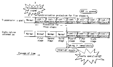
The protecting operation in a conventional system
will be explained by reference to FIG. 1. When a
failure, such as the cutoff of the signal, occurs at
time X, a signa::L with a specific bit pattern (assumed
to be fixed pattern (A)) is transmitted as an alarm
from a unit on t=he upstream side. The signal uses
alternating data, such as 010101 w , and, in many
cases, has no frame structure. Although a node which
have received this signal m.igh.t lose track of the end
position of the transmission signal frame because the
signal does not have a frame structure, the node
attempts to holc;l on until the protecting period of five
stages of frames has elapsed. 'Then, when the alarm
still lasts after the frame protecting period has
elapsed, the node senses Out cf Frame, or the collapse
of the frame synchronizatiOTl.
On the other hand, for example, the protecting
period for three stages of frames is set in the state
notice information received at the node. That is,
after the signa:L has been d_Lsconnected, the state
notice information during the normal operation is held
for up to three frames. When a change in the state
notice information is sensed a:Eter the three frames
have passed, an interrupt signal for taking in the
state notice information is generated, and the
contents of the register which holds the state notice
information are t=aken in immediately. Then, according
CA 02378413 2002-03-22
- 3 -
to the taken-in contents, an autonomous control
operation is started at the node.
After the signal has been disconnected, the bit
pattern of the state notice information is replaced
with the bit pattern of the alarm. Thus, as shown in
FIG. 1, the bit string of fixed pattern (A) has been
written in the state notice in:Eormation at the time
when the interrupt occurred. More precisely, the
bit string obtained by descrambling the bit string
010101 w of fixed pattern (A) has been written in
the state notice information.
In a conventional system, when an interrupt has
occurred, the state notice information is taken in
immediately. As a result, the bit string based on the
alarm might be mistaken for the normal state notice
information, which might therefore permit an erroneous
control operation to be performed.
As described above, in the conventional digital
signal transmis:>ion system, when a node has sensed
a change point ::gin the state notice information
protected for an n number o:E stages, this state notice
information is taken in immediately and control
according to the contents of the information is
started. When rn-stage protection is applied to the
transmission signal and the function of notifying
a downstream-side unit of the presence or absence of
a failure on the upstream s:ide by replacing the bit
CA 02378413 2002-03-22
pattern of the i~ransmission signal is provided, the
replaced bit pai~tern is taken in as state notice
information, if the expression n c m holds. That is,
there is a possibility that the process based on the
erroneously recognized state notice information will
be carried out and therefore the node will operate
erroneously.
BRIEF SUMMARY OF THE INVENTION
The object of the present invention is to provide
a node unit and a state notice information acquiring
method which el_Lminate i:he possibility of faulty
operation attributable to the erroneous recognition of
state notice information.
According to the present invention, there is
provided a node unit provided .in a digital signal
transmission system which includes a plurality of node
units for transmitting a digital transmission signal
in frame form, each frame o.f the digital transmission
signal including at least a fr<~me header indicating
the end of the signal frame, and the plurality of node
units exchanging state notice .information about
autonomous oper<~ti.on with one another, the node unit
comprising: stare notice information protecting means
for taking in the state notice information when the
state notice information co:inc.ides with predetermined n
(n is a natural number) stages of frames consecutively;
frame synchronization protecting means for protecting
CA 02378413 2002-03-22
- 5 -
the frame synchronization of the digital transmission
signal until errors are sensed consecutively over
predetermined m (m is a natural number) stages of
frames in the frame header; and information taking-in
means for, if the expression m ? n holds when the
frame synchroni:~atiorl protecting means has sensed
errors consecutively over m stages of frames in the
frame header, regarding the state notice information
included in a kwth stage (where m < k ~ 2n) frame as
valid information using the frame including the frame
header where an error first occurred as a reference and
taking in the valid information.
Errors in the frame header include not only bit
errors but also a state where the signal disappears as
a result of the disconnection of the signal cable or
the like. In short, errors mean a state where the bit
string of the previously defined frame header has been
lost.
More generally, a node unit related to the present
invention comprises information taking-in means for, if
the expression m > 2n holds when the frame synchroniza-
tion protecting means has sensed errors consecutively
over m stages of frames in the frame header, regarding
the state notice' information included in a k-th stage
(provided that k meets the expression m < k
(Int(m/n) + 1) X n, where I:nt(m/n) is an integer
obtained by disc::arding decimals of m/n) frame as valid
CA 02378413 2002-03-22
- 6 -
information using the frame including the frame header
where an error first occurred as a reference and taking
in the valid information.
5pecifical_Ly, the :information taking-in means
defers the process of taking in the state notice
information until the k-th stage frame is reached and
regards the state notice information as valid unless
the frame synchs°onization protecting means does not
sense Out of Frame in the range from the n-th stage
frame to the k-t~h stage frame.
Providing such means causes the contents of the
state notice information to be taken in after two
frames have passed since a change in the protected
state notice information was sensed, in a system with,
for example, m =-- 5 and n = 3. In the state notice
information at that time, not the bit string based on
fixed pattern (A) but a fixed signal with another bit
pattern (assumed to be fixed pattern (B)) has been
written. In th:Ls case, fixed pattern (A) is valid as
state notice information, whereas fixed pattern (B) is
invalid as state notice information.
Consequently, the process based on fixed pattern
(A) is prevented from being carried out in the node.
Specifically, it. is possible to prevent the node from
recognizing the bit string with fixed pattern (A)
based on an alarm as normal state notice information.
This eliminates the possibi:Lit.y of erroneous operation.
CA 02378413 2002-03-22
Furthermore, according to this invention, whether
the contents of the protected state notice information
are valid or not is determined according to the
presence or absence of the occurrence of OOF without
the possibility of mistakes. As a result, a faulty
operation in, for example, the protection switching
function can be prevented.
Additional objer_ts and advantages of the invention
will be set forth in the description which follows, and
in part will be obvious from the description, or may be
learned by practice of the _invention. The objects and
advantages of tine invention may be realized and
obtained by means of the instrumentalities and
combinations particularly pointed out hereinafter.
BRIEF DESCRIPTION OF THE SEVERAL VIEWS OF THE DRAWING
The accompanying drawings, which are incorporated
in and constitute a part of the specification,
illustrate embodiments of the invention, and together
with the general description given above and the
detailed description of the embodiments given below,
serve to explain the principles of the invention.
FIG. l is a time chart to help explain failure in
a conventional ordinary digital signal transmission
system;
FIG. 2 is a time chart to help explain the
operation principle related to the present invention;
FIG. 3 is <~ time chart to help explain a more
CA 02378413 2002-03-22
generalized operation principle;
FIG. 4 is a time chart to help explain the
operation princ_Lple related to the present invention;
FIG. 5 is a system diagram showing the
configuration of a digital signal transmission system
according to an embodiment of the present invention;
FIG. 6 is <~ diagram to help explain the
configuration of line cable 2;
FIG. '7 is <~ block diagram schematically showing
the configuration of the transmission unit 4 shown in
FIG. 5;
FIG. 8 is a block diagram showing the
configuration of node 3 shown in FIG. 5;
FIG. 9 is a block diagram showing the
configuration of the protection line terminal section
10 shown in FIG. 8;
FIG. 10 is a block diagram showing the
configuration of the signal processing module 17 and
subcontroller 18 of FIG. 9 in a first embodiment of
the present invention;
FIG. 11 is a time chart to help explain the
operation in the configuration of FIG. 10;
FIG. 12 is a block diagram of the signal
processing modu_Le 17 of FIG. 9 in a second embodiment
of the present :~.nvention;
FIG. 13 is a time chart to help explain the
operation in the= configuration shown in FIG. 12;
CA 02378413 2002-03-22
_ g _
FIG. 14 is a block diagram showing the
configuration of the signal processing module 17 of
FIG. 9 in a third embodiment a.f the present invention;
FIG. 15 is a time chart to help explain the
operation in the c:onfigurat.ion shown in FIG. 14;
FIG. 16 is a block diagram showing the
configuration of the signal processing module 17 of
FIG. 9 in a fourth embodiment of the present invention;
FIG. 17 is a time chart to help explain the
operation in the' configuration shown in FIG. 16; and
FIG. 18 is a block diagram showing the
configuration of the signal processing module 17 of
FIG. 9 in a fifth embodiment o:E the present invention.
DETAILED DESCRIPTION OF THE INVENTION
Hereinafter, referring to the accompanying
drawings, embod_Lments of the present invention will
be explained. Cn the embodiments, information about
an autonomous protection switching function is taken as
an example of si~ate notice information. The autonomous
protection switching function :is a function that :most
of the trunk systems have.
In a trunk system, a unit with a relay function
and others (hereinafter, referred to as a transmission
unit) may be caused to intervene between a line cable
for transmitting a transmission signal and a node.
The transmission unit has the :function of, when
a failure has occurred on the upstream side, notifying
CA 02378413 2002-03-22
- 10 -
the downstream side of the occurrence of the failure.
When sensing the occurrence of- the failure, the
transmission unit replaces the bit pattern of the
transmission signal with fixed pattern (A), thereby
notifying a node or the like on the downstream side of
the occurrence oi: the failure. Fixed pattern (A) is
characterized by having no frame structure.
If fixed pattern (A) has a meaning as state notice
information, the node interprets the meaning given in
pattern (A) and starts switching control according to
the contents. This might cause faulty operation, such
as abnormal determination or misconnection.
<Explanation of Operation Principle>
The above problem is solved on the basis of
the operation principle explained below. In the
explanation, it is assumed tha:~ the number n of
protecting stages for state notice information is n = 3
and the number rn of synchroniz<~tion protecting stages
for transmissior~i signal frames is m = 5.
The operation principle of the present invention
will be explained by reference to FIG. 2. In FIG. 2,
the letter S corresponds to the frame period of the
transmission signal and the letter T corresponds to the
frame synchronization protecting period from time X
when Out of Frame takes place :in the transmission
signal.
In FIG. 2, the letter t corresponds to a sixth
CA 02378413 2002-03-22
- 1.1
stage frame using as a reference the frame including
the frame headex° in which an error first occurred.
That is, the letter t corresponds to k when m < k
2n. The node in the embodiment takes in the contents
of the state notice information in the period t.
Furthermore, when Out of_ Frame has been sensed, an
invalid fixed pattern (B) is inserted as state notice
information. In FIG. 2, fixed pattern (B) is inserted
in the sixth stage frame and later. By doing this, the
node is prevented from operating erroneously.
A more generalized operation principle will be
explained by reference to FIG. 3. In FIG. 3, a case
with m = 7 and n = 3 is assumed. When the received
state notice inj'ormation coincides over three stages of
frames, it is loaded into a state notice information
register 25 (explained later_). A reception state
information buffer 30 (explained later), which is
realized by, for example, a shaft register, stores four
frames of state notice information.
In the normal state of th~~ system, the contents of
the state notice information are recognized on the
basis of the information stored in the state notice
information buffer 30. According to the contents, the
necessary process is executed. On the other hand, when
Out of Frame (00F) is sensed, the received state notice
information and all the contents of the state notice
information register 25 and state notice information
CA 02378413 2002-03-22
- 1.2 -
buffer 30 are considered to be state notice information
at that time and an invalid fixed pattern (B) is
inserted. Taking in the fixed pattern (B) enables
faulty operation to be prevented.
The embodiment discloses a node unit which
realizes most of_ the process based on the above
operation principle by using hardware. If the
capability of the processor is sufficient, the idea
of the present invention may he realized by software.
In this case, tlue process based on the flowchart shown
in FIG. 4 is executed by the computer.
FIG. 4 is <~ flowchart to help explain the
principle of the present invention. In FIG. 4, t:he
relationship between the setting values of m and :n is
verified in step Sl. If YES in this step, the
procedure proceeds to step S2, where k is set as shown
in the figure. In contrast, if NO in step S1, the
procedure goes t:o step S3, where k is set as shown in
the expression.
Thereafter, the procedure goes to step S4.
In step S4, if an interrupt for taking in state notice
information occurs, the procedure goes to step S5,
where the reading of state notice information about
each frame is st=arted. In step S6, it is determined
whether Out of E'rame has been sensed. If Out of Frame
has not been sensed during the time from when the
interrupt occurred until a (k - n)-th stage frame has
CA 02378413 2002-03-22
- 13 -
been read (NO in step S6), the procedure goes to step
S8, where the state notice .information during the time
from when the interrupt occurred until the (k - n)-th
state frame has been read is considered to be valid
and is processed. On the other hand, if Out of Frame
has been sensed (YES in step S6), the procedure moves
to step S7, where the state notice information during
the time from when the interrupt occurred until t:he
(k - n)-th stage frame has been read is considered to
be invalid and is discarded.
<Basic Configuration>
The basic configuration of the system shown in the
embodiment will be explained.
FIG. 5 is a system diagram showing the configura-
tion of a digital signal transmission system related to
the embodiment. The system of FIG. 5 is such that
a plurality of :>tations 1 are connected in a ring via
a line cable 2. Each station :L includes a node 3 and
transmission units 4. The node 3 is connected to the
line cable 2 via the transmission units 4. The section
sandwiched between station 1 arid station 1 is called
a segment.
As shown in FIG. 6, the line cable 2 is composed
of a service line 5 and a protection line 6. When
there is no failure in the system, that is, when the
system is in the normal state, service traffic is
transmitted via the service line 5. At this time,
CA 02378413 2002-03-22
- 1.4 -
since the protection line 6 is vacant, a low-priority
signal called part-time traffic may be allowed to flow
through the protection line 6. Each of the service
traffic and part.-time traff:i.c has the same frame
structure.
When a fai:Lure has occurred in the normal state,
the part-time traffic is pre-empted from the protection
line 6 and the service traffic is detoured to the
protection line 6. This process is realized by the
autonomous protection switching function each node 3
has, under the cooperative control of the individual
nodes 3. This ?hype of function is also called a
self-healing function.
In FIG. 6, the service line 5 is composed of a
pair of signal :Lines which transmit signals in opposite
directions and t=he protection :Line 6 is composed of
a pair of signal lines which transmit signals in
opposite directions. In the ring-like system as
shown in FIG. 5, one direction is called a clockwise
(CW) direction and the other direction is called a
counterclockwise (CCW) direction to distinguish between
them. In FIG. 6, the direction toward the right is the
CW direction and the direr_tiorx toward the left is the
CCW direction.
The concept of the upstream side and downstream
side will be explained. In FIG. 6, as for the CW line,
the transmission unit 4 is Located on the upstream
CA 02378413 2002-03-22
- 1. 5 --
side with respect to the node 3. Conversely, the node
3 is located on the downstream side with respect to
the transmission unit 4. On the other hand, as for
the CCW line, the transmission unit 4 is located on
the downstream side with respect to the node 3.
Conversely, the node 3 is located on the upstream side
with respect to the transmission unit 4.
FIG. 7 is a block diagram schematically showing
the configuration of the transmission unit 4. In
FIG. 7, the transmission unit 4 includes a signal
monitor section 7 and an alarm signal insert section 8.
The signal monit=or section '7 a.nd alarm signal insert
section 8 are provided in each of the service line 5
and the protection line 6. The signal monitor section
7 monitors the state of the traffic transmitted from
the upstream side and deterrnines whether there is
a failure or not.. When sensing the occurrence of
a failure, such as the disconnection of the cable,
the signal monitor section 7 informs the alarm signal
insert section .3 of the occurrence of the failure.
When receiving the notice of the occurrence of the
failure, the alarm signal insert section 8 inserts
an arbitrary fixed pattern in the downstream side
of the line in which the failure has been sensed.
This pattern is subjected to processes, including
scrambling. Then, the resulting pattern is transmitted
as fixed pattern (A) to the node 3.
CA 02378413 2002-03-22
- 16 -
FIG. 8 is a block diagram showing the configura-
tion of the node 3. In FIG. 8, the node 3 includes
a service line terminal section 9, a protection line
terminal section 10, a low-speed interface section 12,
a line setting section 13, a storage section 14, and
a main control section 15. The service line terminal
section 9 terminates the service line 5. The
protection line terminal section 10 terminates the
protection line 6. The low-speed interface section 12
terminates the low-speed line L1. The line setting
section 13 exch<~nges the multiplex signal introduced
into the unit via the line terminal sections 9 and 10
and low-speed lrlterface 12. The main control section
includes a C~?tJ (Central Processing Unit) (not
15 shown ) .
The service line terminal- section 9, protection
line terminal section 10, low-speed interface section
12, line setting section 13, storage section 14, and
main control section 15 are connected to one another
via an external CPU bus 16. The low-speed line 11
is connected to low-order group units, including
an exchange (noi~ shown) .
The node 3 causes the line setting section 13 to
demultiplex the time slots time-division multiplexed
with the high-order group signal transmitted via the
line cable 2 and sends the resulting signals via the
low-speed line :L1 to a low-order group unit (not
CA 02378413 2002-03-22
- 17 -
shown). The low-order group signal that has arrived
through the low--speed line 11 from a low-order unit
(not shown) is multiplexed with an arbitrary slot in
the high-order signal at the line setting circuit 13.
The resulting signal is transmitted via the line cable
2 to an adj acenl:~ node .
The main control section :15 includes switching
function control section 15a. The switching function
control section 1.5a executes the process of realizing
the autonomous protection switching function according
to a known procedure written in, for example, ITU-T
recommendation C~. 841. The function of the switching
function contro7_ section 15a is realized by software
control based on the control program stored in, for
example, the storage section 14.
FIG. 9 is a block diagram schematically showing
the configuration of the protection line terminal
section 10. The protection line terminal section
10 includes a signal processing module 17 and a
subcontroller 18. The signal processing module 17,
which terminate:> the multiplex signal introduced into
the present node via the protection line 6, carries
out various signal processes. The subcontroller 18
performs supervisory control in the protection line
terminal section 10 on the basis of the various
signals supplied from the signal processing module 17.
The signal procE~ssing module 1'7 and the subcontroller
CA 02378413 2002-03-22
- 18 -
18 are connected via an external CPU bus 16.
(First Embodiment)
Hereinafter, a first embodiment of the present
invention will be explained. Tn the first embodiment,
it is assumed that the number n of protecting stages
for state notice information is n = 3 and the number m
of synchronization protecting stages for transmission
signal frames is m = 5. Under this assumption, the
following expre:~sion holds: n ~ m < n X 2.
FIG. 10 is a block diagram showing the
configuration of the signal processing module 17 and
subcontroller 18 of FIG. 9 .in 1=he first embodiment.
In FIG. 10, the signal processing module 17 includes a
frame synchronizing pattern sensing circuit 19, a frame
synchronization protecting circuit 20, a frame counter
21, a state notice information separating circuit 22,
a state notice information protecting circuit 23,
a fixed signal insert circuit '<?4, a state notice
information regi~>ter 25, and a comparing circuit 26.
The subcontroller 18 includes a timer 27.
The frame synchronizing pattern sensing circuit 19
senses the frame synchronizing pattern of the multiplex
signal. That is, the frame synchronizing pattern
sensing circuit 19 senses a specific bit pattern
defined in the overhead of the multiplex signal.
The frame synchronization protecting circuit 20
monitors the end position of the bit pattern and
CA 02378413 2002-03-22
- i9
protects the frame synchronization of the multiplex
signal over m st=ages (m is a natural number). When the
Out of Frame has been sensed, an OOF sense signal is
output. The frame counter '~1 counts the frames of the
multiplex signa_~..
The state notice information separating circuit 22
separates and extracts state notice information about
the autonomous protection switching function from the
multiplex signal. State notice information is one
piece of the control information defined in the
overhead of the multiplex s::Lgnal. The state notice
information is i.z:>ed for enabling the control
information to be exchanged between the transmission
terminal units, including node units, to effect
protection switching. In addition, the state notice
information is also used for informing another node
unit of the alarm state.
The state notice information protecting circuit
23 protects n stages (n = 3) ef the state notice
information extracted ate the s ate notice information
separating circuit 22. When a.n OOF sense signal has
been produced, the state notice information protecting
circuit 23 resets the protection of the state notice
information.
The state notice information register 25 holds the
protective output of the state notice information from
the state notice information protecting circuit 23.
CA 02378413 2002-03-22
- GO -
When receiving the OOF signal :From the frame synchro-
nization protecting circuit 20, the fixed signal insert
circuit 24 causes the state notice information register
25 to hold a fixed signal with a specific bit string
(assumed to be ~:~ fixed pattern. (B) ) .
The compar:Lng circuit 26 senses a change point in
the protective output of_ the state notice information
from the state notice information protecting circuit
23. That is, the comparing circuit 26 compares the
protective outpl.zt of the state notice information from
the state notice information protecting circuit 23 with
the contents held in the state notice information
register 25. If they differ from each other, the
comparing circuit 26 determines that the state notice
information has r_hanged and generates an interrupt
signal. It supplies the interrupt signal to the
subcontroller 1t3.
When receiving the interrupt signal, the
subcontroller 18 supplies a taking-in signal to the
state notice information register 25 and takes in the
contents held in the state notice information register
25. Then, the subcontroller 18 supplies the contents
to the switching function control section 15a.
In the fir;~t embodiment, the subcontroller 18
includes the timer' 2~1. When receiving the interrupt
signal from the comparing circuit 26, the timer 27
starts. After counting the time equivalent to (m - n)
CA 02378413 2002-03-22
- 21 -
frames, the timer 27 generates a taking-in signal.
The operat_Lon of the above configuration will be
explained by reference to F:IG. 11. In FIG. 11, when
a signal disconnection failure has occurred at time X,
the possibility of Out of Frame arises from this time
on. Then, after five stages of protection, Out of
Frame is sensed. Moreover, after three stages of
protection from time X, the st<~te notice information
held in the stage notice information register 25
changes, with the result that an interrupt signal is
generated.
Then, this interrupt sigraal is delayed for two
frames by the fl.rnction of the timer 27. Therefore, in
the sixth stage frame, the r_ontents of the state notice
information register 25 are taken in. The taken-in
information is >upplied to the switching function
control section 15a via the external CPU bus 16.
At this tune, if contents having no meaning
as state notice information (for example, FF in
hexadecimal form) have been written in fixed pattern
(B), the switching function control section 15a regards
the contents as invalid. That is, the switching
function control section 15a considers the read
register value too be invalid state notice information
and discards it. Then, it dose not carry out the
process according to the contents of fixed pattern (B).
As a result, a i=aulty oper_aticn in, for example, the
CA 02378413 2002-03-22
- 22 -
protection switching function can be prevented.
Furthermore, in the node :3 in the first
embodiment, whet:.her the contents of the protected state
notice information are valid or not is determined
according to the presence or absence of the occurrence
of OOF without t:he possibility of a mistake. Thus, the
protection switching function can be prevented from
operating erroneously.
As described above, in the node 3 of the first
embodiment, the signal processing module 17 includes
the state notice information protecting circuit 23
which protects n (n = 3) frames of the state notice
information separated and extracted from the input
multiplex signal.., the state noi=ice information register
25 which holds t:he protected state notice information,
the comparing circuit 26 which outputs an interrupt
signal when the protected output from the state notice
information protecting circuit 23 differs from the
contents held in the state notice information register
25, the frame synchranization protecting circuit 20
which protects m (m ---- 5) frames of the multiplex
signal, the fixed signal insert circuit 24 which causes
the state notice information register 25 to hold an
invalid fixed signal as state notice information when
the frame synchronization protecting circuit 20 has
sensed OOF. The subcont:roll.er 18, which takes in the
contents held iri the state notice information register
CA 02378413 2002-03-22
- 23 -
25 in the presence of the interrupt signal output from
the comparing circuit 26, includes the timer 27 which
delays the interrupt signal. Then, after a delay time
equivalent to two frame or more and three frame or less
since the occurrence of the ini=errupt signal, the
subcontroller 18 takes in the state notice information
held in the state notice information register 25.
Since the delay time in the timer 27 is set to two
frames or more and three frames or less, when Out of
Frame takes place, the bit string of fixed patter:r~ (A)
is not taken in and fixed pattern (B) due to OOF is
taken in. Thus, the subcontroller 18 can carry out
the process according to OOF. In the normal state,
the value of the state notice information register is
protected over three frames, so that the proper value
of the state notice information can be taken in without
any omission. I~s a result, it is possible to eliminate
the possibility of a faulty operation attributable
to the erroneou.:> recognition of the state notice
information.
For examplE=, when the delay time in the timer 27
is set longer than three frame,, the value of a seventh
stage of the register. in FIc;. :L1 is taken in. In this
case, when no OOF has taken place, there is a
possibility than the state notice information present
in the range frc:~m a fourth stage to a sixth stage will
be omitted. In the first embodiment, such trouble can
CA 02378413 2002-03-22
- 24 -
be prevented.
Furthermore, in the above configuration, the state
notice information register 25 has only to buffer just
three frames. ':Chat is, the buffering of five frames
for protection is not needed, which leads to a decrease
in the hardware size.
In addition, the subcontroller 18 and main control
section 15 need not perform the following control:
determining whether the state notice information after
the buffering o:r five frames is the fixed value of OOF,
determining whether the state notice information is the
normal value or the bit string of fixed pattern (B) due
to OOF, and according to the result, switching between
the subsequent processes. As a result, the software
response process c:an be made faster.
Moreover, in the first embodiment., within one
frame from the time when Out of Frame is sensed, the
contents held in the state not..ice information register
are taken in. >etting this timing enables all the
state notice information to be sensed without any
omission, even when the state notice information
changes continu<~lly every three frames. As a result,
when the system is not in the Out-of-Frame state and
therefore is in the normal atate, control can be
performed withoi.it any troub:Le .
That is, when Out of Frame has taken place, the
bit string of fixed pattern (B) is read instead of the
CA 02378413 2002-03-22
- 25 -
bit string of fixed pattern (A). This enables control
to be performed on the basi;~ o:f OOF. Since the
contents held irn the state notice information register
are protected over three frames in the normal state,
the normal value of the state notice information can be
read at all times.
In the first embodiment, the timer 27 may be
realized in hardware by using a timer circuit with
an oscillation element. Alterwatively, it may be
a software timer. Use of a hardware timer enables the
burden of software processing on the subcontroller 18
to be reduced. C)f course, when the processor has
sufficient capability, there is no problem in using
a software timer.
(Second Embodiment)
Next, a second embodiment: of the present invention
will be explained. FIG. 12 is a block diagram of the
signal processing module 17 of FIG. 9 in the second
embodiment. In FIG. 12, the parts common to those in
FIG. 10 are indicated by the same reference numerals
and only the different parts will be explained. In the
second embodiment, the subcontroller 18 need not
include the timer 27.
In FIG. 12, the signal processing module 17
includes a (m - n) delay circuit 28 which delays the
interrupt signal generated at the comparing circuit 26
for (m - n) frames and suppliers the delayed signal to
CA 02378413 2002-03-22
_ ~y _
the subcontroller 18. Since m = 5 and n = 3 here, the
(m - n) delay circuit 28 delays the signal for two
frames.
The operation in the above configuration will be
explained by reference to FIG. 13. In FIG. 13, after
three stages of protection from time X, the state
notice information changes. Normally, an interrupt
signal would be generated at this time. In the second
embodiment, however, the (m - n) delay circuit 28
delays the interrupt signal for two frames and supplies
the delayed signal to the subc.ontroller 18.
As a result, the value in the sixth stage of the
register is read. With this reading, the timing of
taking in the contents (register value) held in the
state notice information register 25 can be made
similar to that in the first embodiment. Consequently,
the second embodiment also produces the same effect as
that of the first embodiment.
(Third Embodiment)
Next, a third embodiment of the present invention
will be explained. FIG. 14 is a block diagram of the
signal processing module 17 of FIG. 9 in the third
embodiment. In FIG. 14, the parts common to those in
FIG. 10 are indicated by the same reference numerals
and only the different parts will be explained.
In FIG. 14, the signal processing module 17
includes an n delay circuit 29 which delays the
CA 02378413 2002-03-22
G
interrupt signa_1 generated at the comparing circuit 26
for three frame:a and a state notice information buffer
30 which delays the held contents output from the state
notice informat:~on register 25 for one frame.
The operation in the above configuration will be
explained by reference to FIG. 15. In FIG. 15, after
three stages of protection from time X, the register
value of the state notice information register 25
changes. Norma).7_y, an interrupt signal would be
generated at this time. In the third embodiment,
however, the n delay circuii~ 2'~ delays the interrupt
signal for threE:~ frames. Thus, the register value of
the state notice information register 25 in the seventh
stage from time X is read.
As it stands now, however, there is a possibility
that the register value in the sixth stage of the state
notice information register 25 will be omitted. In the
third embodiment, to overcome this problem, a state
notice informat~.on buffer 3t) is provided. The state
notice information buffer 30 delays the held output
from the state notice information register 25 for one
frame, thereby Eliminating the omission of data.
The above configuration also enables the protected
state notice information within one frame from the
occurrence of OC)F to be read. Consequently, the third
embodiment also produces the same effect as those of
the first and second embodiments.
CA 02378413 2002-03-22
- 28 -
(Fourth Embodiment)
Next, a fourth embodiment: of the present invention
will be explained. FIG. 16 is a block diagram of the
signal processing module i7 of FIG. 9 in the fourth
embodiment. In FIG. 16, the parts common to those in
FIG. 14 are indicated by the same reference numerals
and only the different parts will be explained.
In FIG. 16, the signal processing module 17
includes masking section 31. The masking section 31,
which is realized in the form of, for example, a
software control function, masks the interrupt signal
about to be sent to the subcontroller 18, when an OOF
sense alarm has been given. In other words, the
masking section 31 supplies th.e interrupt signal to the
subcontroller 1f3 only when Out of Frame has not been
sensed.
The masking section 31 may be provided in the
form of a proce:>sing function :in the signal processing
module 17. Alternatively, it may be provided in the
farm of a processing function :in the subcontroller 18.
The operation in the above configuration will be
explained by reference to FIG. 17. In FIG. 17, the
interrupt signal delayed for three stages is masked at
the masking section 31. This prevents the state notice
information from being taken in. As a result, the
switching function control section 15a does not carry
out the process after the signal has been disconnected
CA 02378413 2002-03-22
_ >
~.9 -
and continues the process according to the state notice
information before the occurrence of the failure.
That is, in the fourth embodiment, the interrupt
signal after the occurrence of 00F is ignored and the
state notice information is prevented from being taken
in. This prevents the switching function control means
from carrying out the process, thereby preventing
an erroneous operation from being carried out.
In the first to third embodiments, meaningless
10 contents are written in the taken-in state notice
information, thereby indirectly preventing the
autonomous protection switching function from operating
erroneously. IT1 the fourth embodiment, however, the
state notice inaormation is prevented from being taken
15 in, thereby more directly preventing the autonomous
protection switching function from operating
erroneously. Consequently, the fourth embodiment
also makes it possible to eliminate the possibility
of a faulty operation attributable to the erroneous
recognition of i:.he state notice information.
Furthermore, in the fourth embodiment, since invalid
state notice information is not supplied to the
switching funct_Lon control section 15a, the burden of
the software processing can be reduced.
As described above, the f-first to fourth
embodiments mainly produce the following effects in
item (1) and item (2)
CA 02378413 2002-03-22
- i0 -
(1) The st<~te notice info=rmation changing
continually every three bytes cyan be sensed without any
omission.
(2) Fixed pattern (A) inserted at the time of
the disconnectic:>n of a multiplex signal with five bytes
of protection stages can be prevented from being
recognized erroneously as being effective as state
notice information.
From the items mentioned above, it is possible to
provide a node unit and a state notice information
acquiring method which eliminate the possibility of
a faulty operation attributable to the erroneous
recognition of :>tate notice information.
Whether a node unit relat=ed to the present
invention fulfi7..ls item (1) can be verified by
inputting the state notice information changing every
three bytes by an analyzer or the like and determining
whether the prot=ection switching function changes the
switching state properly.
Whether a node unit relat=ed to the present
invention fulfii7_s item (2) can be verified by
inputting 5-byte fixed pattern (B) and checking the
switching state of the protect=ion switching function.
The preseni~ invention is not limited to the above
embodiments.
For instance, in each of the above embodiments,
whether the state notice W formation after the
CA 02378413 2002-03-22
- 31 -
buffering of five frames is the fixed value of OOF, or
whether the state notice information is the normal
value or the bit: string of fixed pattern (B) due to
OOF, is determined in hardware. When the capability of
the processor is sufficient, these processes may be
executed in software.
That is, the control program following the
flowchart of FI<~. 4 is stored in, for example, the
storage section 14. On the basis of the program, the
control section 1.5 is caused to operate, which produces
a similar effecl:~ to that described above.
Although in t:he above embodiments, it has been
assumed that m =- 5 and n = 3, the values of m and n are
not restricted t:o these. For. instance, when n = 3, m
may be m = 4 or m = 3 instead of m = 5. This invention
may be applied too such a system.
Furthermore, in the embodiments, the explanation
has been given by reference to a ring network.
The idea of the present invention, however, may be
applied not only to a ring network but also to various
networks differing in topology, such as a linear
network or a me;:~h network.
Moreover, in this invention, if the frame period
of the transmitt:ed multiplex signal is S and the frame
protection period is T, when there arises a possibility
that Out of Frame of the transmission signal will occur
at time X, whether the state notice information is
CA 02378413 2002-03-22
- 32 -
valid or invalid during period. t, where X + T < t < X +
n X S X 2, may be determined on the basis of whether
Out of Frame ha~> actually occurred.
In addition, the embodiments may be applied to
a system which sends the state notice information over
a dedicated line without mu:Ltiplexing the state notice
information with a transmission signal in an embedding
manner. In this case, the transmission signal
transmitted via a line cable has only to synchronize
frame by frame with the state notice information
transmitted via the dedicated line.
In this type of system, even if the protection
switching function operates as a result of the
disconnection of the line cable, when the dedicated
line has not been disconnected, it is naturally
impossible to recognize the change point in the state
notice information as the disconnection of the cable.
In such a case, the idea of the present invention
can be applied more suitably by masking the state
notice information by a software or hardware approach
on the basis of the disconnected state of the line
cable and dedicated line. Hereinafter, an embodiment
where this invent:ion is applied to a system which sends
state notice information over a dedicated line will be
explained.
(Fifth Embodiment)
Next, a fifth embodiment of the present invention
CA 02378413 2002-03-22
- 33 -
will be explained. FIG. 18 is a block diagram of the
signal processing module 17 of FIG. 9 in the fifth
embodiment. In FIG. 18, the parts common to those in
FIG. 16 are indicated by the same reference numerals
and only the different parts wall be explained.
In FIG. 18, the input signal is a transmission
signal on a main signal line. A dedicated line carries
a state notice information signal. These signals
are designed to be transmitted over separate lines.
A frame synchronizing pattern sensing circuit 19,
a frame synchronization protecting circuit 20, and
a frame counter 21 are provided for each of the input
signal and the dedicated line. They sense the end of
each frame and apply m-stage protection. Each of the
input signal OOF sense signal and dedicated line OOF
sense signal sensed here is notified to the
subcontroller 1E3.
By carrying out a mask process using the input
signal OOF sense signal and dedicated line OOF sense
signal, the fifth embodiment. produces a similar effect
to that of the j_'ourth embodiment.
This inveni~ion may be practiced or embodied in
still other ways without departing from the spirit or
essential character thereof,
Additional advantages and modifications will
readily occur tc:> those skilled in the art. Therefore,
the invention in its broader aspects is not limited to
CA 02378413 2002-03-22
- 34 -
the specific details and representative embodiments
shown and descr_Lbed herein. Accordingly, various
modifications may be made witr~out departing from the
spirit or scope of the general inventive concept as
defined by the appended claims and their equivalents.