Note: Descriptions are shown in the official language in which they were submitted.
CA 02378551 2004-03-05
COMBINED SERIAL AND INFRARED PORT FOR CONSLIMER
ELECTRONIC DEVICES
FIELD OF THE INVENTION
The present invention relates generally to a link for interfacing host devices
with slave devices, and more particularly to a link for interfacing host
devices that
store electronic program guides (EPGs) with slave devices that enhance EPG
capabilities.
BACKGROUND OF THE INVENTION
Various means for transferring information between first and second
electronic device are known in the art, such as serial ports and infrared data
ports.
Typically, past devices have employed either a serial port, an infrared data
port, or
both ports as separate components located at separate and distinct locations.
For
example, Liukkonen et al. European Patent Application No. 898,388 describes an
apparatus for facilitating infrared data transmission between portable
electronic
devices, whereby an interconnecting cable may be employed to facilitate
communications when the infrared link does not function satisfactorily. As
another
example, Klosterman et al. PCT application WO 96!41472 teaches a television
system
having downloadable features that may be used to update out-dated software,
add new
software, and so forth.
SUMMARY OF THE INVENTION
In accordance with one aspect of the invention, there is provided a consumer
electronic device interface for use with a consumer electronic device. 'the
interface
comprises a first combined serial and infrared port included with the consumer
electronic device configured as a master, wherein a first serial signal and a
first
infrared signal share a first signal wire at the first port. The interface
further includes a
slave peripheral device comprising a second combined serial and infrared port
and an
infrared transmitter port configured as a slave and is capable of
commutucating with
the first combined serial and infrared port. A second serial signal and a
second
infrared signal share a second signal wire at the second port. The slave
peripheral
device further includes an infrared transmitter port capable of sending a
signal to an
infrared transmitter.
-1-
CA 02378551 2004-03-05
The slave peripheral device may comprise a serial debugger and/or a
demonstration ROM device and/or a database expansion device and/or a modem.
The software patches may be downloaded into the consumer elE;ctronic device
from the slave peripheral device.
The consumer electronic device may includes a televr.sion and/or a
video recorder and/or a television set top box andlor a satellite receiver
and/or a cable
box.
A demonstration interactive electronic program guide may bc~ downloaded
from the slave peripheral device to the consumer electronic device.
In one embodiment, a consumer electronic device, such as a television, cable
box, or VCR uses a combined serial and infrared output port. The combined port
is
connected to a slave peripheral device that includes a serial port and an
infrared
output port. The serial port of the slave peripheral device is comiected to
the
combined serial and infrared port and the infrared output port is cormected to
an
infrared remote control transmitter via an infrared driver signal passthrough
circuit.
BRIEF DESCRIPTION OF THE DRAWINGS
FIG. 1 is a block diagram showing a G-Link system configuration according
to one embodiment of the invention.
FIG. 2 is a lateral view of the G-Link connector according to an embodiment
of the invention.
FIG. 3 is a schematic of the G-Link/IR Out circuit located in a TV/STB
according to an embodiment of the invention.
FIG. 4 is a schematic of the interface circuit of a G-link ~~lave device
according to an embodiment of the invention.
FIG. 5 is a flow diagram of the probe request/response process according to an
embodiment of the invention.
FIG. 6 is a diagram showing different packet types of packets transmitted
between a slave and a master according to an embodiment of the invention.
FIG. 7 is a flow diagram of showing the interaction of Init, Comm and Driver
states according to an embodiment of the invention.
FIG. 8 is a flow diagram of a initial bootstrap stage according to an
embodiment of the invention.
FIG. 9 is a flow diagram of a final bootstrap process according to an
embodiment of the invention.
-la-
CA 02378551 2002-O1-04
WO 01/02942 PCT/US00/18594
FIG. 10 is a flow diagram of a bootstrap timer process according to an
embodiment of the
invention.
FIG. 11 is a flow diagram of a patch load stage according to an embodiment of
the invention.
S DETAILED DESCRIPTION
The Guide-link (G-Link) is a link that provides a serial interface between
Host devices
such as televisions (TVs) and set-top boxes (STBs), and slave devices.
Hereinafter, TV/STB
represents either a television and/or a set-top box (e.g. VCR). The G-Link
allows the
manufacturer to expand the capabilities of an EPG system by loading data and
software from a
slave device to a TV/STB. The G-Link is a cost-effective solution, as it
shares the existing IR
Mouse that is used to control televisions, cable boxes, and VCRs and uses very
few gates in the
hardware implementation.
The G-Link supports the following slave devices: a serial debugger device, a
demonstration ROM device, a database expansion device, and a modem. These
devices are not
1 S the only devices that can be supported by the G-Link. Other devices can
also be supported by
the G-Link as long as they follow the G-Link protocol.
The Serial Debugger Interface can assist in debugging production firmware,
i.e., firmware
in a TV/STB. A demonstration ROM device can download a graphical demonstration
program
that displays the features of an EPG and/or TV/STB. The demonstration ROM
device can
include customization for a retailer selling TV/STBs. A database expansion
device expands the
database information capacity of TV/STB beyond what is available in an EPG. A
modem (or an
RS-232 interface) facilitates features such as: consumer feedback, shopping,
or a worldwide web
link.
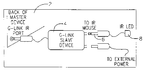
FIG. 1 shows an example of how a television, G-Link device, and IR Mouse might
be
connected. The G-Link topology is a master/slave scheme where the master
device 2 (that is, an
EPG TV/STB) interacts with one slave (that is, external) device 4. The slave
connects to the
master using the same connector 6 as an external IR Mouse. Every slave device
must have a
connector that allows an IR Mouse connection.
The G-Link slave device, when placed into an IR output mode, either passes
through the
LED drive current from the G-Link connector to the IR Mouse connector or
sources current from
its own power supply.
In the preferred embodiment of the invention, the G-Link connector 6 is a 3.5
mm (0.141
inch) mini-jack, as shown in FIG. 2 . The tip 8 of the G-Link connector is
data and the sleeve
10 of the G-link connector is ground.
FIG. 3 shows the G-Link/IR Out circuit generally located in the TV/STB.
Electrically, the
G-Link interface operates at CMOS logic levels. The output stage is an open
collector, with a
pull-up resistance of approximately SK ohms. This port is commonly shared with
the IR output
port 12 of an EPG system. The G-Link input pin of the ASIC has CMOS logic
thresholds.
-2-
CA 02378551 2002-O1-04
WO 01/02942 PCT/US00/18594
1 Tables 1 through 3 show the DC characteristics for G-Link in the preferred
embodiment
of the invention. Table 1 shows the absolute maximum input voltage at the
connector. Tables
2 and 3 assume Vdd = S.OOV. Table 2 shows the valid logic input levels. Table
3 shows the
output voltage at the connector.
Logical'Value Condition Min (V) Max (V)
Any CMOS Vss-0.3 Vdd+0.3
Table 1
Logieal ConditionMin Max
Value (V) (V)
Zero CMOS 1.5
One CMOS ~
3.5
Table 2
I Logical ConditionMin (V) Max
Value (V)
Zero Ion _- 0.4
10
mA
One IoH = 4.0
0.1
Table 3
For electrostatic discharge (ESD) protection and noise filtering, the rise
time of the G-
Link signal should not exceed 5 ~cS. Since the total pull-up resistance is
about 5K ohms, in
some configurations this allows for 220pF of filter capacitance 14 to ground
at each end of
the G-Link wire. The series resistance of the G-Link cable connection should
remain below
50 ohms.
The 270ohm resistor 20, shown in FIG. 3, protects the ASIC from Electrostatic
dischar a ESD . The 220 F ca acitor also hel s rotect the ASIC. T icall a s
ark a or
g ~ ) P p P P Yp Y~ p g P
other device is also added to satisfy manufacturer ESD standards.
In the preferred embodiment, the ASIC input pins can withstand the following
ESD
tests: 200 V from a 200pF capacitor with no series resistance; and 1.OK V from
a 100pF
capacitor with a 1.5K series resistance.
The G-Link and the IR output device share the same port. The IR output
circuit,
which typically shares the same connector with the G-Link port, consists of a
high-side driver
-3-
CA 02378551 2002-O1-04
WO 01/02942 PCT/US00/18594
1 transistor. This transistor pulls the output up to Vcc through a current
limiting resistor-the
value of which depends on the particular IR output device. The IR and G-Link
outputs can
never be asserted at the same time.
G-Link devices may take a variety of forms. A G-Link slave device can be
powered
by a separate external power source. A low-power G-Link slave device can be
without an
external power source. FIG. 4 shows the minimum required interface components
for a G-
Link device in a preferred embodiment of the invention.
In the preferred embodiment, the G-link hardware transmits asynchronously at
38400
bps using RS-232-type start and stop bits. Characters are transmitted with 8
data bits, no
parity, and I stop bit (8N1). In alternative embodiments, the G-link hardware
transmits at
higher bps rates and may encode characters in any encoding scheme known to one
with
ordinary skill in the art.
The G-link follows the International Standards Organization Open Systems
Interconnection (ISO/OSI) model for networks. The Transport layer in the Open
Systems
Interconnection (OSI) model resides between the Network and Session layers.
The Transport
layer controls the sequence of packets, regulates packet flow, and recognizes
duplicate
packets.
An error in a packet is indicated by a negative acknowledgment (NACK). If an
error
occurs in a packet (HACK), the Session layer must initiate a retransmission
request.
Table 4 and Table S defines the general formats for all Request and Response
packets
in a preferred embodiment of the invention. Table 4 defines the Request Packet
Format in a
preferred embodiment. Table 5 defines the Response Packet Format in a
preferred
embodiment. In alternative embodiments, the Start-of Packet (SOP) byte,
Request Command
byte, Data Block Length Byte, Sequence Low/Sequence High, and Data Block
within may
occur in any order, except that the Data Block Length must be before the Data
Block. EOP
is End-of Packet.
Byte Meaning
Number
0 SOP byte - 0x07
1 Re uest Command B to
-4-
CA 02378551 2002-O1-04
WO 01/02942 PCT/US00/18594
1 2 Data Block Length Byte (number of payload bytes
to follow, including EOP and
Checksum; number of data bytes may be zero)
3-4 Sequence Low/Sequence High. These bytes are included
only if DS of the Packet Type
is set. These bytes are not included in the data
block length count.
S-N Data Block (this block may contain zero bytes)
(last-1) EOP byte - OxBF
(last) Checksum (Zero indicates checksum not calculated.
A zero checksum is mapped onto
OxFF.). Checksum (calculated by adding all bytes
and checksum mod256=0) includes
all bytes above, from SOP through EOP.
Table 4
Byte Meaning,
Number
0 SOP byte - 0x07
1 Response Command Byte
2 Data Block Length Byte (number of payload bytes
to follow, including EOP and
Checksum; number of data bytes may be zero)
3-4 Sequence Low/Sequence High. These bytes are included
only if DS of the Packet Type
is set. These bytes are not included in the data
block length count.
5-N Data Block (this block may contain zero bytes)
(last-1) EOP byte - Ox8F
(last) Checksum (Zero indicates checksum not calculated.
A zero checksum is mapped onto
OxFF.). Checksum (calculated by adding all bytes
and checksum mod256=0) includes
all bytes above, from SOP through EOP.
fable 5
Every G-Link data transaction is a request/response packet sequence between
the
master and the slave. In most cases, the master initiates G-Link transactions
(that is, the EPG
device) that are acted upon by the slave (that is, the external device). A
slave device must
Process, at a minimum, eight bytes of transmit and receive buffer data. There
are three
reasons for using this transaction method: (1) eases the implementation over a
dual-simplex
data link; (2) reduces the chance of data request collisions; and (3)
eliminates potential
problems when IR and G-Link share the same port-slave transactions respond
with a
Negative Acknowledgment (NACK) bit or interfere with IR operation.
A request/response packet sequence may be either a write request (where data
is
carried in the request) or read request (where data is contained in the
corresponding response).
All valid request packets return an Acknowledge (ACK) response packet to the
-5-
CA 02378551 2002-O1-04
WO 01/02942 PCT/US00/18594
1 requester. When the transport layer of the responding device detects an
error condition (for
example, no valid SOP/EOP, invalid checksum, time-out, invalid command), a
NACK
response packet is returned to the requester.
In the event of a NACK response, the transport layer will not initiate a
retry. The
Session layer that resides on top of the transport layer is responsible for
initiating a retry
packet request. Either the master or slave can execute the packet retry.
In the preferred embodiment of the invention, a data block can be a maximum of
255
bytes. When a transaction has more data than can fit into one 255-byte data
block, that data
must be divided into a sequence of packets. Packet sequence numbers start at
zero and
monotonically increase as necessary. Data transfer must occur in order if the
data block sizes
within a packet are different sizes.
Although the transport layer controls the order of the packets, the request
and
response packets must include a Sequence Present bit and the packet sequence
numbers.
In alternative embodiments of the invention, a data block can be greater than
255
bytes. Alternative embodiments can have data blocks that have a maximum of 2"-
1 bytes,
where n>8.
Table 6 lists the standard G-Link device commands supported by all G-Link
devices.
Write RequestCommand Read RequestCommand
~
Probe 0x80 Probe 0x40
Memory 0x47 Memory 0x48
Identify 0x41 Identify 0x01
Table 6
The G-Link probe process involves G-Link master device routinely sending a
Probe
Request packet that looks for the presence of a G-Link slave device. If a
device is present,
the slave sends a Probe Response packet.
FIG. 5 shows the probe request/response process. In the preferred embodiment
of the
invention, the Master sends a probe request packet every minute 30 until a
probe response
packet is sent by the slave. If there is no slave device present, then there
will be no response
32. If a slave device is attached 34 and if it is operable, then it will send
a Probe Response
packet 38 in response to a Probe Request packet 36. The Probe Response packet
includes
-6-
CA 02378551 2002-O1-04
WO 01/02942 PCT/US00/18594
1 speed and buffer size information. After receiving the Probe Response
packet, the Master
will adjust the speed and buffer size if the slave speed and buffer size
information is different
from the speed and buffer size information that the Master has 40.
Once a Probe Request and Response packet exchange has occurred between the
master and slave, the master no longer sends a Probe Request packet-unless the
slave does
not respond to any other request-packet type, in which case the master re-
initiates the Probe
Request sequence.
In the preferred embodiment, the G-Link master supports only one slave device
connection at a time. In alternate embodiments, the G-Link master may support
more than
one slave device, wherein a priority scheme is implemented to determine which
device shall
have access to the G-Link.
Link speed and buffer size are determined through the exchange of the Probe
Request
and Probe Response packets. The G-Link master sends a Probe Request packet
with a default
speed of 38400 bps and a buffer size of 255 bytes. The slave responds with a
Probe Response
packet defining its maximum transmission speed and buffer size. Table 7 lists
the Probe
Request packet format and Table 8 lists the Probe Response packet format.
~, Byte Number: ~ .Meaning
0 0x80
Table 7
Byte NumbexMeaning
0 SOP byte - 0x07
1 0x40
2 Data Block Length Byte - 0x04
3 Baud Rate
D7-D2: Reserved
[D 1:D0]
00 4800
3 O 1 9600
S
10 19200
11 38400
-
CA 02378551 2002-O1-04
WO 01/02942 PCT/US00/18594
1 4 Maximum Receive Buffer Size - 0x8 to OxFF
EOP byte - OxBF
6 Checksum
Table 8
The Master Request Format packet 50 is a generic request packet where the
master
asks the slave "do you have anything to send?" The advantage of this packet
type is it allows
the slave to respond without waiting for the master to send a specific request
packet type (for
example, the slave would only send an Identify Response packet after it
received an Identify
Request packet). FIG. 6 shows the different types of packets a slave could
send in response
to the Master Request Format packet. A slave device will still respond to a
specific request
packet type (that is, the slave sends an Identify Response packet after the
master sends an
Identify Request packet).
The slave can respond to a Master Request Format Packet with an Identify
Response
packet 52, a memory read followed by a Request packet 54, or a Retry packet
followed by a
Request packet 56.
The Identify Request and Identify Response packets are used to identify the
slave
device type. The Identification Response packet, as shown in Table 10,
contains the
following data: a device type/subtype and a null-terminated string describing
the device. The
device type/subtype data may be used by operational firmware to discern what
slave device is
installed on G-Link. The null-terminated string may be used by Factory
Test/Diagnostics
screens. Table 9 lists the Identification Request Packet format and Table 10
lists the
Identification Response Packet format.
Byfe Number:Meaning
0 SOP byte - 0x07
1 0x41
2 Data Block Length Byte (0x02= no data block present)
3 EOP byte - OxBF
4 Checksum
Table 9
ByEe Number ~ Meaning
0 SOP bvte - 0x07
_g_
CA 02378551 2002-O1-04
S
WO 01/02942 PCT/US00/18594
1 0x01
2 Data Block Length - 0x02
3 EOP byte - OxBF
4 Checksum
Table 10
Byte NumberMeaning
0 SOP byte - 0x07
1 Packet Type/Flag Byte
D7: b' 1' - Request Packet
D6: b'0' - Read Request
D5: b' 1' - Sequence field present
D4-D0: Ob00010: Load Driver Command
2 Data Block Length Byte
3 EOP byte - Ox8F
4 Checksum
Table 11
Byte Number Meaning
p SOP byte - 0x07
1 0x48
2 Data Block Length Byte - 0x02
3-5 Source Address (Preferred: Big Endian)
6 NUMBYTESTOREAD
7 EOP byte - Ox8F
8 Checksum
Table 12
Memory Write Packet Format
The Memory Write Request packet is a request-only packet initiated by the
slave.
This packet tells the master where and how much data the slave wants to store
in the master.
The master does not send a response packet. Table 13 lists the Memory Write
Request Packet
format.
-9-
CA 02378551 2002-O1-04
WO 01/02942 PCT/US00/18594
1 Byte Number'Meaning
0 SOP byte - 0x07
1 0x47
2 Data Block Length Byte - 0x02
3-5 Source Address (Big Endian)
6 NUMBYTESTOWRITE
7-N Write Data Block
(last-1) EOP byte - OxBF
(last) Checksum
Table 13
The G-Link has state conditions for packets. Different packet types operate in
various
states. A packet type may be used in one or more of the following three
states: Initial (Init),
Communication (Comm), and Driver. In the Initial state probe packets are
passed. In the
Communication state, data, get next, and retry packets are passed. In the
Driver state, driver
packets are passed.
The type of packet sent in a state depends on which Master and Slave events
are used.
Master events are originated from the Slave. Slave events are originated from
the Master.
Master and Slave events and their corresponding designations are listed in
Table 14.
25
35
-10-
CA 02378551 2002-O1-04
WO 01/02942 PCT/US00/18594
1 Master ' Event Name Slave Event Event blame
Event Designation
Designation
A Other i Other
B Timeout Probe ii Initial Probe
C Probe Response iii Get T~Text
D Request-Read iv Timeout
E Request' Write v Factory Test
Request
F Load Driver vi Retry
G Execute vii Miss Byte
H IR Received
I Factory Test
Response
1 Miss Byte
K Reset Protocbl
L Timeout Data
Table 14
Not all master events are allowed in every state. Table 15 indicates (using a
~) which
Master events are allowed in each state.
A B C D E F G H I J K L
Init State
Comm State , , , , , , , , , ,
Driver , , , , , ,
State
Table 15
FIG. 7 shows an example of how packets and events interact in the three
states. In the
Initial state probe packets are passed. In the Communication state, data, get
next, and retry
packets are passed. In the Driver state, driver packets are passed.
In the initial state 60, the slave device ignores Master events A, and D
through L as
shown in Table 15 61. The Master does an initial probe of the slave 62. If the
slave responds
to the initial probe, then the probe packet was successful and the
Communication State is
entered 63. If the probe packet is not successful, then the Master sends a
timeout probe to the
slave and the slave has a timeout 64. Then, the Master sends a retry packet to
the slave and
the slave does a retry 65. The slave attempts to respond to the retry packet,
whereupon the
-11-
CA 02378551 2002-O1-04
WO 01/02942 PCT/US00/18594
1 initial state 60 is entered and the Master does another initial probe of the
slave 62.
In the Communication State, the slave formats the next packet to give to the
Master
66. In the Communication State, the slave ignores Master events A (Other) and
C (Probe
Response) 67.
There are four paths that the Communication State can take. In one path, the
Master
requests the next packet from the slave 68. Then, the slave does a request
read and the master
responds with the data from the specified address.
In a second path, the Master requests the next packet from the slave 70. The
slave
writes the packet 71. There is just one "next packet request" instead of both
a "next packet
request" and a "master request for a write." A checksum is checked to see if
it is valid 72. If
the checksum is not valid, then there is a retry of a packet write from the
slave to the Master
~d the slave attempts a retry 73. Another possibility is that one or more
bytes are missed by
the slave and the master times out waiting for the expected number of bytes to
be received. In
this case, the slave also times out.
When there is a retry of a packet 74, a retry packet counter is checked 75. If
the retry
Packet counter is greater than zero, then the master sends a retry packet to
the slave 76. If the
retry packet counter is not greater than zero, then the Initial state is
returned to 77. The
"Initial State" is a cold reset of the Master. At this point, the Master
assumes that the slave
has hung up in the middle of uploading a patch, and the Master attempts to
purge its memory
with this Cold Reset.
In a third path, the Master requests the next packet from the slave 78. The
Driver
State is entered 79 and Master events A, F, G, H, I, and J are ignored 80. The
Master begins
to load the driver from the slave, packet by packet. A test is conducted for
whether there are
more packets 81. Just in case the same packet is sent twice correctly by the
slave, the master
counts it as only one packet received. Packet zero provides the total size 82.
If there are more
packets to be sent, then the slave continues to send packets to the Master. If
there are no
more packets to be sent, then the slave sends an execute packet and the Master
executes the
sent packets 83 whereupon the Initial state is returned to 84.
In a fourth path, the Master requests the next packet from the slave 85. The
slave
sends an execute packet and the Master executes the packet 83 whereupon the
Initial state is
returned to 84.
-12-
CA 02378551 2002-O1-04
WO 01/02942 PCT/US00/18594
1 From either the Communication State or the Driver State, the slave can Reset
Protocol
in which case the Master resets the protocol 86 or the slave can timeout, in
which case the
Master has a Factory Test Response 87.
A patch download from a slave device to a TV/STB comprises three stages. The
three
stages in the bootstrap process are (1) Initial Bootstrap; (2) Final
Bootstrap; and (3) Patch
Load. Each stage provides items that are used in the next stage. The preceding
stage must be
successfully completed before the next one can begin.
Stage 1 is the Initial Bootstrap stage. The Initial Bootstrap stage provides
the
essential tools used in the Stage 2, Final Bootstrap stage. FIG. 8 shows the
initial bootstrap
stage. After the successful completion of the initial bootstrap stage, the
following items are
available for use in the next stage: Faster probe packets (every .5 seconds),
Watchdog timer,
1 S ~d End of stage packet handler.
At the beginning of the initial bootstrap stage, the Slave device is in its
initial state
110. The TV/STB, which is a G-link master device, routinely sends to the slave
device, a
probe request packet 111 that looks for the presence of a G-link slave device.
In a preferred
embodiment of the invention, if the TV/STB determines within 5.6 seconds 112
that the slave
device is present, then the slave device sends an identify response packet
113. The TV/STB
requests the next packet from the slave device 114. In a preferred embodiment
of the
invention, if the slave device responds within 5.6 seconds to the next packet
request 115, then
the slave device does a memory write to its memory 116. The TV/STB sends
another probe
request packet to the slave device 117. The slave device does a memory write
to the TV/STB
that causes the TV/STB to "execute" the instructions within the memory write
118. The
TV/STB executes the instructions contained within the memory write from the
slave device
119.
Stage 2 is the Final Bootstrap stage. FIG. 9 shows the Final Bootstrap
process. The
final bootstrap stage provides the patch information that is loaded in the
third stage. After the
successful completion of the Final Bootstrap stage, at least the following
items are available:
TV screen display that shows real-time download percent complete, watchdog
timer
(replaces watchdog timer from stage 1 );
Get Next packet (suppresses Probe packets from stage 1 );
End of stage packet handler (replaces End of stage packet from stage 1);
-13-
CA 02378551 2002-O1-04
WO 01/02942 PCT/US00/18594
Retry packet; and
size of a final patch.
At the beginning of the final bootstrap stage, the TV/STB sends a probe
request
packet to the slave device 120. In a preferred embodiment of the invention,
the TV/STB
determines within .5 seconds whether the slave device has responded to the
TV/STB 121. If
the slave device does respond within .5 seconds, then the slave device does a
memory write
122 until the end of the final bootstrap stage 123. At the end of the final
bootstrap stage, the
instruction within the memory-writes are executed by the TV/STB 124.
FIG. 10 shows the 20-second timer flowchart, which is applicable in a
preferred
embodiment of the invention. During the final bootstrap stage, if a 20-second
timer expires
130, then the bootstrap process returns to the initial bootstrap stage 131,
otherwise the
bootstrap process is proceeding properly 132.
Stage 3 is the Patch Load stage. FIG. 11 shows the patch load stage. The patch
load
stage arranges the information from the first two stages into usable patch
code. At the
beginning of the patch load stage, the TV/STB gets a new packet from the slave
device 140.
The slave device does a memory write from its memory to the TV/STB 141. The
TV/STB
determines whether the packet has been successfully received by the TV/STB
within a timer
period 142. In the preferred embodiment of the invention, the timer period is
three seconds.
If the timer period expires 143, then the packet was not successfully
transferred from the
slave device to the TV/STB. If the packet is determined to be successfully
received, then the
timer period is reset 144, the displayed percentage completed on the
television screen is
incremented 145, and the TV/STB gets the next packet from the slave device
140. When the
patch load end of stage is reached 146, the TV/STB goes into a patch load warm
reset state.
den the timer period expires 143, then the TV/STB determines whether a retry
counter is
greater than zero 150. The retry counter represents the number of times the
TV/STB will
retry a packet request because of the timer period expiration. If the retry
counter is greater
than zero, then the TV/STB will request another packet from the slave device
151. If the
retry counter is not greater than zero, then the retry counter has been
exhausted and the
bootstrap process returns to stage 1, the Initial Bootstrap stage 152.
-14-