Note: Descriptions are shown in the official language in which they were submitted.
CA 02378722 2002-O1-07
WO 01/05071 PCT/GB00/02632
1
SIGNALLING SYSTEM
The present invention relates to a signalling system. The
invention has particular, although not exclusive,
relevance to the provision of a duplex free space optical
communication system.
The applicant has proposed in their earlier International
Application WO 98/35328 a point to multipoint data
transmission system which uses a retro-reflector to
receive collimated laser beams from a plurality of user
terminals, to modulate the received laser beams and to
reflect them back to the respective user terminals. This
point to multipoint data transmission system employs
pixelated reflector/modulator arrays and a telecentric
optical lens system. Each pixel in the array maps to a
unique angular position in the field of view of the
telecentric optical lens system. Communications with
each of the user terminals is then achieved using the
appropriate pixel in the array which maps to the
direction in which the user terminal is located within
the field of view.
WO 98/35328 teaches the use of an array of Quantum
Confined Stark Effect (QCSE) modulators and a separate
array of photodiodes. This earlier application also
teaches that the photodiodes and the modulators may be
provided in a single array. WO 98/35328 also teaches
that a low bandwidth control channel may be established
CA 02378722 2002-O1-07
WO 01/05071 PCT/GB00/02632
2
between the rectro-reflector and the user terminals by
adding a small signal modulation to the laser beam
transmitted from the user terminals. However, this
results in asymmetric bandwidths for the uplink data and
the downlink data.
According to one aspect, the invention aims to provide an
optical free space communication system having an
increased uplink bandwidth for data transmitted from the
user terminal to the retro-reflector. According to
another aspect, the invention aims to provide an
increased bandwidth for downlink data transmitted from
the retro-reflector to the user terminal. According to
another aspect, the invention provides a full duplex free
space optical communication system having symmetrical
bandwidth available for the uplink and downlink data.
According to another aspect, the invention aims to
simplify the system described in WO 98/35328.
Exemplary embodiments of the inventions will now be
described with reference to the accompanying drawings in
which:
Figure 1 is a schematic diagram of a video broadcast
system for supplying video signals for a plurality of
television channels, to a plurality of remote users;
Figure 2 is a schematic block diagram of a local
distribution node and a user terminal which forms part of
CA 02378722 2002-O1-07
WO 01/05071 PCT/GB00/02632
3
the video broadcast system shown in Figure l;
Figure 3 is schematic diagram of a retro-reflector array
and lens system employed in the local distribution node
shown in Figure 2;
Figure 4 is a schematic diagram of a pixelated modulator
array forming part of the retro-reflector array and lens
system shown in Figure 3;
Figure 5a is a cross-sectional view of one modulator of
the pixelated modulator shown in Figure 4, in a first
operational mode when no DC bias is applied to electrodes
thereof;
Figure 5b is a cross-sectional view of the modulator
shown in Figure 5a, in a second operational mode when a
bias voltage is applied to the electrode;
Figure 6 is a signal diagram which illustrates the way in
which light incident on the modulators shown in Figure 5
is modulated in dependence upon the bias voltage applied
to the modulator electrodes;
Figure 7 is a block diagram illustrating the principal
components of the bias voltage driving circuitry and the
detection circuitry which is coupled to the electrodes of
the modulator shown in Figure 5;
CA 02378722 2002-O1-07
WO 01/05071 PCT/GB00/02632
4
Figure 8 is a schematic diagram of a local distribution
node and a user terminal which forms part of a data
distribution system similar to that shown in Figure 1;
Figure 9 is a schematic diagram of the main optical
components of the user terminal shown in Figure 8;
Figure 10 is a schematic view of the local distribution
node shown in Figure 8;
Figure 11 is a plot illustrating the way in which the
laser power is varied to achieve a small signal
modulation for uplink data transmitted from a user
terminal to a local distribution node;
Figure 12 is an eye diagram illustrating the effect of
the small signal modulation on the downlink data
transmitted from the local distribution node to the user
terminal;
Figure 13 is a schematic circuit diagram illustrating the
way in which the modulator shown in Figure 5 can be
operated to modulate a received laser beam with data and
to simultaneously detect data carried by the received
laser beam;
Figure 14 is a schematic diagram illustrating the
principal components of a user terminal which may be used
in a communications system similar to that shown in
CA 02378722 2002-O1-07
WO 01/05071 PCT/GB00/02632
Figure 1; and
Figure 15 is plot illustrating the way in which the
reflectance of a QCSE modulator varies with the
5 wavelength of the incident light.
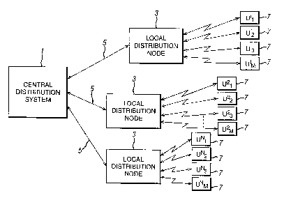
Figure 1 schematically illustrates a video broadcast
system for supplying video signals, for a plurality of
television channels, to a plurality of remote users. As
shown in Figure 1, the system comprises a central
distribution system 1 which transmits optical video
signals to a plurality of local distribution nodes 3 via
a bundle of optical fibres 5. The local distribution
nodes 3 are arranged to receive the optical video signals
transmitted from the central distribution system 1 and to
transmit relevant parts of the video signals to
respective user terminals 7 (which are spatially fixed
relative to the local distribution node 3) as optical
signals through free space, i.e. not as optical signals
along an optical fibre path.
In this embodiment, the video data for all the available
television channels is transmitted from the central
distribution system 1 to each of the local distribution
nodes 3, each user terminal 7 informs the appropriate
local distribution node 3 which channel or channels it
wishes to receive (by transmitting an appropriate
request) and, in response, the local distribution node 3
CA 02378722 2002-O1-07
WO 01/05071 PCT/GB00/02632
6
transmits the appropriate video data, to the respective
user terminals 7. Each local distribution node 3 does
not, however, broadcast the video data to the respective
user terminals 7. Instead, each local distribution node
3 is arranged (i) to receive an optical beam transmitted
from each of the user terminals 7 which are in its
locality, (ii) to modulate the received beams with the
appropriate video data for the desired channel or
channels, and (iii) to reflect the modulated beams back
to the respective user terminals 7. In addition to being
able to receive optical signals from the central
distribution system 1 and from the user terminal 7, each
of the local distribution nodes 3 can also transmit
optical data, such as status reports, back to the central
distribution system 1 via the respective optical fibre
bundle 5, so that the central distribution system 1 can
monitor the status of the distribution network.
Figure 2 schematically illustrates in more detail the
main components of one of the local distribution nodes 3
and one of the user terminals 7 of the system shown in
Figure 1. As shown in Figure 2, the local distribution
node 3 comprises a communications control unit 11 which
(i) receives the optical signals transmitted along the
optical fibre bundle 5 from the central distribution
system 1; (ii) regenerates the video data from the
received optical signals; (iii) receives messages 12
transmitted from the user terminals 7 and takes
appropriate action in response thereto; and ( iv ) converts
CA 02378722 2002-O1-07
WO 01/05071 PCT/GB00/02632
7
the appropriate video data into data 14 for modulating
the respective light beams 15 received from the user
terminals 7. In converting the video data into
modulation data 14, the communications control unit 11
will encode the video data with error correction coding
and coding to reduce the effects of inter-symbol-
interference and other kinds of well known sources of
interference such as from the sun and other light
sources.
The local distribution node 3 also comprises a retro-
reflector and modem unit 13, which is arranged to receive
the optical beams 15 from the user terminals 7 which are
within its field of view, to modulate the respective
light beams with the appropriate modulation data 14 and
to reflect the modulated beams back to the respective
user terminals 7. In the event that an optical beam 15
received from one of the user terminals 7 carries a
message 12, then the retro-reflector and modem unit 13
retrieves the message 12 and sends it to the
communications control unit 11 where it is processed and
the appropriate action is taken. In this embodiment, the
retro-reflector and modem unit 13 has a horizontal field
of view which is greater than +/- 50° and a vertical
field of view of approximately +/- 5°.
Figure 2 also shows the main components of one of the
user terminals 7. As shown, the user terminal 7
comprises a laser diode 17 for outputting a laser beam 19
CA 02378722 2002-O1-07
WO 01/05071 PCT/GB00/02632
8
of coherent light. In this embodiment, the user
terminals 7 are designed so that they can communicate
with the local distribution node 3 within a range of 150
metres with a link availability of 99.9 per cent. To
achieve this, the laser diode 17 is a 50 mW laser diode
which outputs a laser beam having a wavelength of 850 nm.
This output laser beam 19 is passed through a collimator
21 which reduces the angle of divergence of the laser
beam 19. The resulting laser beam 23 is passed through
a beam splitter 25 to an optical beam expander 27, which
increases the diameter of the laser beam for transmittal
to the retro-reflector and modem unit 13 located in the
local distribution node 3. The optical beam expander 27
is used because a large diameter laser beam has a smaller
divergence than a small diameter laser beam.
Additionally, increasing the diameter of the laser beam
also has the advantage of spreading the power of the
laser beam over a larger area. Therefore, it is possible
to use a higher powered laser diode 17 whilst still
meeting eye-safety requirements.
Using the optical beam expander 27 has the further
advantage that it provides a fairly large collecting
aperture for the reflected laser beam and it concentrates
the reflected laser beam into a smaller diameter beam.
The smaller diameter reflected beam is then split from
the path of the originally transmitted laser beam by the
beam splitter 25 and focussed onto a photo-diode 29 by a
lens 31. Since the operating wavelength of the laser
CA 02378722 2002-O1-07
WO 01/05071 PCT/GB00/02632
9
diode 17 is 850nm, a silicon avalanche photo-diode (APD)
can be used, which is generally more sensitive than other
commercially available photo detectors, because of the
low noise multiplication which can be achieved with these
devices. The electrical signals output by the photo-
diode 29, which will vary in dependence upon the
modulation data 14, are then amplified by the amplifier
33 and filtered by the filter 35. The filtered signals
are then supplied to a clock recovery and data retrieval
unit 37 which regenerates the clock and the video data
using standard data processing techniques. The retrieved
video data 38 is then passed to the user unit 39, which,
in this embodiment, comprises a television receiver in
which the video data is displayed to the user on a CRT
(not shown).
In this embodiment, the user unit 39 can receive an input
from the user, for example indicating the selection of a
desired television channel, via a remote control unit
(not shown). In response, the user unit 39 generates an
appropriate message 12 for transmittal to the local
distribution node 3. This message 12 is output to a
laser control unit 41 which controls the laser diode 17
so as to cause the laser beam 19 output from the laser
diode 17 to be modulated with the message 12. As those
skilled in art will appreciate, in order that the data
being transmitted in opposite directions do not interfere
with each other, different modulation techniques should
be employed. For example, if the amplitude of the laser
CA 02378722 2002-O1-07
WO 01/05071 PCT/GB00/02632
beam 15 is modulated by the local distribution node 3,
then the laser control unit 41 should modulate, for
example, the phase of the transmitted laser beam.
Alternatively, the laser control unit 41 could apply a
5 small signal modulation to the laser beam 19 to create a
low-bandwidth control channel between the user terminal
7 and the local distribution node 3. This is possible
provided the detector in the local distribution node 3
can detect the small variation in the amplitude of the
10 received laser beam. Furthermore, such a small signal
amplitude modulation of the laser beam would not affect
a binary "on" and "off" type modulation which could be
employed by the retro-reflector and modem unit 13.
The structure and function of the components in the user
terminal 7 are well known to those skilled in the art and
a more detailed description of them shall, therefore, be
omitted.
Figure 3 schematically illustrates the retro-reflector
and modem unit 13 which forms part of the local
distribution node 3 shown in Figure 2. As shown, in this
embodiment, the retro-reflector and modem unit 13
comprises a wide angle telecentric lens system 51 and an
array of modulators/detectors 53. The design of such a
wide angle telecentric lens using fisheye lens techniques
is well known to those skilled in the art. In this
embodiment, the telecentric lens 51 comprises lens
elements 51 and 55 and a stop member 57, having a central
CA 02378722 2002-O1-07
WO 01/05071 PCT/GB00/02632
11
aperture 59. The size of the aperture 59 is a design
choice and depends upon the particular requirements of
the installation. The structure and function of the
telecentric lens system is described in the applicants
earlier International application WO 98/35328, the
contents of which are incorporated herein by reference.
As illustrated in Figure 3 by the two sets of ray bundles
67 and 69, laser beams form different sources are
focussed onto different parts of the array of
modulators/detectors 53. Therefore, by using an array of
separate modulators/detectors 53, the laser beams 15
from all the user terminals 7 can be separately detected
and modulated by a respective modulator/detector. Figure
4 is a schematic representation of the front surface
(i.e. the surface facing the lens system 51) of the
modulator/detector array 53 which, in this embodiment,
comprises 100 columns and 10 rows of modulator/detector
cells ci~ (not all of which are shown in the Figure). In
this embodiment, the size of the cells ci~ is between 50
and 200 pm with a spacing (centre to centre) 72 between
the cells being slightly greater than the cell size 71.
The telecentric lens 51 is designed so that the spot size
of a focussed laser beam from one of the user terminals
7 corresponds with the size 71 of one of the
modulator/detector cells ci~, as illustrated by the
shaded circle 73 shown in Figure 4, which covers the
CA 02378722 2002-O1-07
WO 01/05071 PCT/GB00/02632
12
modulator/detector cell cz2. In this embodiment, Quantum
Confined Stark Effect (QCSE), sometimes also referred to
as Self Electro-optic Effect Devices or SEEDs) devices,
developed by the American Telephone and Telegraphic
Company (AT&T) , are used for the modulator/detector cells
ci~ . In particular, the QCSE devices are used to both
modulate the incident laser beam and to detect the
received laser beam. In the applicants earlier
International application WO 98/35328 QCSE devices were
used only to modulate the received light beam. Separate
photodiodes were used to detect the received laser beam.
However, this embodiment makes use of the fact that the
QCSE modulator device comprises a p-i-n diode and
therefore can also detect light incident on it. As will
be described in more detail below, in this embodiment,
half-duplex communications links between the local
distribution nodes and the user terminals are established
using the QCSE modulators.
Figure 5a schematically illustrates the cross-section of
the QCSE device 79. As shown, the QCSE device comprises
a transparent window 81 through which the laser beam 15
from the appropriate user terminal 7 can pass followed by
three layers 83-1, 83-2 and 83-3 of Gallium Arsenide
(GaAs) based material. Layer 83-1 is a p conductivity
type layer, layer 83-2 is an intrinsic layer and layer
83-3 is an n conductivity type layer. Together, the
three layers 83-1, 83-2 and 83-3 form a p-i-n diode. As
shown, the p conductivity type layer 83-1 is connected to
CA 02378722 2002-O1-07
WO 01/05071 PCT/GB00/02632
13
the electrode 89 and the n conductivity type layer 83-3
is connected to the ground terminal 91. As shown in
Figure 5a, a reflective layer 85 is provided beneath the
n type conductivity layer 83-3 and beneath this a
substrate layer 87.
In operation, the laser beam 15 from the user terminal 7
passes through the window 81 into the gallium arsenide
based layers 83. Depending upon DC bias voltage applied
to the electrode 89, the laser beam 15 is either
reflected by the reflective layer 85 or it is absorbed in
the intrinsic layer 83-2. In particular, when no DC bias
is applied to the electrode 89, as illustrated in Figure
5a, the laser beam 15 passes through the window 81 and is
absorbed within the intrinsic layer 83-2. Consequently,
when there is no DC Bias voltage applied to the electrode
89, no light is reflected back to the corresponding user
terminal 7. On the other hand, when a DC bias voltage of
approximately -10 volts is applied to the electrode 89,
as illustrated in Figure 5b, the laser beam from the
corresponding user terminal 7 passes through the window
81 and is reflected by the reflecting layer 85 back upon
itself along the same path to the corresponding user
terminal 7.
Therefore, by changing the bias voltage applied to the
electrode 89 in accordance with the modulation data to be
transmitted to the user terminal 7, the QCSE modulator 79
will amplitude modulate the received laser beam 15 and
CA 02378722 2002-O1-07
WO 01/05071 PCT/GB00/02632
14
reflect the modulated beam back to the user terminal 7.
In particular, as illustrated in Figure 6, for a binary
zero to be transmitted, a zero voltage bias is applied to
the electrode 89, resulting in no reflected light and for
a binary one to be transmitted a DC bias voltage of -10
volts is applied to the electrode 89, resulting in the
laser beam 15 being reflected back from the device 79 to
the corresponding user terminal 7. Therefore, the light
beam which is reflected back to the user terminal 7 is,
in effect being switched on and off in accordance with
the modulation data 14. Therefore, by monitoring the
amplitude of the signal output by the photodiode 29 shown
in Figure 2, the corresponding user terminal 7 can detect
and recover the modulation data 14 and hence the
corresponding video data.
Ideally, the light which is incident on the QCSE device
79 is either totally absorbed therein or totally
reflected thereby. In practice, however, the QCSE device
79 will reflect typically 5% of the laser beam 15 when no
DC bias is applied to the electrode 89 and between 20%
and 30% of the laser beam 15 when the DC bias is applied
to the electrode 89. Therefore, in practice, there will
only be a difference of about 15% to 25% in the amount of
light which is directed on to the photodiode 29 when a
binary zero is being transmitted and when a binary one is
being transmitted.
By using the QCSE device 79, modulation rates of the
CA 02378722 2002-O1-07
WO 01/05071 PCT/GB00/02632
individual cells as high as two Giga bits per second can
be achieved. This is more than enough to be able to
transmit the video data for the desired channel or
channels to the user terminal 7 together with the
5 appropriate error correcting coding and other coding
which may employed to facilitate the recovery of the data
clock.
When operating as a photo detector, a signal will be
10 generated at the electrode 89 in response to the incident
laser beam. Therefore, by passing this signal through
appropriate detection circuitry, the data 12 transmitted
from the user terminal 7 can be regenerated.
15 As mentioned above, in this embodiment, a half duplex
communication link is established between the local
distribution nodes 3 and the user terminals 7.
Therefore, data is only transmitted in one direction at
any one time. Figure 7 is circuit diagram illustrating
the drive circuitry and detection circuitry which is
connected to the QCSE device 79 via electrode 89 and
switch 92. As shown, the position of the switch 92 is
controlled by a control signal 16 generated by the
communications control unit 11 ( shown in Figure 2 ) . When
the switch is in the position shown in Figure 7, the
laser beam transmitted from the user terminal 7 to the
local distribution node 3 is detected by the QCSE device
79 and a corresponding electrical signal is output from
the electrode 89. As shown, this signal is amplified by
CA 02378722 2002-O1-07
WO 01/05071 PCT/GB00/02632
16
the amplifier 94 and then filtered by the filter 96. The
filtered signal is then applied to a clock recovery and
data retrieval unit 98 which regenerates the clock and
the data transmitted from the user terminal using
standard data processing techniques. The retrieved data
12 is then passed to the communications control unit 11
which takes the appropriate action. When video data is
to be transmitted from the local distribution node 3 to
the user terminal 7, the switch 92 is switched to the
other position so that the bias voltage generator 100 is
connected to the electrode 89 of the QCSE device 79. The
bias voltage generator 100 applies the appropriate bias
voltage to the QCSE device 79 in accordance with the
received modulation data 14, in the manner described
above.
By time sharing the operation of the QCSE device 79 in
this way, the full bandwidth of the communication link
between the local distribution node 3 and the user
terminals 7 is available for both uplink and downlink
data. However, with the video distribution system of the
present embodiment, since more data needs to be
transmitted from the local distribution nodes 3 to the
user terminal 7, the system will spend most of the time
operating with the switch 92 connecting the bias voltage
generator 100 to the QCSE device 79.
In the embodiment described above, a single laser beam is
transmitted between each user terminal 7 and a local
CA 02378722 2002-O1-07
WO 01/05071 PCT/GB00/02632
17
distribution node 3, with the modulation of the laser
beam being time shared for both the uplink and downlink
data. In this way, half-duplex communication links
between the user terminals 7 and the local distribution
nodes 3 are established. An embodiment will now be
described with reference to Figures 8 to 11 in which
full-duplex communication links are established between
the local distribution nodes 3 and the user terminals 7.
In this embodiment, this achieved by providing two laser
diodes in the user terminal 7 which share the same
communications channel but which operate with different
polarisations.
Figure 8 schematically illustrates in more detail the
main components of one of the local distribution nodes 3
and one of the user terminals 7 used in this embodiment.
As shown in Figure 8, the local distribution node
includes a local distribution communications unit 11
similar to that of the first embodiment together with a
retro-reflector and modem unit 13 which is also similar
to that of the first embodiment. The user terminal 7 is
also similar to the user terminal of the first embodiment
except that two laser diodes 17 are provided. Figure 9
shows in more detail the main optical components of the
user terminal 7. As shown, the user terminal 7 includes
two laser diodes 17-1 and 17-2 which are orientated
relative to each other so that their polarisations are
orthogonal. (Alternatively, the two lasers may be mounted
in the same orientation, with a 90° rotation of the
CA 02378722 2002-O1-07
WO 01/05071 PCT/GB00/02632
18
polarisation being applied to one of the laser beams
using a half wave retardation plate.) The laser beam 23-
1 generated by the first laser diode 17-1 is collimated
by a collimator lens 21-1 and is used to carry the
downlink data 14 transmitted from the local distribution
node 3 to the user terminal 7. As shown, the collimated
beam 23-1 passes through a first beamsplitter 25-1 and
then passes through a second beamsplitter 25-2 where it
is optically combined with the collimated laser beam 23-
2, formed by the collimating lens 21-2 from the laser
beam generated by the second laser diode 17-2. In this
embodiment, the uplink data 12 transmitted from the user
terminal 7 to the local distribution node 3 is modulated
onto the second laser beam 23-2. The combined laser beam
is then expanded through an optical beam expander 27
comprising a concave lens 113 and a collimating lens 115.
The expanded laser beam 15 output by the optical beam
expander 27 is directed towards the local distribution
node 3.
Figure 10 is a schematic diagram of the local
distribution node of this embodiment. Elements that are
common to the local distribution node of the first
embodiment have been assigned the same reference numeral.
As can be seen from a comparison of Figure 10 and Figure
3, the main difference between the local distribution
node of this embodiment is the provision of a polarising
beamsplitter 54 and a separate array of detectors 121
located on the back focal plane of the telecentric lens
CA 02378722 2002-O1-07
WO 01/05071 PCT/GB00/02632
19
51. The polarising beamsplitter 54 is arranged to split
the laser beams from the two sources 17-1 and 17-2 so
that the laser beam carrying the uplink data 12 ( from the
diode 17-2) is directed onto the array of detectors 121
and so that the unmodulated beam (from diode 17-1) is
directed onto the array of modulators 53. This is
possible because the two laser beams have orthogonal
polarisations. The light directed onto the modulator
array 53 is then modulated with the downlink modulation
data 14 and reflected back to the user terminal 7 in the
manner described above. At the user terminal 7, the
reflected beam is collected by the beam expander 27 which
concentrates the reflected beam into a smaller diameter
beam. This concentrated beam then passes back through
beamsplitter 25-2 and is reflected by beamsplitter 25-1
towards the lens 31 and the photo-diode 29, which
generates a corresponding electrical signal from which
the downlink data 14 is retrieved.
In the second embodiment described above, a full duplex
communications system is described in which the uplink
and the downlink data is transmitted in the same optical
channel using laser beams having different polarisation
states. As described in the applicants earlier
International Application W098/35328, it is advantageous
to convert the transmitted beams to circular polarisation
states, as this allows efficient separation of the retro-
reflected beam onto the receiver photo-diode 29. In the
present embodiment, this provides the additional
CA 02378722 2002-O1-07
WO 01/05071 PCT/GB00/02632
advantage that the use of circular polarisation removes
the need for precise angular alignment of the ends of the
link about the optical axis.
5 Similarly, the uplink and downlink data can be
transmitted in the same channel if the two laser beams
have different wavelengths instead of or in addition to
having different polarisation states. In such an
embodiment, the combining and separating optics would
10 comprise dichroic beamsplitters.
The applicants earlier international application WO
98/35328 discloses that a low bandwidth control channel
may be established between the rectro-reflector and the
15 user terminals by adding a small signal modulation to the
laser beam transmitted from the user terminals. In the
type of retro-reflecting system described here, the
uplink loss (ie the optical loss from the user terminals
to the local distribution nodes) is considerably lower
20 than the downlink loss. This is because the light
originates at the user terminals and hence traverses the
optical path once for the uplink but twice for the
downlink. Further, there are additional losses in the
downlink due to, for example, sub-optimal reflectivity of
the modulator.
In an optical system, the achievable bit error rate (BER)
depends on the signal to noise ratio, which is determined
by a number of factors including the path loss, the
CA 02378722 2002-O1-07
WO 01/05071 PCT/GB00/02632
21
receiver noise and the modulation depth. Therefore, with
a retro-reflecting system, there is "excess" signal to
noise ratio available in the uplink, since there is lower
path loss. Consequently, the modulation depth in the
uplink can be reduced to the point where the uplink
modulation is a small signal applied to a large
continuous wave (CW) signal. (This is shown in Figure
11, which shows the CW laser level 125 and the uplink
modulation data 127 applied to it.) In other words,
because of the asymmetric path loss of a retro-reflecting
system, the small signal modulation concept used to
provide the low bandwidth control channel discussed
above, can be used to provide a "full" bandwidth uplink
channel. As those skilled in the art will appreciate,
this uplink modulation data will then become an
additional noise source for the downlink data. This is
illustrated in Figure 12, which shows an eye diagram for
the downlink data 131, which includes the interfering
uplink data 127, which reduces the noise margin 133.
However, if the uplink modulation depth is kept
sufficiently low, then both the uplink and the downlink
can operate with equal bandwidth.
In the first embodiment described above, a half duplex
communications system was described which used QCSE
devices to both detect uplink data on the received laser
beam and to modulate the laser beam with downlink data,
albeit in a time interleaved manner. It is possible to
operate the QCSE device in both the detector and
CA 02378722 2002-O1-07
WO 01/05071 PCT/GB00/02632
22
modulator modes simultaneously. Figure 13 shows
detection and modulation circuitry which may be used in
such an embodiment. In particular, Figure 13 shows a
conventional transimpedance operational amplifier 141
with the electrode 89 of the QCSE device 79 being
connected to its inverting input and the downlink data
being input to its non-inverting input (Vi). Therefore,
if the slew rate and common mode rejection of the op-amp
141 are sufficient, then applying downlink modulation
data to the non-inverting input of the op-amp 141 will
only serve to change the reverse bias of the gCSE device
79, which will cause it to modulate the reflected light.
This modulation signal will not appear on the output ( Vo )
of the op-amp 141. Otherwise, the circuit operates as a
conventional transimpedance amplifier, converting
photocurrent generated by the QCSE device 79 by the
incoming light into a corresponding voltage at the output
of the op-amp 141.
The voltage swing at the non-inverting input (Vi) needs
to be held such that the QCSE device always stays in
reverse bias (to achieve good photodiode action), but of
large enough swing that a large modulation depth is
obtained. For example, the voltage swing may be set from
-5V to -lOV.
In the above embodiments, retro-reflecting communications
systems have been described. Whilst a number of optical
modulators may be used, QCSE devices were used since
CA 02378722 2002-O1-07
WO 01/05071 PCT/GB00/02632
23
these have the advantage that they can be operated at
high bandwidths and can be formed in large arrays . An
embodiment will now be described with reference to
Figures 14 and 15, which provides increased bandwidth for
the user terminals. In this embodiment QCSE modulators
are used again for convenience. In particular, in this
embodiment, each user terminal comprises two or more
laser diodes which operate at different wavelengths but
which use the same optical communications channel to the
local distribution node. The beams generated by these
diodes are combined and separated using dichroic optics.
In the embodiment shown in Figure 14, two laser diodes
17-1 and 17-2 are provided in the user terminal. As
shown, the laser beam generated by the first laser diode
17-1 is collimated by a collimator lens 21-1 and is used
to carry first downlink data 14-1 from the local
distribution node 3 to the user terminal 7. As shown,
the collimated beam 23-1 passes through a first
polarising beamsplitter 25-1 and then through a second
dichroic beamsplitter 25-2 where it is optically combined
with the collimated laser beam formed by the collimating
lens 21-2 from the laser beam generated by the second
laser diode 17-2. The laser beam generated by the second
laser diode 17-2 is used to carry second downlink data
14-2 from the local distribution node 3 to the user
terminal 7. A third polarising beamsplitter 25-3 is also
provided between the collimator lens 21-2 and the
beamsplitter 25-2. The combined laser beam then passes
CA 02378722 2002-O1-07
WO 01/05071 PCT/GB00/02632
24
through a ?~/4 wave plate 111 which changes the
polarisation of the beam from linear to circular. The
combined laser beam from the beamsplitter 25-2 is then
expanded through an optical beam expander 27 comprising
a concave lens 113 and a collimating lens 115. The
expanded laser beam 15 output by the optical beam
expander 27 is directed towards the local distribution
node 3.
In this embodiment, the local distribution node has a
similar structure to the local distribution node shown in
Figure 10, except that the array of detectors 121 in this
embodiment is a second array of QCSE devices like array
53. The gCSE device is a wavelength sensitive device.
Figure 15 shows a typical response curve (ie its
reflectivity) for the device as a function of wavelength.
The particular response curve can, however, be selected
at the time of manufacture. Therefore, in this
embodiment, the two arrays of QCSE devices 53 and 121 are
arranged to be matched to a respective one of the laser
diode wavelengths. A dichroic beamsplitter 54 is then
used to split the beams from the two diodes onto the
corresponding array, where they are modulated with the
downlink modulation data 14-1 and 14-2 and reflected back
to the user terminal via the beamsplitter 54.
At the user terminal, the reflected beam is collected by
the beam expander 27 which concentrates the reflected
beam into a smaller diameter beam. This concentrated
CA 02378722 2002-O1-07
WO 01/05071 PCT/GB00/02632
beam then passes back through the 2~/4 wave plate 111
which converts the polarisation of the light back into
linear polarisation. However, because of the reflection
at the retro-reflector, the reflected beams will have a
5 linear polarisation that is 90° rotated relative to the
transmitted beams. The combined beams are then separated
by the dichroic beamsplitter 25-2 and the reflected beam
from diode 17-1 is reflected by the polarising
beamsplitter 25-1 towards the lens 31-1 and the photo-
10 diode 29-1, whilst the reflected beam from diode 17-2 is
reflected by the polarising beamsplitter 25-3 towards the
lens 31-2 and the photo-diode 29-2. The signal generated
by the photodiode 29-1 is used to retrieve the first
downlink data 14-1 and the signal generated by the
15 photodiode 29-2 is used to retrieve the second downlink
data 14-2. The bandwidth available between the user
terminal and the local distribution node is therefore
doubled because of the additional laser beam which can
carry data. As those skilled in the art will appreciate,
20 in the general embodiment where there are n diodes
operating at different wavelengths within the user
terminal, the bandwidth available will be increased by a
factor of n over the single diode system.
25 In the above embodiments, an array of QCSE modulators
were used in the retro-reflecting end of the
communications link. These QCSE modulators either absorb
or reflect incident light. As those skilled in the art
will appreciate, other types of reflectors and modulators
CA 02378722 2002-O1-07
WO 01/05071 PCT/GB00/02632
26
can be used. For example, a plane mirror may be used as
the reflector and a transmissive modulator (such as a
liquid crystal) may be provided between the lens and the
mirror. Alternatively still, beamsplitters may be used
to temporarily separate the path of the incoming beam
from the path of the reflected beam and, in this case,
the modulator may be provided in the path of the
reflected beam so that only the reflected light is
modulated. However, such an embodiment is not preferred
since it requires additional optical components to split
the forward and return paths and then to recombine the
paths after modulation has been effected.
In the above embodiments, a telecentric lens was used In
front of the array of retro-reflectors. Whilst the use
of a telecentric lens is preferred, it is not essential.
Further, if a telecentric lens is used, the back focal
plane of the lens may be curved or partially curved, in
which case the array of modulators should also be curved
or partially curved to match the back focal plane of the
telecentric lens.
In the above embodiments, a multipoint to point
signalling system has been described. As those skilled
in the art will appreciate, many of the advantages of the
systems described above will also apply to point to point
signalling systems, to point to multipoint signalling
systems and to multipoint to multipoint signalling
systems.