Note: Descriptions are shown in the official language in which they were submitted.
CA 02378759 2002-O1-09
WO 01/04621 PCT/US00/18793
FREQUENCY WARPING FOR IMPROVING
RESONATOR SIGNAL-TO-NOISE RATIO
CROSS-REFERENCE TO RELATED APPLICATIONS)
None.
BACKGROUND OF THE INVENTION
Bulk acoustic wave (BAW) chemical sensors are used to
measure the concentration of constituents or analyte in fluids (gases and
liquids). These acoustic wave devices are typically constructed of
piezoelectric
crystals coated on at least one side with a material that has an affinity for
the
analyte whose concentration is to be measured. The device is placed in the
fluid
stream containing the analyte to be measured, and the analyte is adsorbed or
absorbed onto the coated surface. The amount of analyte adsorbed or absorbed
by the acoustic wave device increases the mass of the device and alters the
viscoelastic properties at the surface of the device, thereby damping the
acoustic
wave properties of the device. As a result, the frequency at which the
acoustic
wave device will resonant is altered.
When the acoustic wave device is incorporated into an electrical
oscillator circuit, the change in resonant frequency of the device changes the
operating frequency of the oscillator. The concentration of the analyte can be
determined by measuring the change in operating frequency of the oscillator
circuit over time.
These chemical sensors are designed to operate in specific ranges
of environmental conditions, such as temperature (e.g., -10°C to
50°C) and
humidity (e.g., 0% to 90% relative humidity) and are capable of detecting
small
concentrations, and small changes of concentrations, of the targeted analyte.
However, small changes in analyte concentrations can produce small changes
in the resonant frequency of the crystal. Thus, for example, a small
concentration of analyte being measured might alter the nominal resonant
frequency of a 10 MHz crystal by about 200 Hz. Therefore, the detection
CA 02378759 2002-O1-09
WO 01/04621 PCT/US00/18793
2
circuit must be capable of detecting the resonant frequency of the crystal
with
high accuracy.
However, the viscoelastic properties of the device can be affected
by thermal dynamic conditions to which the device is subjected. More
particularly, temperature and humidity can "age" the characteristics of the
crystal, causing permanent alteration of the viscoelastic properties of the
crystal.
This alteration of viscoelastic properties affects the dynamic characteristics
of
the device, and hence the velocity of resonance in the crystal forming the
device. Alteration of the resonant properties of the crystal often creates
inharmonic mode responses, which generate noise in the operating frequency
of the oscillator circuit. Therefore, it is important to eliminate the effects
of
noise in the detection circuit.
BRIEF SUMMARY OF THE INVENTION
This invention utilizes time domain signal processing to reduce
the inharmonic noise which distorts the fundamental frequency of a bulk
acoustic wave sensor.
One form of the invention is a process for reducing the
inharmonic noise which distorts the fundamental frequency of the sensor. A
voltage variable capacitor is placed in series with the sensor to create a
voltage-
controlled oscillator. The voltage-controlled oscillator is placed in parallel
with
a resonant oscillator to form a circuit having a resonant frequency. A reverse
bias direct current (dc) voltage is applied across the voltage variable
capacitor
to alter its capacitance thereby warping the resonant frequency away from
inharmonic noise frequencies.
Another form of the invention is a sensor circuit for use in
measuring the concentration of analytes in a fluid. The circuit includes a
bulk
acoustic wave sensor. A voltage variable capacitor is connected to the sensor.
An input supplies a bias warping do voltage to the capacitor. A resonant
oscillator circuit detects the fundamental frequency of the sensor, and
produces
a resonant signal frequency. The bias do voltage applied to the voltage
variable
CA 02378759 2002-O1-09
WO 01/04621 PCT/US00/18793
3
capacitor warps the resonant frequency of the circuit away from the inharmonic
noise frequencies.
In one form, the sensor and capacitor are connected in series to
form a voltage-controlled oscillator which, in turn, is connected in parallel
to
the resonant oscillator.
BRIEF DESCRIPTION OF THE DRAWINGS
FIG. 1 is a top view of a bulk acoustic wave chemical sensor
employed in the preferred embodiment of the present invention.
FIG. 2 is a section view of the sensor shown in FIG. 1 taken at
line 2--2.
FIG. 3 is a frequency diagram showing the inharmonic modes
which can distort the fundamental frequency of the sensor shown in FIGS. 1 and
2.
FIG. 4 is a circuit illustrating the implementation of the
preferred embodiment of the present invention.
DETAILED DESCRIPTION
FIG. 1 is a top view, and FIG. 2 is a section view, of a bulk
acoustic wave (BAW) sensor 18 employed in the presently preferred
embodiment. Gold electrodes 10 and 24 are deposited to a thickness of about
300 Angstroms (A) onto a SOA chromium seedlayer on opposite surfaces 20 and
22 of substrate 12. A 0.1 to 8 micron polymer film 14 is deposited onto
electrode 10 and exposed portions of surface 20. Optionally, a second layer 26
of the same polymer material is deposited onto the bottom electrode 24 and
exposed portion of surface 22. In either case, the polymer material has an
affinity for the analyte to be measured. Sensor 18 is placed in a stream
containing the analyte to be measured and the analyte is absorbed or adsorbed
onto the coated surface. The thickness of substrate 12 together with
electrodes
10 and 24 and films 14 and 26 define the resonant frequency of the device. As
one or both polymer films absorb or adsorb analyte, the resonant frequency of
CA 02378759 2002-O1-09
WO 01/04621 PCT/US00/18793
4
the device changes. Electrodes 10 and 24 include terminals for connection of
sensor 18 to respective circuit elements in FIG. 4.
FIG. 3 is a frequency diagram showing potential effects of
inharmonic distortion of the fundamental frequency of sensor 18. Signal
amplitude is plotted on axis 30, and time is plotted on axis 32. T indicates
the
period of oscillation; the fundamental frequency is therefore 1 /T. FIG. 3
shows
signal distortion caused by inharmonic modes that pull away from the
fundamental frequency of sensor 18. These inharmonic modes shift the
fundamental frequency of the sensor by as much as 1 kilohertz (KHz) to 10
KHz, depending on various factors. For example, artifacts in sensor 18 can
produce thickness shear modes. Stress and damping characteristics also change
with time and become more noticeable, causing the distortion shown in FIG.
3. In addition, the viscoelastic properties and dynamic loss characteristics
(i.e.
the motional parameters) of sensor 18 can intensify the inharmonic mode
distortion over varying thermodynamic conditions. Temperature and humidity
"age" the crystal of sensor 18, causing permanent alteration of its
viscoelastic
properties.
In any case, alteration of the resonant properties of sensor 18
creates inharmonic modes, and generates noise in the operating frequency of
the
sensor. Waveform 34 shows the undistorted fundamental frequency generated
by sensor 18. Waveform 36 shows a distorted fundamental caused by an
inharmonic mode that pulls down, or reduces, the fundamental frequency.
Waveform 38 shows a distorted fundamental caused by an inharmonic mode
that pulls up, or increases, the fundamental frequency.
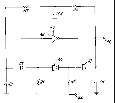
FIG. 4 is a circuit diagram of the preferred embodiment of the
invention that warps a resonant frequency of the detection oscillator
associated
with the sensor. The circuit utilizes time domain signal processing, and is
comprised of a voltage-controlled oscillator circuit in parallel with a
resonant
oscillator circuit. The voltage-controlled oscillator circuit includes sensor
18, varactor 40, reference bias capacitor C2, summing resistors R1 and R2,
phase shifting capacitors Cl and C3, and input 44. Sensor 18 has one of its
CA 02378759 2002-O1-09
WO 01/04621 PCT/US00/18793
S
terminals connected to phase shifting capacitor C3, which in turn is connected
to ground. The second terminal of sensor 18 is connected through summing
resistor R2 to input 44, and to the cathode of varactor 40. Varactor 40 is
preferably a Zetex Hyper-Hyperabrupt variable capacitance diode, type ZC932.
Varactor 40 functions as a voltage variable capacitor. Increasing the reverse
bias voltage across varactor 40 reduces its capacitance.
The anode of varactor 40 is connected through second summing
resistor R1 to ground, and to reference bias capacitor C2. Reference bias
capacitor C2 is also connected through second phase shifting capacitor C 1 to
ground.
The resonant oscillator circuit is connected in parallel with the
voltage controlled oscillator circuit. In the presently preferred embodiment,
the
resonant oscillator circuit includes inverter 42 which is also connected to
supply
+V, resistors R3 and R4, and tuning capacitor C4. Resistor R3 is connected to
the input of inverter 42, and also through capacitor C4 to ground. Resistor R4
is also connected through capacitor C4 to ground, and also in the output of
inverter 42. The input of inverter 42 is connected to the junction of
capacitors
C1 and C2, arid the output of inverter 42 is inverted to the junction of
sensor 18
and capacitor C3, and to output 46. Inverter 42 is a high gain linear
amplifier.
Voltage +V supplies the power to the resonant oscillator circuit.
Input voltage 44 provides a reverse bias do voltage to the cathode
of varactor 40. The value of the bias voltage is established by the summing
resistors R1 and R2, as well as by capacitor C2. Capacitors C1 and C3 are
phase shifting capacitors which enable startup of the circuit. The variable
reactive load of varactor 40, in series with sensor 18, forces a change in the
resonant frequency of sensor 18. The amount of the change is based on the
values of resistors R1 and R2 and the bias do voltage input at 44. Output 46
provides a signal with an adjusted resonant frequency, minus the inharmonic
tones. Output 46 is connected to a high resolution counter, such as the one
described in Application No. 08/968,081, filed November 12, 1997, for "High
Frequency Measuring Circuit" by John P. Dilger and Nile K. Dielschneider,
CA 02378759 2002-O1-09
WO 01/04621 PCT/US00/18793
6
and assigned to the same assignee as the present application. The present
invention significantly reduces the noise distortion that results in frequency
shifting, or skipping, and it significantly enhances the resolution of 18.
Under normal conditions, the sensor 18, with a nominal
S frequency of 10 MHz, typically oscillates with a maximum error of
approximately 10 Hertz (Hz). However, as noted previously, the inharmonic
mode oscillations can cause frequency skipping, thereby pulling the
fundamental frequency away from its 10 megahertz (MHz) value by as much
as 1 to 10 KHz (representing a distortion of .01 % to .1 %). Sensor 18,
however,
must have a high resolution to measure small changes in analyte
concentrations.
For example, concentrations of analyte being measured may alter the initial 10
MHz frequency of sensor 18 by about 200 Hz (representing a change of .002%).
Therefore, the frequency changes being measured as indications of change of
analyte concentrations are within the changes of distortion caused by the
inharmonic modes. Hence, the distortion must be effectively eliminated. With
appropriate establishment of values of the circuit elements shown in FIG. 4,
the
frequency warping mechanism will pull the resonant frequency of the circuit
back towards the 10 MHz fundamental value of the sensor. Thus, where
distortion might alter the fundamental frequency of the sensor by l OKHz (e.g.
to 9.990 MHz), the warping circuit will pull the initial resonant frequency of
the
circuit back to 10.0 MHz through proper selection of resistors R1 and R2 and
bias do voltage value. Hence, deviation from the initial frequency is a true
measure of analyte concentration, unaffected by noise.
The reverse bias do voltage supplied by 44 is applied with
voltage levels of l, 2.5 and 4 volts. The amount of voltage applied by 44 is
determined by the observed amount of noise distortion generated by sensor 18,
and therefore by the amount of frequency warping needed. The selected reverse
bias voltage is applied across 40 to provide a selected capacitance to
varactor
40. For example, bias do voltage levels of l, 2.5 and 4 volts affects varactor
40
to provide capacitance of 17, 9 and S picofarad (pF), respectively, in a Zetex
ZC932 diode. Typically, R1 and R2 have values of about 100 K ohms.
CA 02378759 2002-O1-09
WO 01/04621 PCT/US00/18793
Although the present invention has been described with reference
to preferred embodiments, workers skilled in the art will recognize that
changes
may be made in form and detail without departing from the spirit and scope of
the invention.