Note: Descriptions are shown in the official language in which they were submitted.
CA 02378972 2002-O1-10
WO 01/06285 PCT/DK00/00407
Hybrid Integration of Active and Passive Optical Components on a Si-Board
This invention relates to an assembly structure and a method for assembling
active and
passive photonic and/or optoelectronic devices on a silicon board. The
invention relates in
particular to an assembly structure and a method for aligning the photonic
devices during
the assembling procedure. The resulting components will be used especially for
broadband telecommunication components.
The assembly of photonic components is a very difficult and costly process.
State of the
art technology positions an optical fibre relative to a photonic component by
an active
alignment procedure. This means that during the alignment procedure the
components
are manipulated by highly accurate stages (~0.1 Nm). The incoming or outgoing
light signal
is monitored during micromanipulation until the optimum of transmitted light
has been
determined. Then the fibre is mechanically fixed employing different
techniques. The last
assembly step is to put the fibre-terminated component into a housing, which
then can be
hermetically sealed in order to protect the semiconductor component. The
housing
provides electrical as well as optical feed-throughs. The fabrication of feed-
throughs for
the optical fibre is a process, which is difficult to manufacture, too.
The assembly is of photonic components is, due to the very demanding
manufacturing
steps time consuming and makes up typically 80% of the device cost. Much could
be won
if one used planar light guiding circuits (PLCs) for broadband
telecommunication systems
not only as passive components. PLCs have a very attractive potential to
increase
functionality by directly mounting semiconductor components onto the PLC
board. But
most importantly this concept, which in the literature is referred to as
hybridisation could
also facilitate the assembly of components and the subsequent hermetic sealing
components to a high degree.
A typical application of a hybridly integrated photonic component is shown in
Fig. 1 where
a pump laser device 2 is attached onto a PLC board 10, which also hosts a
waveguide 4
leading the light from the laser to other parts of an planar lightwave circuit
(PLC). The
alignment and assembly of the semiconductor component is achieved by a simple
"clip-
CA 02378972 2002-O1-10
WO 01/06285 PCT/DK00/00407
2
on" procedure, which does not require active alignment and therefore will
greatly
decrease assembly costs.
An inherent advantage of the hybrid integration concept is that it allows the
light from the
pump laser to be coupled directly into the waveguide whereas with conventional
technologies each component has to be connected to a fibre separately, put
into a
housing and be connected using optical fibre connectors. The state-of-the art
concept
leads to bulky and difficult-to-handle components whereas the hybridisation
leads to
highly integrated and compact modules.
In the efforts to fully exploit the potential of PLCs one question is key; how
does one
obtain a long-term mechanical stability between the photonic component and the
waveguide structure on the PLC board, and how can the active alignment
procedure be
avoided? This question has created a technical challenge for the fiberoptics
components
industry. The necessary coupling tolerance is in the submicron region and the
fixation
needs a mechanical stability of less than +/- 0.1 ~m under all possible
operation- and
storage- conditions.
In the prior art there are several attempts to achieve fastening of photonic
components
such as lasers to a PLC board by passive alignment.
Methods using highly accurate Flip-Chip Bonding machines have been developed.
These
make use of optical detection of fiducials (alignment marks) on the substrate
and photonic
component. Registration and positioning are however time consuming and
equipment is
very expensive.
Self-aligned bonding which make use of micromachined V-grooves for fibre
fixation and
the surface tension forces of the molten solder material, has been proposed
and taken up
by research facilities around the world. The method has been proven to reach
the
required tolerances. Nevertheless, the needed accuracy, which is within 1 pm,
requires
extremely well controlled process tolerances on soldering and V-groove
micromachining,
which will be costly to develop.
One of the alignment concepts that make use of etched alignment structures and
surface
tension forces of the molten solder material, is presented in US 5,656,507.
Here the
CA 02378972 2002-O1-10
WO 01/06285 PCT/DK00/00407
3
silicon substrate is prepared with a waveguide, two alignment stops, a V-
shaped groove
and a trench with an L-shaped metal pad in the bottom. The bottom of the laser
holds a
ridge and an L-shaped metal pad with a solder bump so as to fit the V-shaped
groove and
the L-shaped metal pad on the silicon substrate. The principle is that when
the laser is
placed on the silicon substrate with the ridge inserted in the groove and an
edge abutted
to the alignment stops, the two L-shaped metal pads are slightly displaced
though
connected by the solder bump. When the solder is melted, it will draw the
laser into
alignment with the waveguide through surface tension forces.
Many companies have shifted their focus to alignment concepts, which require
highly
accurate pick and place machines in conjunction with alignment fiducials on
the
assembled parts (see H.L. Althaus et. al., "Microsystems and Waferprocesses
for
Volumeproduction of Highly Reliable Fibre Optic Components for Telecom and
Datacom
Applications", 47t" ECTC Conf., San Jose, CA, 1997, pp. 7-15). These concepts
are very
application specific and require large investments that only pay off for large
production
volumes. Parallel to that, an increasing number of publications emerged
proposing a
concept which makes use of dry- or wet-etched alignment structures, e.g. D. A.
Ackerman
(US 5,023,881), J. Gates et al. ("Hybrid Integrated Silicon Optical Bench
Planar
Lightguide Circuits'; 48t" ECTC Conf., Seattle, WA, 1998, pp. 551-559) and S.
A. Merrit
("A Rapid Flip-Chip Bonding Method for Semiconductor Laser Diode Arrays", 48t"
ECTC
Conf., Seattle, WA, 1998, pp. 775-779).
US 5,023,881 covers the use of pedestals which initially forms a gap in-
between the laser
and the substrate. The vertical alignment is achieved by placing the laser on
top of two
pedestals, and the precision relies on the thickness of numerous individual
layers. The
specific alignment step consists of a cold welding for tacking the laser
during the
subsequent soldering. The horizontal alignment is not addressed in this patent
and needs
to be realised presumably by micromanipulation ("in a predetermined way")
Another alignment concept, which makes use of etched alignment structures, is
presented
in US 5,721,797. The patent discloses a method for aligning a laser relative
to a fibre or a
waveguide. Here, only the method relating to the waveguide is of interest. Two
trenches
are etched into the silicon substrate to later host waveguide structure (1 St
trench) and
laser-mounting site (2"d trench). Then the second trench is filled with solder
material, the
first trench with cladding material for the optical waveguide. The procedure
ensures that
CA 02378972 2002-O1-10
WO 01/06285 PCT/DK00/00407
4
the waveguide core is at the same height as the light emitting core of the
laser waveguide
(vertical alignment). At the same time as the waveguide core material three
alignment
stops are formed to which the laser component will abut during assembly in
order to
achieve the horizontal alignment. The fabrication step is finalised by putting
the top
cladding onto the core waveguide material.
When the laser is then mounted on top of the solder (deposited into the 2"d
trench) the
component is slithered towards the three alignment structures to ensure
horizontal
alignment. It is important to note that it is the sides of the laser, which
abut the alignment
stops, and the thickness of the solder deposition, which defines the
horizontal and vertical
alignment respectively. Applying heat to the assembly, thereby melting the
solder the
laser is mechanically fixed onto the silicon substrate.
Often, hybrid integration apparatuses are not compatible with the diversity of
photonic
devices from different manufacturers. Most of the prior art implies certain
dimensions and
features of the devices in order to perform the hybrid integration (US
5,721,797). If the
design of the device is changed the assembly structure needs to be changed as
well. The
situation in a production advanced PLCs will be that that the dimensions of
photonic
devices change. It will be too expensive and time-consuming to make
adjustments to the
assembly structures.
It is a disadvantage of the existing alignment concepts (US 5,721,797) that
the accuracy
of the horizontal alignment relies on the precision etching of the alignment
structures and
on precision cleaving of the laser components. The required precision of both
technologies is in a critical range for manufacturing (<1 Nm).
It is a disadvantage of the existing alignment concepts (US 5,721,797) that
during melting
of the solder to fasten the laser onto the PLC board the surface tension
forces of the
molten solder can move the laser chip and thus destroy the horizontal and
especially the
vertical alignment.
It is a disadvantage of the existing alignment concepts (US 5,023,881 ) that
the horizontal
alignment of the components requires registration of alignment marks and
accurate and
thus costly micromanipulation to achieve the horizontal alignment.
CA 02378972 2002-O1-10
WO 01/06285 PCT/DK00/00407
It is a still further disadvantage of the existing alignment concepts (US
5,023,881 and US
5,721,797) that the vertical alignment relies on the thickness of several
individual material
layers (e.g. solder deposits) which need to be accurately deposited in
relation to the
thickness of a reference layer, which is the waveguide core of the PLC.
5
It is an object of the present invention to provide an assembly structure and
a method for
self-aligned hybrid assembly in which alignment can be realised before
fastening.
It is another object of the present invention to provide an assembly structure
and a
method for self-aligned hybrid assembly in which reworking in case of a
malfunctioning
photonic components is possible, since the malfunctioning component can be
detached
by heating the structure, and replaced by a new component.
It is still another object of the present invention to provide an assembly
structure and a
method for self-aligned hybrid assembly, which implies only a minimum of "add-
on"
features to the photonic device, and does not require certain dimensions of
the photonic
device.
It is still another object of the present invention to provide an assembly
structure and a
method for self-aligned hybrid assembly where no processing, such as etching
of the
often fragile photonic device is needed.
It is still another object of the present invention to provide an assembly
structure and a
method for self-aligned hybrid assembly where the horizontal alignment relies
on a single
mask step in a photolithographic process.
It is still another object of the present invention to provide an assembly
structure and a
method for self-aligned hybrid assembly where the vertical alignment relies on
the
positioning of aligned components on what are essentially different parts of
the same
surface.
It is still another object of the present invention to provide an assembly
structure and a
method for self-aligned hybrid assembly where no accurate cleaving is needed
since no
cleaved surfaces abut during alignment.
CA 02378972 2002-O1-10
WO 01/06285 PCT/DK00/00407
6
It is still another object of the present invention to provide an assembly
structure and a
method for self-aligned hybrid assembly of photonic components, which is
compact and
thereby easy to pack and stack.
It is still another object of the present invention to provide an assembly
structure and a
method for self-aligned hybrid assembly of an array of photonic devices on a
substrate.
It is still another object of the present invention that a hermetic sealing of
the semiconduc-
for component can be integrated into the processing, using basically the same
masks,
materials and processing steps used to form the assembly structure.
The above-mentioned objects are complied with by providing in a first aspect
of the
present invention an assembly structure comprising:
- a substrate holding a bottom cladding layer, said bottom cladding layer
comprising a first and a second part, wherein each part comprises a top and a
bottom surface separated by a distance d,
- an optical waveguide comprising a top and a bottom surface and a light
input or output end, said optical waveguide defining a first optical axis, the
bottom surface of said optical waveguide being positioned at a distance larger
than or equal to d above the bottom surface of the bottom cladding layer, and
- one or more first alignment features being formed in the second part of the
bottom cladding layer, said one or more first alignment features further
comprising a first and a second tapered side surface part in directions at
least
substantially parallel to the first optical axis.
The top surface of the first alignment features is essentially in the same
plane as the
top surface of the first part of the bottom-cladding layer. In order to
confine light
within the optical waveguide an additional material is provided to embed the
waveguide core.
CA 02378972 2002-O1-10
WO 01/06285 PCT/DK00/00407
7
The assembly may further comprise a set of electrical contact pads suitable
for
providing electric energy to an optoelectronic device such as a semiconductor
laser, a
light emitting diode (LED) or a photodiode.
Preferably, the bottom surface of the optical waveguide core is positioned on
the top
surface of the bottom cladding layer at a distance substantially equal to d,
where d is
measured from the bottom surface of the bottom cladding layer.
The assembly structure according to the first aspect of the present invention
may
further comprise
- an optoelectronic device comprising an active part and a light input or
output
port, said input or output port being optically aligned with the waveguide
output or input end by having the optoelectronic device arranged on top of the
first alignment features to thereby obtain vertical alignment.
By arranging the optoelectronic device on top of the alignment features, a
vertical
alignment is achieved between the active part of the device and the waveguide.
However, the active part of the device may be positioned at a given height
above the
bottom surface of the device, whereby the light input or output port will be
positioned at a given height over the bottom-cladding layer when the device is
arranged on top of the alignment features. Depending on this given height, and
upon
the respective sizes of the input/output port and the waveguide end, the
waveguide
may be positioned at a distance d+x above the bottom surface of the bottom
cladding layer, where x compares to the given height of the active part in the
optoelectronic device. The distance x may be controlled by depositing one or
more
material layers between the bottom-cladding layer and the waveguide core.
In order to horizontally align the light receiving input end of the optical
waveguide
with the light output port of the optoelectronic device, the assembly
structure may
further comprise one or more second alignment features abutting the one or
more of
the first alignment features of the second part of the bottom cladding layer.
Preferably, the second alignment features abut the first and second tapered
side
CA 02378972 2002-O1-10
WO 01/06285 PCT/DK00/00407
8
surface parts of the first alignment features whereby the horizontal alignment
is
performed in the direction transversely to the optical axis of the waveguide.
The tapered surface parts provide an improved horizontal alignment on several
points. The abutting of the second alignment features to the tapered side
surface
parts wedges the optoelectronic device to the structure and thereby provides a
steady fixation until the devices is properly secured. Moreover, the
orientation of the
tapered side surface parts improves the accuracy in the critical positioning
parameters of the optoelectronic device in relation to the waveguide. In the
horizontal
alignment, the direction transversely to the optical axis of the waveguide is
very
critical in order for light to couple between the waveguide and the active
region.
However, the distance between waveguide and the active region along the
optical axis is
considerably less critical. By providing a tapering in a direction at least
substantially
parallel to the first optical axis, the inherent inaccuracy of the position
and shape of
the first and second alignment features primarily affects the less critical
distance
between the waveguide and the active region.
For example, the optoelectronic device may be a light source comprising a
light
output port, an active part and one or more second alignment features being
adapted
to abut one or more of the first alignment features of the second part of the
bottom
cladding layer so as to align the light receiving input end of the optical
waveguide
with the light output port of the light source.
Etching may be applied to fabricate the assembly structure. In order to
control the
etching process an etch stop layer may be provided at some stage during the
fabrication process on top of the first alignment features. In an embodiment
according to the invention the etch stop layer is maintained on top of the
first
alignment features thereby arranged below the optoelectronic device.
It is preferred that during the formation of the assembly structure, the
positioning of
the optical waveguide and the first alignment features is defined using a
single mask.
The reason for this being that for every mask being involved in the
fabrication
process an uncertainty is introduced in the positioning of one mask relative
to
another mask.
CA 02378972 2002-O1-10
WO 01/06285 PCT/DK00/00407
9
The second alignment features may comprise solder stripes arranged on the
bottom
of the optoelectronic device so as to at least partly engage the side walls of
the first
alignment features. Preferably, at least two solder stripes are arranged on
the bottom
of the optoelectronic device. In order to provide electrical power to the
optoelectronic
device the optoelectronic device may be soldered to metallized contact pads
formed
on exposed parts of the substrate.
As long as the solder stripes are positioned symmetrically, any inaccuracy in
their
separation or size will change the gap between the optoelectronic device and
the
waveguide, but not result in transverse misalignment. This means that if there
is a
tolerance in the width of the symmetrically designed 2 solder stripes the
horizontal
alignment will be unaffected whereas the less critical distance between
waveguide and
optoelectronic device will be changed according to the taper angle.
Preferably, two of the first alignment features provides the first and second
tapered
side surface parts on outer side surfaces, and the alignment features may be
separated by a distance larger than the width of the active part of the
optoelectronic
device.
As already mentioned, the optoelectronic device may comprise a variety of
light
sources, such as a semiconductor laser or a diode.
In a second aspect, the present invention relates to a method of forming an
assembly
structure for assembling an optoelectronic device and an optical waveguide,
said
optical waveguide comprising a light input end for receiving light emitted
from an
output port of the optoelectronic device, said method comprising the steps of:
- providing a bottom cladding layer on top of a substrate, said bottom
cladding
layer comprising a first and a second part, wherein each part comprises a top
and a bottom surface separated by a distance d,
- providing a core layer on top of at least part of the bottom cladding layer,
CA 02378972 2002-O1-10
WO 01/06285 PCT/DK00/00407
- forming the optical waveguide in the core layer, said optical waveguide
thereby extending along a first optical axis in a plane and at a distance
larger
than or equal to d from the bottom surface of the first part of the bottom
cladding layer, and
5
- forming one or more first alignment features in the second part of the
bottom cladding layer so that at least one top surface of the first alignment
features is in essentially the same plane as the top surface of the first part
of
the bottom cladding layer, the step of forming the one or more first alignment
10 features comprises the step of forming a first and a second tapered side
surface part in directions at least substantially parallel to the first
optical axis.
The method according to the second aspect of the present invention may further
comprise the step of:
aligning the output port of the optoelectronic device with the light input end
of optical waveguide, said alignment comprising the step of arranging the
optoelectronic device on top of the one or more alignment features so as to
obtain vertical alignment.
The optical waveguide may extend on the top surface of the bottom-cladding
layer at
a distance substantially equal to d above the bottom surface of the bottom-
cladding
layer.
As mentioned in relation with the first aspect of the present invention the
optoelectronic device may further comprise one or more second alignment
features
abutting the first and second tapered side surface parts of the first
alignment
features so as to horizontally align the light receiving input end of the
optical
waveguide with the light output port of the optoelectronic device. By
providing the
tapering in a direction at least substantially parallel to the first optical
axis, the
inherent inaccuracy of the position and shape of the first and second
alignment
features primarily affects the less critical distance between waveguide and
the active
region. Again, it is preferred that the positioning of the optical waveguide
and the
first alignment features are defined using a single mask.
CA 02378972 2002-O1-10
WO 01/06285 PCT/DK00/00407
11
The method according to the second aspect of the present invention may even
further comprise the step of providing an etch stop layer on at least part of
the
second part of the bottom cladding layer prior to deposition of the core
layer, said
core layer extending on both the first and the second part of the bottom
cladding
layer thereby covering at least part of the etch stop layer.
The formation of the optical waveguide and the first alignment features
preferably
comprises the steps of:
a) defining the horizontal configuration of the optical waveguide and the
first
alignment features in the core layer by a single mask process,
b) partially removing the core layer thereby forming the optical waveguide and
defining the first alignment features in the core layer,
c) removing that part of the etch stop layer not being covered by the core
layer,
d) providing a top cladding layer so as to at least partly cover the optical
waveguide and optionally the one or more alignment features formed in the
core layer, and
e) removing the top-cladding layer, the core layer and at least part of the
second part of the bottom cladding layer to thereby form the first alignment
features in the bottom-cladding layer.
The etch stop layer defining the one or more alignment features formed in the
bottom
cladding layer may optionally be totally removed or only partly removed. If
the etch
stop layer is only partly removed the remaining layer may be used to adjust
the
height of the optoelectronic device relative to the optical waveguide.
The removing in step e) may comprise etching the second part of the bottom
cladding layer so as to expose that part of the substrate not being covered by
the
CA 02378972 2002-O1-10
WO 01/06285 PCT/DK00/00407
12
first alignment features. Preferably, the etching process involves an
anisotropic etch,
such as reactive ion etching.
Preferably, the first alignment features comprises two alignment features
having
outwardly tapered side surface parts, said two alignment features being
separated by
a distance larger than or equal to the width of the active part of the
optoelectronic
device. The one or more second alignment features are arranged on the bottom
of
the optoelectronic device so as to at least partly engage the outer side walls
of the
first alignment features while aligning the optoelectronic device. The second
alignment features may comprise solder stripes so as to electrically connect
the
optoelectronic device to e.g. a power supply. Preferably, at least two solder
stripes
are arranged on the bottom of the optoelectronic device.
The method according to the second aspect of the present invention may further
comprise soldering the optoelectronic device to one or more electrical contact
pads
formed beside the alignment features on exposed parts of the substrate.
Preferably,
soldering is performed by applying heating the solder stripes above a certain
melting
temperature. If e.g. a bad connection has been established during soldering,
or the
optoelectronic device turns out to be malfunctioning, the device may be
removed by
heating the assembly and thereafter replaced with new device.
The optoelectronic device may comprise any kind of light source, such as a
laser
diode or an LED. The laser diode may be a semiconductor laser diode.
In a third aspect, the present invention relates to an assembly structure
comprising:
- a substrate having one or more first alignment features disposed thereon,
and
- a first photonic device having a light input or output port for receiving or
emitting
light along a first optical axis, and having a bottom surface having one or
more
second alignment features disposed thereon,
the assembly structure being characterised in that:
CA 02378972 2002-O1-10
WO 01/06285 PCT/DK00/00407
13
the one or more first or second alignment features forms a first and a second
side
surface part which are tapered in directions at least substantially parallel
to the first
optical axis, and
the first photonic device is positioned on top of at least one of the one or
more first
alignment features, whereby two or more surface parts of the one or more first
alignment features abuts two or more surface parts of the one or more second
alignment features, the abutting surface parts comprising the first and second
side
surface parts.
As in the case of the first aspect, providing a tapering in a direction at
least substantially
parallel to the first optical axis, the inherent inaccuracy of the position
and shape of
the first and second alignment features primarily affects the less critical
positioning
along the first optical axis.
The assembly structure according to the third aspect of the present invention
may
further comprise:
- a second photonic device comprising a light input or output port for
receiving or
emitting light along a second optical axis, and comprising a bottom surface
having one or more second alignment features disposed thereon, wherein
the one or more first or second alignment features provides a third and fourth
side
surface part which are tapered in directions at least substantially parallel
to the
second optical axis, and
the second photonic device is positioned on top of at least one of the one or
more
first alignment features, whereby two or more surface parts of the one or more
first
alignment features abuts two or more surface parts of the one or more second
alignment features, the abutting surface parts comprising the third and fourth
side
surface parts.
The light input or output port of the first and/or second photonic device may
have a
predetermined orientation and height with respect to the substrate. This
predeter-
CA 02378972 2002-O1-10
WO 01/06285 PCT/DK00/00407
14
mined orientation and height determines the optical axis along which the
photonic
device may receive or emit light. In most cases, a photonic device does not
define
one unique optical axis since it may receive or emit light propagating along a
small
range of directions such as directions within a cone radiating from the input
or output
port. Hence in such cases the first optical axis may be defined as the centre
axis of
such a cone. Alternatively, the optical axis may be defined by other features
of the
assembly structure such as another input or output port coupling light to/from
the
photonic device.
In one example, the first photonic device comprises a light input port and the
second
photonic device comprises a light output port. The photonic devices are
positioned so
as to align the light input port of the first photonic device with the light
output port
of the second photonic device. This example could be the situation where a
light
source, such as a semiconductor laser or an LED, is aligned with a light
receiving
input end of an optical waveguide, such as an optical fibre or a planar
waveguide, so
as to couple electromagnetic radiation from the optoelectronic device to the
optical
waveguide. In this case the first optical axis may be defined as the straight
line
between the output and the input ports.
In another example, the first photonic device and the second photonic device
both
have a light output port, and the photonic devices are positioned so as to
align the
two light output ports along two parallel optical axes. This example could be
the
situation where two semiconductor laser diodes, are to be aligned relative to
each
other so as to e.g. emit two substantially parallel beams of electromagnetic
radiation.
The second alignment features of the first and/or second photonic device may
comprise one or more solder stripes. Preferably, at least two solder stripes
are
arranged on the bottom of a photonic device.
A photonic device may comprise an active waveguide component, such as an
optical
amplifier, such as a fibre amplifier.
In a fourth aspect, the present invention relates to a method of forming an
assembly
structure, said method comprising the steps of:
CA 02378972 2002-O1-10
WO 01/06285 PCT/DK00/00407
- providing a substrate having one or more first alignment features disposed
thereon,
5 - providing a first photonic device having a light input or output port for
receiving
or emitting light along a first optical axis, and having a bottom surface
having one
or more second alignment features disposed thereon, wherein
the one or more first or second alignment features forms a first and a second
side
10 surface part which are tapered in directions at least substantially
parallel to the first
optical axis,
the method further comprising the step of:
15 - positioning the first photonic device on top of at least one of the one
or more first
alignment features, whereby two or more surface parts of the one or more first
alignment features abuts two or more surface parts of the one or more second
alignment features, the abutting surface parts comprising the first and second
side surface parts.
Again, providing a tapering in a direction at least substantially parallel to
the first
optical axis, the inherent inaccuracy of the position and shape of the first
and second
alignment features primarily affects the less critical positioning along the
first optical
axis. Either of the first or second alignment features held by the substrate
or by the
photonic device may comprise the tapered side surface parts. Optionally, both
the
first and second alignment features are tapered.
The method may further comprise the steps of:
- providing a second photonic device comprising a light input or output port
for
receiving or emitting light along a second optical axis, and comprising a
bottom
surface having one or more second alignment features disposed thereon, wherein
CA 02378972 2002-O1-10
WO 01/06285 PCT/DK00/00407
16
the one or more first or second alignment features provides a third and fourth
side
surface part which are tapered in directions at least substantially parallel
to the
second optical axis, and
- positioning the second photonic device on top of at least one of the one or
more
first alignment features, whereby two or more surface parts of the one or more
first alignment features abuts two or more surface parts of the one or more
second alignment features, the abutting surface parts comprising the third and
fourth side surface parts.
For most applications the light input or output port of a photonic device has
a
predetermined orientation and height with respect to the substrate. This
predeter-
mined orientation and height determines the optical axis along which the
photonic
device may receive or emit light
Different schemes may arise. The first photonic device may have a light input
port
whereas the second photonic device may have a light output port. The situation
may
also be that the first photonic device and the second photonic device may both
have
a light output port. In both cases the first and second photonic devices are
positioned
relative to each other so as to align the input/outputs so that
electromagnetic
radiation propagates substantially along at least one predetermined optical
axis.
Preferably, the height of the first alignment features may be adjusted so as
to obtain
vertical alignment. The engagement of the first alignment features and the
second
alignment features ensures horizontal alignment. Thus both vertical and
horizontal
alignment can be achieved prior to fixation of a photonic device.
Preferably, it is the first alignment features, held by the substrate, which
provides the
tapered side surface parts. In order to provide aligned of the first and
second
photonic device, the first alignment features providing the first to fourth
tapered side
surface parts are formed in a single mask step. The second alignment features
of the
first and/or second photonic device may comprise one or more solder stripes.
Preferably, at least two solder stripes are arranged on the bottom of each
photonic
device.
CA 02378972 2002-O1-10
WO 01/06285 PCT/DK00/00407
17
A photonic device may comprise a passive optical component, such as an optical
waveguide, such as an optical fibre or a planar waveguide. A photonic device
may
also comprise an optoelectronic device, such as a laser diode or an LED.
Finally, a
photonic device may comprise an active waveguide component, such as an optical
amplifier. In order to achieve amplification, the active waveguide may
comprise rare-
earth materials, such as erbium.
In yet another aspect, the invention relates to an assembled structure
comprising a
first, lower structure part and a second, upper structure part, wherein:
- the first structure part comprises:
- a first substrate, an upper surface of which defines a first plane, the
substrate
comprising a first and a second part
- a first radiation guiding, emitting, and/or receiving means positioned on or
above the first part of the first substrate and in a fixed relation thereto,
the
means defining a first optical axis extending at least substantially parallel
to
the first plane,
- one or more first alignment elements positioned on or above the second part
of the first substrate, the one or more first alignment elements having one or
more upper surface parts being in a fixed relationship to the first optical
axis
and the first plane, and the one or more first alignment elements having one
or more side surface parts being positioned in a predefined position in
relation
to the first optical axis,
- the second structure part comprises:
- a second substrate having a lower surface defining a second plane being at
least substantially parallel to the first plane,
- a second means for guiding, emitting, and/or receiving radiation, the means
defining a second optical axis and being positioned below the second
substrate and in a fixed relation thereto,
CA 02378972 2002-O1-10
WO 01/06285 PCT/DK00/00407
18
- one or more second alignment elements positioned below the second
substrate, and the one or more second alignment elements having one or more
side surface parts being positioned in a predefined position in relation to
the
second optical axis,
the second structure part having one or more lower surface parts being in a
fixed
relationship to the second optical axis and the second plane,
the one or more first and second alignment elements being relatively
positioned so
that, when the first and second optical axes are at least substantially
coincident:
- at least part of the one or more upper surface parts of the one or more
first
alignment elements abut at least part of the one or more lower surface parts
of
the second structure part,
- at least part of the one or more side surface parts of the one or more first
alignment elements abut at least part of the one or more side surface parts of
the
one or more second alignment elements, and
- the abutting side surface parts of at least one of the one or more first and
second
alignment elements comprising at least two surface parts extending in
different
planes, at angles different from 0 and 90 degrees from the first optical axis.
This has the advantage that the abutting side surface parts and upper and
lower
surface parts may be positioned so as to, when projected perpendicularly onto
the
first plane, reside within an area within the first plane, the area being
defined as the
overlap between the first and second parts when these are projected
perpendicularly
onto the first plane. Thus, all engaging parts or surfaces may not comprise
any parts
of those edges of the structure part created by separation following a mass
manufacturing of such structure parts.
Normally, a large number of such structure parts are prepared in the same
process
and on the same wafer. Separation is performed subsequently by simply cutting
or
breaking the wafer with the structure part. Such separation will normally not
result in
edges which have well defined positions and distances in relation to e.g one
or more
light guides or the like in the structure parts.
CA 02378972 2002-O1-10
WO 01/06285 PCT/DK00/00407
19
As mentioned above, it may be desired that the first and second parts each
further
comprises a set of electrical contact pads positioned so as to abut or engage
and
thereby provide electrical contact between the contact pads of the first and
second
parts.
In a preferred embodiment, the second alignment elements comprise at least
one,
such as at least two, solder stripes, and the first structure element
comprises at least
one contact pad positioned so as to abut or engage the at least one solder
stripe of
the second part. In this situation, the first and second structure parts may
be fixedly
interconnected at least in part by an engagement, such as a soldering, between
the
solder stripes) and contact pad(s).
Naturally, the overall positioning and fastening of the two structure parts
entails no
demands as to the function or operation of the two radiation guiding,
emitting, and/or
receiving means of the two structure parts. Thus, the radiation guiding,
emitting,
and/or receiving means of at least one of the first and second structure parts
may,
e.g., comprise:
- a waveguide, such as an optical fibre or a planar waveguide, where the
optical
axis is defined by a longitudinal axis of the waveguide,
- a light emitter, such as a semiconductor laser diode or an LED, and where
the
optical axis is defined as an axis of symmetry of radiation emitted by the
light
emitter, and/or
- an active waveguide component, such as an optical amplifier, such as a fibre
amplifier, where the optical axis is defined by a longitudinal axis of the
waveguide.
One of the advantages of the present assembly may be seen, as, in the first
structure
part, the one or more upper surface parts may define a plane at least
substantially
comprising a lower side of the first means for guiding, emitting and/or
receiving
radiation. This provides the advantage, as mentioned above, that the inter-
positioning
thereof may be obtained with a good precision.
CA 02378972 2002-O1-10
WO 01/06285 PCT/DK00/00407
In order to obtain a precise and reproducible positioning of the structure
parts, the
abutting side surface parts of one of the first and the second structure part
preferably define an outwardly tapered part, viewed from the respective means
for
guiding, emitting, and/or receiving radiation and wherein the abutting side
surface
5 parts of the other of the first and the second structure part preferably
define an
inwardly tapered part, viewed from the respective means for guiding, emitting,
and/or
receiving radiation. In this manner, the two tapered parts may be adapted to
fit in a
manner so that a quick and error-free connection is obtained.
10 In that situation, it is preferred that, in one or both of the first and
second structure
part, the one or more alignment elements are positioned so as to provide a
space at
least corresponding to a cross section of an active part of the means for
guiding,
emitting, and/or receiving radiation, the cross section being translated along
the
respective optical axis over the second part of the respective structure part.
In that
15 manner, radiation guiding, emitting, and/or receiving means having such
dimensions
may be positioned in that space in order to optically fit the other radiation
guiding,
emitting, and/or receiving means.
In yet another aspect, the invention relates to a first and/or a second
structure part
20 for use in the assembled structure.
Also, an aspect of the invention relates to a method of manufacturing a first
structure part for use in the assembled structure, the method comprising:
1 . providing a substrate having a first and a second part,
2. providing a means for guiding, emitting, and/or receiving light, the means
defining
an optical axis, the means being positioned on or above the first part of the
substrate and so as to be fixed in relation to the substrate and so that the
optical
axis is in a predetermined relation to the substrate,
3. providing one or more alignment elements on or above the substrate, the one
or
more alignment elements being positioned:
- on or above the second part of the substrate,
- so that the one or more alignment element has/have one or more upper
surface parts being in a fixed relationship to the first optical axis and the
first
plane, and
CA 02378972 2002-O1-10
WO 01/06285 PCT/DK00/00407
21
- so that the one or more first alignment element has/have one or more side
surface parts being positioned in a predefined position in relation to the
first
optical axis.
Preferably, steps 2) and 3) comprise the steps of:
I. providing a first layer of a first material on or over at least
substantially all of
an upper surface of the first and second parts of the substrate, the first
material having a first effective refractive index,
II. providing a second layer of a second material on at least substantially
all of an
upper surface of the first layer and at least over or at the first part of the
substrate, the second material having a second effective refractive index
being different from the first effective refractive index, and
III. removing a predetermined part of the second layer.
Advantageously, steps 2) comprises providing between steps I) and II), a third
layer
of a third material on the upper surface of the first layer and at least over
or at the
second part of the substrate. Preferably, the third material are adapted to
withstand a
process of removing at least part of the first layer.
Also, it is desired that:
- step II) comprises providing the second layer also on the third layer,
- step III) comprises the steps:
a) predefining the parts, both over or at the first and second parts of the
substrate, of the second layer which should be removed,
b) removing the predefined parts of the second layer.
In that situation, step 2) may comprise providing, at least over or at the
first part of
the substrate, a fourth layer of a fourth material on the structure resulting
after step
b), the fourth material having a refractive index being different from the
second
refractive index.
Step III) may further comprises removing those parts of the third layer on
which
predefined parts of the second layer are positioned.
CA 02378972 2002-O1-10
WO 01/06285 PCT/DK00/00407
22
In that situation, step 3) preferably further comprises removing all remaining
parts of
the second layer on or above the second part of the substrate.
Also, step 2) preferably further comprises removing at least substantially all
parts of
the first layer, which parts correspond to parts of the third layer removed
during step
b).
Preferably, step III) further comprises removing at least substantially all
remaining
parts of the third layer above or at the second part of the substrate.
A major advantage of the invention is that step a) may comprise predefining
the parts
in a single step. Naturally, this may be obtained using virtually any
technique.
However, at present, it is preferred to use a lithographic process and by
using a
single mask.
It is also preferred that the further removing step of step 3) is performed
using a
predefined removal procedure, such as an etching procedure, such as reactive
ion
etching, and wherein step II) comprises providing a third layer of a third
material,
such as an etch stop, which is adapted to not be removed during the predefined
removal step.
Yet another aspect of the invention relates to a method of assembling an
assembled
structure according to claim 1, the method comprising:
- providing the first and second structural parts, then
- positioning the first and second structural parts in order to form the
assembly,
and finally
- fixing the first and second structural parts to each other.
This firstly positioning and then fixing the parts has a number of obvious
advantages,
e.g. that proper functioning of each part can be checked before fixing which
may be
an irreversible process.
In the following, the present invention will be described in further detail
with references to
the figures listed below.
CA 02378972 2002-O1-10
WO 01/06285 PCT/DK00/00407
23
Fig. 1 shows typically optical chip including a hybrid integrated pump laser
and a
waveguide.
Fig. 2 shows the first step of fabricating the assembly structure, in which a
bottom
cladding is deposited on a silicon substrate.
Fig. 3 shows a polysilicon etch stop applied on part of the bottom cladding.
Fig. 4 shows a layer of core glass applied on the structure of Fig. 3.
Fig. 5 shows the structure of Fig. 4 after an etching step defining the
waveguide and
alignment taper templates.
Fig. 6 shows the structure of Fig. 5 after removal of the accessible
polysilicon etch stop.
Fig. 7 shows several top cladding layers applied on the structure of Fig. 6.
Fig. 8 shows the structure of Fig. 7 after removal by etching of the front
part of the top
cladding and alignment taper templates.
Fig. 9 shows continued etching of the structure of Fig. 8 completing the
alignment tapers.
Fig. 10 shows metal pads serving as laser electrodes and thermal paths applied
on the
structure of Fig. 9.
Fig. 11 shows a photonic device to be applied on top of the structure of Fig.
10.
Fig. 12 shows the aligned assembled structure while melting the solder stripes
for
fastening.
Fig. 13 shows an exploded view of the structure of Fig. 12 revealing the
melted solder
stripes.
Fig. 14 is a front view of the aligned assembled structure.
CA 02378972 2002-O1-10
WO 01/06285 PCT/DK00/00407
24
Fig. 15 is a close up on Fig. 14 showing the solder stripes, the alignment
tapers and the
metal pads.
Fig. 16 shows the same as Fig. 15 after melting the solder stripes.
Fig. 17 A and B shows arrays of alignment tapers with photonic devices.
Fig. 18 shows an array of alignment tapers with photonic devices on a
substrate also
holding other features.
Fig. 19 shows an alternative embodiment of the tapered alignment features of
the present
invention.
Fig. 20A and B are top and cross sectional views of how an efficient sealing
may be
provided to an assembly structure according to the present invention.
The fabrication of the structures to be applied in hybrid integration
procedures according
to the present invention makes use of standard semiconductor technology. The
invention
can be realised in a plurality of embodiments of which only a representative
selection is
described here.
In a first embodiment the present invention relates to an assembly structure
for performing
hybridisation of an opto-electronic device onto a substrate holding a
waveguide. An opto-
electronic device can be a light emitting component such as a laser or a Light
Emitting
Diode (LED), or a light receiving component such as a photodiode. The hybrid
integration
includes aligning the laser and the waveguide, and soldering the laser to the
substrate
securing a long term mechanical stability.
The description of this first embodiment also serves as a general description
of the
essential features involved in the present invention. Therefore not all steps
and features
included in this description are necessary in order for the invention to be
realised, and the
description should by no means be interpreted as limiting the scope of the
invention. The
composition of the assembly structure is best described by going through the
stepwise
manufacturing procedure with reference to Figures 2-13.
CA 02378972 2002-O1-10
WO 01/06285 PCT/DK00/00407
Fig. 2 shows the first step of fabricating the assembly structure, in which a
bottom
cladding layer 12 is deposited on a substrate 10. Preferably the substrate is
composed of
Silicon or other inorganic or organic substrate material; the bottom-cladding
layer is SiOz
5 or other materials different from the core material to be deposited later.
For practical
purposes, the shown structure is nominally divided into a first part (in the
back) and a
second part (front). Fig. 3, an etch stop 14 is deposited on the second part
of the bottom
cladding. Possible etch stop materials are polysilicon, Boron doped
polysilicon, metals or
other inorganic materials. The next step consists of covering the structure
with a
10 deposited layer 16 of core glass, typically Germanium doped Si02 or other
materials
different from the cladding material, as shown in Fig. 4.
The depositing of cladding, etch stop and core glass layers can be carried out
using
Plasma Enhanced Chemical Vapour Deposition (PECVD), Low Pressure Chemical
15 Vapour Deposition (LPCVD), or some vacuum deposition technique.
In Fig. 5, the formation of the waveguide core and alignment taper templates
is carried out
by a photolithographic process. First, the core glass layer is deposited onto
the Si wafer.
Next, the waveguide core and alignment taper templates are defined in the
resist in the
20 same photoresist processing step. The following RIE process removes the
surrounding
core glass material, leaving only the waveguide core 18 and the alignment
taper
templates 19. It is in this step that the essential horizontal alignment takes
place. Since
the waveguide core and the alignment taper templates are defined
simultaneously in one
mask step, the precision of the horizontal alignment is very precisely
defined.
When working with optics in general, one often takes precautions to avoid back-
scattering
from surfaces such as input/output facets. The photolithography mask step
described
above provides a simple measure for doing this in the present invention. By
changing the
illumination mask, the end of the waveguide core can be defined having an
angled
termination, hence any reflection from this surface will leave the system.
The polysilicon etch stop 14 not covered by the alignment taper templates are
removed by
wet- or dry etching, exposing the bottom cladding layer, see Fig. 6. The
waveguide core
has to be covered by a material for it to be able to guide electromagnetic
radiation. There
exist several choices of materials for embedding the waveguide core for it to
be able to
CA 02378972 2002-O1-10
WO 01/06285 PCT/DK00/00407
26
guide electromagnetic radiation. These can be defined using parameters such as
refractive index. This is done in Fig. 7 where a top cladding layer 13,
preferably similar to
the bottom cladding layer, is deposited on the structure of Fig. 6. This
cladding layer is
removed again in an RIE process, but only from the second part of the
structure, resulting
in the structure in Fig. 8.
Completion of the etching process in Fig. 9 forms the alignment tapers 20 in
the bottom
cladding 12. Going from fig. 8 to 9, the etch stop mask 15 is also removed,
revealing the
top surface of the alignment tapers. It is important to note that the top
surface of the
bottom cladding layer 12 forms both the top surface of the alignment tapers
and the
surface on which the waveguide core 18 is deposited, that is, these are in the
same plane.
Thereby a very precise vertical alignment can be achieved by placing the
object to be
aligned on top of the alignment tapers.
A number of metal pads 22 are deposited on the exposed part of the silicon
substrate 10
next to the alignment tapers 20 as shown in Fig. 10. These metal pads serve as
wetable
regions for binding solder to the substrate in a later soldering (see e.g. Fig
16). After this
soldering, the pads also serve as both thermal paths to the silicon substrate,
and as
electrical contacts for the opto-electronic device. The depositing of the
metals can be
carried out by electroplating or vacuum deposition techniques.
As can be seen from Fig. 10, the whole assembly structure 30 is deposited on
the
substrate 10, and therefore no etching of trenches and groves in the silicon
wafer is
needed.
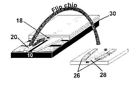
Referring now to Fig. 11, the opto-electronic device 24, a semiconductor laser
in the
preferred embodiment, is presented upside down showing the active region 28 to
be
aligned with the waveguide. The active region preferably resides so as to have
its optical
axis elevated above the bottom surface of the laser a distance equal to the
distance of the
optical axis of the waveguide above the bottom cladding layer. The exact
position of the
active region will be commented on later.
The laser 24 also holds one or more alignment features, here in the form of
one or more
solder stripes 26, which are deposited symmetrically on the bottom surface of
the laser,
with the active region 28 in the centre. One alignment step with the active
region of the
CA 02378972 2002-O1-10
WO 01/06285 PCT/DK00/00407
27
laser as reference will be needed in depositing the solder stripes, the
accuracy of which is
typically 0.2Nm. Electroplated stripes of AuSn80 having very smooth surface
structures is
the preferable solder material in the present invention. Semiconductor lasers
are often
fragile and need a very gentle handling. Since the solder stripes are "add-on"
there is no
need for etching the laser, which is considered a major advantage.
To perform the alignment, the laser 24 is flipped according to the arrow in
Fig. 11, for the
solder stripes 26 to fit the alignment tapers 20. Thereafter the laser is slid
towards the first
part of the assembly structure, until the solder stripes abut the alignment
tapers, as is
achieved in Fig. 12. This last action is where the alignment with the
waveguide takes
place and the tapering of the alignment tapers 20 guides or interlocks the
laser 24 so that
the active region 28 is aligned with the waveguide core 18. The laser now
rests upon the
alignment tapers which ensures the vertical alignment (note the vertical
position of the
active region described above), and the solder stripes clamps the alignment
tapers
ensuring the horizontal alignment. Thus both vertical and horizontal alignment
has been
achieved, and due to the clamping of the solder stripes to the alignment
tapers, they are
held together firmly without being inseparable.
The horizontal alignment is only sensitive to the relative alignment of the
solder stripes 26
to the active region 28. As long as the solder stripes are positioned
symmetrically, any
amendments of their separation will change the gap between the laser and the
waveguide, but not result in lateral misalignment. In Fig. 12, the aligned and
assembled
structure is shown while melting the solder stripes for fastening the opto-
electronic device.
Fig. 13 shows an exploded view of the structure of Fig. 12 revealing the
melted solder
stripes.
The alignment and fastening procedure performed in Figures 11 to 13 are
described in
detail referring to Figures 14 to 16. Figure 14 shows a front view of Fig. 12
where it is
seen that the solder stripes 26 position the active region 28 precisely
between the
alignment tapers 20. From the close-up in Fig. 15 it is seen that the solder
stripes
contributes solely to the horizontal alignment, and therefore the height of
the solder
stripes is only restricted by the height of the alignment tapers. It is with
noting that the
alignment is performed prior to fastening of the opto-electronic device, hence
any errors
or inaccuracies obstructing a perfect alignment can be detected, and the
fastening
rejected.
CA 02378972 2002-O1-10
WO 01/06285 PCT/DK00/00407
28
After alignment, the melting of the solder stripes 26 effected from Fig. 15 to
16 is carried
out by heating the assembled structure. In Fig. 16, the solder bulges up,
wets, and excess
solder flows along the metal pads 22 to make both thermal and electrical
contact to the
silicon substrate 10. This contact enables power supply to the laser 24 and
enhances its
temperature stability since it is over a broad area. Making additional wire
bonding to the
laser will heat the assembly considerably, however, since the laser rests on
top of the
alignment tapers, softening of the solder does not present a problem.
In the description of the assembly structure above (Fig. 11 ), it was implied
that the active
region 28 was residing a certain height above the bottom surface of the laser
24.
However, in specific opto-electronic devices, the region to be aligned with
the waveguide
resides some given height above the bottom surface, inside the device, not
being equal to
the height of the centre of the waveguide core. This will cause the region 28
to be either
elevated or lowered relative to the waveguide centre, when the device is
mounted.
Two embodiments of the present invention addresses this problem, a first
applies where
the active region is elevated relative to the waveguide core centre, and a
second when it
is lowered.
First embodiment: The waveguide core 18 can be elevated by depositing a second
cladding layer prior to formation of the core layer (16 in Fig. 4) by vacuum
deposition.
Instead of resting on the top surface of the bottom cladding layer, the
waveguide core 18
in Fig 5 now rests on the remaining part of the second cladding layer, resting
on the
bottom cladding layer 12. This will elevate the waveguide a distance equal to
the
thickness of the second cladding layer above the top surface of the bottom
cladding layer.
Referring now to Figure 9, the top surface of the alignment taper 20 will
still be in the
plane of the top surface of the bottom cladding layer 12. Since the thickness
of the second
cladding layer is known, the top surface of the alignment tapers 20 is still
well defined
relative to the waveguide.
Second embodiment: The mounted device can be elevated relative to the
waveguide by
increasing the height of the alignment tapers. This is easily done by leaving
all or part of
the etch stop mask 15 in Fig. 8 otherwise removed after the etching of the
cladding layers.
CA 02378972 2002-O1-10
WO 01/06285 PCT/DK00/00407
29
Adjusting the original thickness of the etch stop layer allows the mounted
device to be
elevated a given height relative to the waveguide.
These two well-defined height adjustments using only the thickness of a single
layer,
permits a precise vertical alignment of the waveguide and the opto-electronic
device, also
when the region to be aligned resides some given height above the bottom
surface, i.e.
inside the opto-electronic device.
Alternative embodiments of the present invention exist when the object is to
align several
photonic devices either relative to each other, or relative to another object.
Here, a
photonic device refers to both opto-electronic components and other optical
devices such
as amplifying waveguides. In this case there may not be a waveguide in the
assembly
structure. The alignment tapers will be positioned in either of two ways, as
described in
Figures 17 and 18:
1. a number of alignment tapers 20 defined in one mask step, and formed in the
same
cladding layer with the top surfaces of all tapers being in the same plane
(Fig. 17 A
and B), or
2. a number of alignment tapers 20 defined and formed as in 1, but the one
mask step
including the definition of another feature 32 on the substrate (Fig. 18).
This other
feature could be a photonic device or another alignment feature.
The embodiment addressed in Fig 17A applies where two or more photonic devices
are
hybrid integrated after each other in a line. Contrary to the waveguide in the
assembly
structure described above, none of the photonic devices to be aligned are
formed on the
substrate. The two or more photonic devices 25 have light input/output ports,
which are to
be internally aligned in order to acquire an efficient light coupling between
them.
In the embodiments shown in Figures 17B and 18 the alignment tapers and the
attached
device(s), are oriented relative to an imaginary frame of reference. The
alignment will be
both an alignment and a three-dimensional positioning with a high precision in
especially
the transverse directions relative to the alignment tapers.
These two embodiments can be utilised when e.g. an array of photonic devices
is desired.
The array of alignment tapers can be formed as described in 1 above (Fig 17B),
on a
CA 02378972 2002-O1-10
WO 01/06285 PCT/DK00/00407
separate substrate 11, which thereby holds an array of internally aligned
devices 25. Or,
as described in 2 (Fig. 18), the array can be formed and internally aligned on
a substrate
holding other features such as 32, the array being aligned relative to these
features also.
The procedure of forming the alignment tapers and attaching the device are
essentially
5 the same as in the embodiment described in with reference to Figures 2
through 13.
The one or more tapered alignment features according to the present invention
may have
different shapes. In an alternative embodiment, a tapered alignment feature is
formed
which provide the tapered side surface parts as inner side surface parts as
illustrated in
10 Figure 19. Here, an assembly structure is formed on a substrate 10 holding
a waveguide
18 and the tapered alignment feature 42. In order to improve the precision of
the
assembly, the waveguide 18 and the tapered alignment feature 42 are preferably
defined
in a single mask step. Also, the top surface of the tapered alignment feature
42 is
preferably in the same plane as the bottom-cladding layer holding the
waveguide 18. The
15 active region 28 of an optoelectronic device 25 can be vertically aligned
with the
waveguide 18 by positioning the optoelectronic device 25 on top of the
alignment feature
42. Second alignment features, such as solder stripes 48, positioned
symmetrically
around the active region 28 are formed on the lower surface of the
optoelectronic device
25. The active region 28 will be horizontally aligned with the waveguide 18
when the
20 optoelectronic device 25 is moved towards the waveguide 18 until the solder
stripes 48
abut the tapered side surface parts of the alignment feature 42. In order to
fix and provide
electrical connections to the optoelectronic device 25, the solder stripes can
be melted
forming a binding electrical connection to a metallized region 44.
Alternatively, the second
alignment features can be formed by other structures than solder stripes 48,
such as one
25 or more silica structures. In this case, the fixation and the electrical
connection can be
formed by a solder stripe 50 forming a binding electrical connection to a
metallized region
46.
The principles of the present invention provide a precise method for
positioning and
30 aligning devices and structures at different positions on a substrate.
Several 3-
dimensional positioning and alignment arrangements of photonic devices are
feasible by
combining any of the above described embodiments. Also, hybrid integration,
involving
alignment and positioning, is of interest for numerous classes of photonic
devices, which
further extends the scope of the present invention.
CA 02378972 2002-O1-10
WO 01/06285 PCT/DK00/00407
31
The assembly structure of the present invention also provides an assembly
which is well
suited for sealing the one or more optoelectronic devices on the assembly
structure.
Figure 20 shows an application example where the processing steps for forming
of the
glass waveguides and the alignment features are integrated with the necessary
processing steps for forming a hermetic solder seal around the optoelectronic
device for
protection.
Figure 20A shows a top view of an assembly structure according to a preferred
embodi
ment of the present invention. In parallel with the formation of the waveguide
18, a glass
ring 32 is formed surrounding the mounted optoelectronic device 25 and the
light
input/output end of the waveguide 18. The glass ring 32 can be formed using
the same
processing steps, masks and materials, which was used to form the assembly
structure.
The upper part of the glass ring 32 holds metallized areas 35 and a solder
seal ring 37 as
can be seen on the cross sectional view of Figure 20B. The glass ring 32
intersects
seamlessly with the bottom and top cladding layers 31 and 52 of the waveguide
structure
and with a pedestal 36. A lid 40 can be soldered to the assembly structure by
positioning
the lid 40 on top of the assembly structure so as to make contact between the
solder seal
ring 37 and metallized areas 35 on the lid 40. Applying heat to the assembly
will fix the lid
40 to and seal the device. The lid 40 preferably consists of silicon.
The lower surface of the glass ring 32 on the pedestal 36 encompasses
electrically
conductive feedthroughs 39 which preferably consist of highly doped
polysilicon. The
feedthroughs are connected to metallized areas 35 which is interconnected by a
wire or
ribbon bond 33. Metallized areas 35 together with bonds 33 and feedthroughs 39
forms
electrical connections from the outside of the sealing to the sealed
optoelectronic device
as can be seen on Figure 20A. Alternatively, the electrical connections can be
formed by
vertical feedthroughs 41, which electrically connect top and bottom surface of
the
substrate 10.
As mentioned in the above, the necessary structuring for providing the sealing
can be
included in the processing steps used to form the waveguide and alignment
features.
The structuring of the pedestal 36 and lower parts of the glass ring 32 is
formed in the
same processing steps and mask as the structuring of the waveguide bottom-
cladding
CA 02378972 2002-O1-10
WO 01/06285 PCT/DK00/00407
32
layer 31 and the alignment tapers 34 (Similar to the steps described in
relation to Figures
and 9). Also, the structuring of the polysilicon feedthroughs 39 can be done
in the same
process step described in relation to Figure 6. Similarly, the metallized
areas 35 can be
formed in the process step used to form the metallized areas 22 described in
relation to
5 Figure 10.
The solder seal ring 37 can be applied to the metallized glass ridge 32 as
shown in Figure
20B, but it can also be applied to metallized areas 35 the lid 40. The solder
seal ring 37
consists preferably of an alloy with a lower melting point than the solder
alloy used for
mounting the semiconductor devices onto the first surface.