Note: Descriptions are shown in the official language in which they were submitted.
CA 02379179 2002-02-07
WO 01/11411 PCTIUSOO/40532
MICROELECTROMECHANICAL OPTICAL SWITCH AND
METHOD OF MANUFACTURE THEREOF
Background of the Invention
The present invention relates generally to optical switches and, more
particularly, to microelectromechanical optical switches and methods of
manufacturing such optical switches.
Background of the Invention
Relatively modern technology now enables microelectromechanical
systems (MEMS) to be fabricated on semiconductor substrates, typically silicon
substrates. These microelectromechanical systems typically have sizes on the
order
of microns and may be integrated with other electrical circuits on a common
substrate. As a result, microelectromechanical systems have found their way
into
numerous applications across numerous disciplines. Illustrative MEMS
applications
include optical switching, inertial or pressure sensors, and biomedical
devices, for
example.
MEMS-based optical switches are used in a variety of applications
for switching light waves between optical waveguides, such as fibers. Present
MEMS-based optical switches can operate in the plane of the substrate or
normal to
the substrate. An example of an in-plane optical switch using a vertical
mirror is
disclosed in C. Marxer et al., "Vertical Mirrors Fabricated By Reactive Ion
Etching
For Fiber Optical Switching Applications," Proceedings IEEE, The Tenth Annual
International Workshop on Micro Electo Mechanical Systems, An Investigation of
Micro Structures, Sensors, Acuators, Machines and Robots (Cat. No. 97CH46021),
IEEE 1997, pp. 49-54. The Marxer optical switch includes a metal coated
silicon
mirror coupled to a dual comb drive actuator. The two comb actuators work in
opposite directions to push the mirror into an optical path between optical
fibers and
to pull the mirror out of the optical path. The Marxer optical switch is
fabricated in
a single step using inductively coupled plasma etching technology with a
sidewall
passivation technique.
The Marxer switch is associated with a number of limitations. For
example, its dual comb actuator requires power in both an extended position
and a
retracted position. Without power, the mirror undesirably lies midway between
the
fibers. In addition, while the Marxer fabrication technique provides walls
with a
verticality of 89.3 and surface roughness of 36 nanometers (nm) rms (root
means
squared), room for improving each of these characteristics exists.
Conventional
DRIE and photolithography techniques, relying on oxide masks and ultrasonic
mask
removal, also have deleterious effects on MEMS structures. For instance, these
1
CA 02379179 2002-02-07
WO 01/11411 PCT/US00/40532
photolithography techniques often leave debris between structures.
Accordingly,
improvements in optical switches are desired.
Summary of the Invention
The present invention generally provides a MEMS-based optical
switch having improved characteristics and methods for manufacturing the same.
In
accordance with one embodiment of the invention, an optical switch is provided
which includes a single comb drive actuator including a stationary comb
mounted on
a substrate, a movable comb interleaved with the stationary comb, and a beam
structure connected between the substrate and the movable comb and a mirror
coupled to the actuator. The optical switch further includes a pair of first
waveguide
channels and a pair of second waveguide channels disposed on the substrate.
The
mirror is capable of being moved between an extended position interposed
between
the waveguide channels and a retracted position apart from the waveguide
channels.
The two combs apply a force capable of deflecting the beam structure and
moving
the mirror to one of the extended positions or the retracted position and the
beam
structure returns the mirror to the other of the extended position or the
retracted
position in the absence of the application of force between the two combs.
In accordance with another embodiment of the invention, a method
forming a mirror on a substrate is provided. The method includes forming, over
the
substrate, a patterned masking layer covering the first region of the
substrate and two
side regions of the substrate each adjacent a side of the first region. After
forming
the patterned masking layer, uncovered portions of the substrate are removed
using
the pattern masking layer to form a first raised structure in the first
substrate region
and a sacrificial raised structure in each side substrate region adjacent the
first raised
structure. The sacrificial raised structures are then selectively removed
while
leaving the first raised structure intact and a reflective surface is formed
on the first
raised structure.
In accordance with another embodiment of the invention, a method of
forming combs for a comb drive actuator on a substrate is provided. This
method
includes forming multiple layers of the same photoresist material over the
substrate
to form a composite photoresist layer. The photoresist material may, for
example, be
photoresist S 1818. After forming the composite photoresist layer, the
composite
layer is patterned and developed to form a patterned photoresist layer having
an
interleaved masking pattern. Using the interleave masking pattern, portions of
the
substrate are removed to form interleaved combs. The process of forming the
multiple layers may, for example, include depositing each layer of the
photoresist
material and heating the layers after deposition. The use of a multiple layer
of a
2
CA 02379179 2002-02-07
WO 01/11411 PCTIUSOO/40532
photoresist material, such as S 1818, can, for example, enhance the surface
roughness
and cleanliness of the resultant structure as compared to other types of
masking
layers.
The above summary of the present invention is not intended to
describe each illustrated embodiment or every implementation of the present
invention. The figures and the detailed description which follow more
particularly
exemplify these embodiments.
Brief Description of the Drawings
The invention may be more completely understood in consideration
of the following detailed description of various embodiments of the invention
in
connection with the accompanying drawings, in which:
Figures 1 and 2 illustrate top views of an exemplary optical switch,
shown in an extended and a retracted position, in accordance with one
embodiment
of the invention;
Figures 3A-3F illustrate an exemplary process in accordance with an
embodiment of the invention;
Figure 4 illustrates an exemplary top view of an optical switch during
fabrication in accordance with another embodiment of the invention;
Figure 5 illustrates a cross-section of an exemplary mirror in
accordance with yet another embodiment of the invention;
Figure 6 is a perspective view of actuator combs formed in
accordance with an embodiment of the invention;
Figure 7 is a perspective view of actuator combs formed using an
oxide mask; and
Figure 8 is a top view of example waveguides in accordance with an
embodiment of the invention; and
Figure 9 is a perspective view of an exemplary switch package with a
cut away portion in accordance with an embodiment of the invention.
While the invention is amenable to various modifications and
alternative forms, specifics thereof have been shown by way of example in the
drawings and will be described in detail. It should be understood, however,
that the
intention is not to limit the invention to the particular embodiments
described. On
the contrary, the intention is to cover all modifications, equivalents, and
alternatives
falling within the spirit and scope of the invention as defined by the
appended
claims.
3
CA 02379179 2002-02-07
WO 01/11411 PCTIUSOO/40532
Detailed Description
The present invention relates generally to microelectromechanical
optical switches using vertical mirrors. The invention is particularly suited
to
MEMS-based optical switches relying on vertical components, such as mirrors
and
comb fingers. While the present invention is not so limited, an appreciation
of
various aspects of the invention will be gained through an understanding of
the
examples provided below.
Figure 1 illustrates a top view of an exemplary optical switch in
accordance with an embodiment of the invention. As will be discussed further
below, all of the features of the optical switch 100 generally reside in an
upper layer
of a substrate. For ease of illustration, the optical switch 100 is not shown
to scale.
The optical switch 100 generally includes a mirror 102 coupled to an actuator
104
capable of moving the mirror 102 between an extended position (e.g., Figure 1)
interposed between optical waveguides 105 (shown dashed) and a retracted
position
(e.g., Figure 2) apart from the waveguides. In the example embodiment, when
the
mirror 102 lies in the extended position, lightwaves reflect off the mirror
102 to
couple between waveguides 105a and 105b and 105c and 105d without transmitting
between opposing waveguides 105a, 105d and 105 b, 105c . When the mirror 102
lies in the retracted position, switching occurs such that lightwaves couple
between
waveguides 105a and 105d and waveguides 105b and 105c without reflecting off
the
mirror 102. As used herein, the term waveguide is intended to cover any medium
which transmits light, including, e.g., optical fibers.
The mirror 102 is typically disposed in a trench 112. The trench 112
typically has a width sufficient to prevent the mirror 102 from contacting
sidewalls
of the trench 112 during operation. Typical, trench widths (from sidewall to
sidewall) range from 40 to 50 microns for many applications. The mirror 102
typically includes a narrow wall 114 having a reflective coating on each side,
mounted on an elongated base support 116 which couples the narrow wall 114 to
the
actuator 104. The mirror wall 114 may have a thickness or width of about 2-5
microns for many applications. This leaves an opening between the narrow wall
sides and the trench sidewalls of about 20 to 25 microns in many cases. The
elongated base support 116 typically is wider than the wall 114 in order to
provide
stability to the mirror 102 during operation. In this embodiment, the optical
switch
100 further includes a support structure 118 mounted between the base support
116
for the mirror 102 and a base surface 120 of the actuator 104. In the example
embodiment, the support structure 118 is a lattice work structure having lines
which
run at angles relative to the base surface 120 and the base support 116 for
the mirror
4
CA 02379179 2002-02-07
WO 01/11411 PCTIUSOO/40532
102. The support structure 118 advantageously provides additional stability to
the
mirror 102 as it switches between its extended and retracted positions.
The mirror wall 114 typically includes relatively smooth and vertical
sidewalls as compared to conventionally-formed vertical mirrors. For example,
the
sidewalls of the mirror wall 114 typically have a surface roughness 30 nm rms
or
less and a verticality of 90 0.6 or better (e.g., 90 0.5 , 900 0.4 ,
90 0.3 or
better). Techniques for forming sidewalls with such characteristics will be
discussed
in further detail below. As should be appreciated, the increased verticality
and
decreased surface roughness of the mirror wall 114 enhances the transmission
characteristics of the optical switch 100 as compared to conventional optical
switches.
The illustrated actuator 104 includes a drive mechanism 122 capable
of applying a force which moves the mirror 102 to the retracted position and a
beam
structure 124 which deflects during the application of force and which returns
the
mirror to the extended position in the absence of the application of force by
the drive
mechanism 122. The beam structure 124 typically acts as a spring, deflecting
in the
presence of force between the combs and returning to an original position in
the
absence of force. In the illustrated embodiment, the beam structure 124 stores
zero
energy when the mirror lies in the extended position. In the example
embodiment,
the drive mechanism 122 is a single comb drive, which includes a stationary
comb
108 interleaved with a movable comb 110 for providing the force driving the
actuator 104 and thus the mirror 102 between its extended and retracted
positions.
The longitudinal displacement of the mirror 102 between its extended and
retracted
positions typically ranges from 40 to 70 microns or more and, in the
illustrated
embodiment, is about 55 microns.
Each of the comb fingers typically has a width w ranging from 2 to 4
microns and, in the exemplary embodiment, has a width w of about 3 microns.
The
two combs 108 and 110 are also tightly spaced. For example, the gap g between
adjacent comb fingers typically ranges from 2 to 4 microns and, in the
exemplary
embodiment, is about 3 microns. In the illustrated embodiment, the individual
fingers each have relatively vertical (e.g., verticality of at least 90 0.6
) and
smooth (surface roughness of 30 nm rms or less) sidewalls. The smoothness of
the
fingers allows for tightly-packed formation of the interleaved combs. This
enables
the size of the structure to be scaled down for a given applied force.
Accordingly,
this allows smaller switches to be developed while maintaining or reducing
switching speeds. The length l of each finger, the overlap o in the absence of
force
(shown in Figure 1) between the two combs 108 and 110, and the number of
fingers
on each comb 108, 110 is typically selected in consideration of the desired
force
5
CA 02379179 2002-02-07
WO 01/11411 PCT/USOO/40532
developed between the two combs 108 and 110 as well as the desired travel
distance
of the mirror 102 between its extended and retracted positions. In the example
embodiment, the fingers have a length l ranging from 90 to 110 microns and the
combs have an overlap o of 20 to 30 microns. The number of fingers on each
comb
108, 110 can vary and may range from 120 to 160 for many applications.
The illustrated beam structure 124 includes a double folded beam 126
on each side of the actuator 104. As the double folded beams 126 in the
exemplary
embodiment are symmetrical, only one will be described in the discussion which
follows. The double folded beam 126 includes inner beams 128 attached at a
first
end to a fixed substrate structure 130 and first and second outer beams 132
and 134.
The first outer beam 132 couples at one end with ends of the other beams and
at the
other end with the actuator base surface 120. The second outer beam 134
couples at
one end to the other beams and at the other end to the movable comb 108.
Beneath
the fixed substrate structure 130, the buried insulating layer remains, fixing
this
structure to the substrate. The beams 132 and 134 and end piece 136 are free
from
the insulating, allowing the features to move with the moveable comb. During
operation, the folded beams 126 acts as a spring, deflecting when the mirror
102 is
moved to its retracted position and returning the mirror 102 to an extended
position
in the absence of force between the combs 108,110. While not shown to scale,
the
length of each beam 126 (measured from an axis aligned with the mirror 102 to
the
outer ends of the beams) may range from 700 to 1000 microns for many
applications.
Advantageously, one or more features of the beam structure 124 (e.g.,
inner beams 128, outer beams 132 and 134, and/or end piece 136) have
relatively
vertical sidewalls and smooth surfaces. For example, verticality of the
sidewalls
may be 90 0.6 or better with surface roughness of 30 nm rms or less.
Techniques
for forming relatively vertical and smooth sidewalls of the beam will be
discussed
below. By increasing the verticality and decreasing the roughness of the
sidewalls,
the strength of the beam structure 124 can be increased as compared to
conventional
beam structures. This enables, for example, the lifetime of the beam structure
to be
increased, the deflection distance of the beams to be increased, and/or the
size of the
structure to be reduced. In the illustrated, embodiment, the improved features
of the
beams allows the formation of a relatively compact optical switch having of a
single
comb drive actuator, relative large mirror displacement, and short switching
speeds.
While the illustrated single comb drive actuator provides advantages,
it should be noted that the illustrated actuator is provided by way of example
and not
of limitation. Other actuator types may be used with embodiments of the
invention.
For instance, actuators having dual comb drives may be used. Actuators having
6
CA 02379179 2002-02-07
WO 01/11411 PCT/US00/40532
single comb drives in the opposite configuration may also be used. For
example, a
single comb drive actuator may be constructed such that the comb drive applies
a
force to extend the mirror and the beam structure returns the mirror to a
retracted
position. The beam structure may also vary between embodiments and is not
limited
to the illustrated dual beam structure. For example, other types of
structures, such as
different dual beam structures, or single beam structures may be utilized.
Figure 8 illustrates a top view of example waveguides and waveguide
channel arrangement according to one particular embodiment of the invention.
This
example makes reference to optical fiber waveguides, though the example and
the
invention is not so limited.
In the example embodiment, the optical fibers 810 each include an
end 820 with a sidewall 830 which tapers to a beaded lens 840. The tapered
sidewall
830 may advantageously align with one or more flanges 850 of the channels 860
in
order to facilitate alignment of the fibers 810 within the channels 860. The
tapered
sidewalls 830 can further allow the lens 840 on the end 820 of each fiber 810
to lie
closer to the mirror 870. With the tapered sidewalls 830 and beaded lens 840,
the
distance from the each lens 840 to the mirror 870 can range from 10-30 microns
and
is about 20 in the example embodiment. The beaded lens 840 can also focus
transmitted light waves. As a result of the focused light and close proximity
to the
mirror 870, light transmission loss can be decreased dramatically.
One exemplary method of forming a tapered fiber with a beaded lens
includes heating a fibers to melting temperature, drawing the fiber into a
taper and
then splicing the drawn fiber to form tapered ends. After splicing, the
tapered ends
may be heated to bead the ends and form a focusing lens. The beaded ends may
further be polished.
Turning back to Figures 1 and 2, in operation, a voltage differential is
applied between the two combs 108 and 110 thus creating a force which attracts
the
two combs 108 and 110 to one another and retracts the mirror 102 from its
extended
position between the fibers to its retracted position apart from the fibers.
The
tightly-packed and smooth comb fingers can apply a force which switches the
mirror between its extended and retracted position in 0.2 to 1 milliseconds.
Advantageously, features of the actuator enable the mirror to be displaced a
relatively long distance with little deflection in a transverse direction. For
example,
the lattice support structure and the folded beam structure both serve to
reduce
transverse deflection and resonation of the mirror. This serves to further
increase the
optical transmission characteristics of the switch.
With reference to Figures 3A-3F and 4, an exemplary process for
fabricating an optical switch such as the optical switch discussed above, will
be
7
CA 02379179 2009-03-19
described. For ease of illustration, the cross section depicted in Figures 3A-
3E
corresponds to a cross section of the substrate used to form a vertical mirror
wall,
such as the narrow wall 114 discussed above.
In this example process, a masking layer 303 is formed over a
substrate 301. The substrate 301 is typically formed from a semiconductor
material,
such as silicon, and includes a buried insulating layer 302 separating the
substrate
301 into an upper portion 304 and a lower portion 306. The buried insulating
layer
302 may, for example, be an oxide layer, such as silicon dioxide. The depth of
the
upper substrate 304 may, for example, be about 75 microns. The optical switch
structures will be formed in the upper portion 304 of the substrate 301 above
the
insulating layer 302.
The masking layer 303 is provided to protect portions of the substrate
during subsequent substrate etching and typically has a thickness sufficient
to do so.
In the illustrated process, the masking layer 303 is formed from a double
layer of the
same photoresist material. The photoresist material may, for example, be S
1818.
While a double photoresist layer can be advantageous, the masking layer 303
may be
formed from any suitable masking material, including oxide and photoresist,
using
known techniques. The resultant structure is shown in Figure 3A.
The double photoresist layer 303 typically includes a first photoresist
layer 305a formed over the substrate 301 and a second photoresist layer 305b,
formed from the same material as the first photoresist layer 305a, formed over
the
first photoresist layer 305a. Each layer 305a, b is typically formed to its
maximum
rated thickness. The maximum rated thickness of a particular photoresist is
typically
provided by a photoresist manufacturer and corresponds to the maximum
thickness
of the photoresist material which provides a specified degree of surface
planarity.
For S 1818, this thickness is about 2 microns.
Typically, the first layer 305a of photoresist material is deposited and
heated prior to the deposition and heating of the second layer 305b of
photoresist
material. The use of a double layer of S 1818 allows fine patteming of a
relatively
thick photoresist layer. This, in turn, allows deep etching of the underlying
substrate
to form fine features in the substrate. S1818 photoresist may also be removed
in an
advantageous manner. Further details and advantages of double photoresist
layer
formation can be found in U.S. Patent no. 6,316,282.
8
CA 02379179 2009-03-19
Portions of the double photoresist layer 303 are removed to form a
patterned photoresist layer 309, as illustrated in Figure 3B. Removal of the
portions
of the photoresist layer 303 may be done using photolithography techniques. In
particular, when using S 1818 photoresist, for example, photoresist layer
portions
may be removed using acetone without the assistance of ultrasound. Exposed
portions of the substrate 301 will be removed in subsequent fabrication. The
patterned masking layer 309 generally covers portions of the substrate 301
which
will remain after substrate removal. The remaining portions of the substrate
301
typically form the features of the resultant optical switch (e.g., mirror
wall, trench
sidewalls, waveguide channels, actuator combs and beams, etc.).
As noted above, the cross-section illustrated in Figure 3A-3E shows
the formation of a mirror wall. In this case, the pattemed masking layer 309
includes
a portion 311 covering a first region 311a of the substrate 301 and two side
portions
313 covering side regions 313a of the substrate adjacent each side of the
first region
311. Sidewalls 315 of the photoresist layer 309 are used to define edges of a
trench
in which the mirror is formed. The mask portion 311 is provided to form a
mirror
wall in the first region 311 a. The side mask structures 313 cover regions
313a in
which sacrificial walls are formed.
The mask structures 313 serve to limit the exposed portion of the
substrate during etching and increase the verticality of the walls of the
mirror
structure of region 311 a. The distance or gap between the mask portion 311
and
each side mask portion 313 is selected to optimize the verticality of the
resultant
mirror structure in region 311a. Gap distances of 10-30 microns are suitable
for
many applications. A gap distance of 20 microns works particularly well with
the
removal process discussed below. A more detailed discussion of the advantages
of
such sacrificial walls can be found in U.S. Patent no. 6,242,363.
By way of example, Figure 4 illustrates a top view of an optical
switch after patterning of a masking layer. The shaded area represents a
pattemed
masking layer 402 and the open areas indicate exposed portions of an
underlying
substrate 404. The patterned masking layer 402 includes a mask portion 406
which
is provided to form a sacrificial wall around optical switch features, such as
the
mirror wall and outer beams, for example. Substrate regions under mask portion
9
CA 02379179 2009-03-19
406 will be removed after etching open areas of substrate 404 as discussed
below.
The use of a sacrificial wall mask 406 facilitates vertical etching of the
adjacent
structures, such as the mirror wall and the beams, as noted below.
With the patterned masking layer 309 in place, exposed portions of
the substrate 301 are removed, as illustrated in Figure 3C. This removal
process
9a
CA 02379179 2002-02-07
WO 01/11411 PCT/US00/40532
may be performed using deep reactive ion etching (DRIE). In one embodiment, a
standard BOSCH DRIE process is used. This process is typically a 3-step
process
carried out under the following conditions:
Pressure: 15m Torr
He Flow: 7.45 sccm (standard cubic centimeters per minute)
In step 1, C4 F8 200 (70 sccm), SF6 200 (0.5 sccm) and Argon (40 sccm) are
flowed
for 4 seconds. In step 2, C4 F8 200 (0.5 sccm), SF6 200 (50 sccm) and Argon
(40
sccm) are flowed for 3 seconds. In the step 3, C4 F8 200 (0.5 sccm), SF6 200
(100
sccm) and Argon (40 sccm) are flowed for 5 seconds. In an alternate
embodiment,
the flow time for the first and second steps are increased (to, e.g., 5
seconds and 4
seconds, respectively) and the flow time for the third step is decreased (to,
e.g., 3
seconds). This alternative embodiment advantageously provides more vertical
sidewalls than the standard BOSCH DRIE process.
The removal process typically uses an etchant selective to the buried
insulating layer 302 thereby stopping the etching process on this layer. As a
result of
the sidewall structures 321, and masks 313, the raised structure 319 under
mask 311
is formed with relatively vertical sidewalls 320. In the illustrated
embodiment, the
sidewalls 320 typically have a verticality (relative to the horizontal plane
of the
substrate) of 90 0.6 or better (e.g., 90 0.5 , 90 0.4 , 90 0.3
or better).
This procedure also leaves the raised feature 319 with relatively smooth
sidewalls.
For example, using this process, surface roughness of the sidewalls may be 30
nm
rms or less.
The photoresist is removed, as illustrated in Figure 3D. This may be
done using acetone, as noted above. By using acetone without the assistance of
ultrasound, the photoresist may be removed without damaging the fragile
structures,
such as the actuator combs, mirror, and folded beams. The use of acetone in
this
manner can, for example, also more effectively remove debris from the
substrate.
Following the photoresist removal, portions of the buried insulating layer 302
are
removed. The insulating layer 302 is typically removed using a buffered
insulating
etch (e.g., a 10 to 1 solution of hydrochloric acid to water). During this
process, the
etchant removes exposed portions of the insulating layer 302 as well as
portions of
the insulating layer 302 beneath the silicon structures formed above the
insulating
layer 302. It should be appreciated, beneath relatively narrow silicon
structures (e.g.,
mirror wall, actuator beams, comb fingers, etc.) the underlying insulating
layer 302
is sufficiently removed to separate these structures from the substrate 301.
Under
thicker features (e.g., fixed supports 130 for the beams, the base portion 109
of the
stationary comb 110) the insulating layer 302 remains intact, thereby fixing
these
CA 02379179 2002-02-07
WO 01/11411 PCTIUSOO/40532
features to the substrate 301. This enables structures, such as the mirror,
the beams,
and movable comb, to move.
The removal process is typically performed by dipping the substrate
301 in an etchant 322, as shown in Figure 3E. During this process, the
insulating
layer 302 beneath the sacrificial walls 321 is removed and the sacrificial
walls 321
fall into the etching solution 322. This leaves the first raised feature 319
(mirror
wall) supported by the substrate/insulating layer underlying other portion of
the
switch, (e.g., fixed beam supports 130). The mirror wall 319 is formed between
two
sidewalls of a trench 323. The resultant structure is shown in Figure 3F.
The use of a double photoresist layer of the same material in
combination with the formation with sacrificial sidewall masks enables the
formation of a relatively deep, thin and vertical structures with smooth
surfaces.
These structures may be used as a mirror, the comb fingers of the actuator
and/or the
beams of the beam structure, for example. Using these techniques, verticality
of the
raised features may be a least 90 0.6 with a surface roughness of 30 nm
rms or
less.
It should be appreciated, during later processing the mirror wall is
typically coated with a reflective metal to form a reflective surface. As a
result the
improved verticality and decreased surface roughness of the mirror wall, the
reflective surface has an increased verticality and decreased roughness. This
reduces
scattering and improves the optical characteristics of the switch. During the
later
processing, metal is also typically deposited on the two combs to provide
electrodes
for the combs. These metal depositions may be carried out using, for example,
known techniques. The wafer is typically boron-doped prior to processing to
provide conductivity to the substrate and allow a voltage difference to be
applied
between the combs.
Figure 5 illustrates an exemplary vertical structure formed in
accordance with the above process. The cross section may represent the cross
section of a vertical feature, such as a mirror or beam of the beam structure.
The
vertical structure 500 has sidewalls 502 with a verticality (represented by
the angle X
between a horizontal plane 504 of the substrate and the plane 506 of the
sidewall
502) of 90 0.6 or better and surface roughness of 30 nanometers rms or
less.
Figure 6 and 7 illustrate combs for an actuator formed using two
different techniques. Figure 6 illustrates combs formed using a double
photoresist
layer of S1818 and a removal process relying on acetone rather than ultrasound
as
discussed above. Figure 7, in contrast, illustrates the formation of similar
features
using a patterned masking layer formed from an oxide. As can be seen, the comb
fingers formed using the present process have decreased surface roughness and
more
11
CA 02379179 2002-02-07
WO 01/11411 PCT/US00/40532
defined features. The comb fingers of Figure 6 also are associated with less
debris
between the fingers. As debris can short the combs of the actuator and degrade
device performance, this further increases product yield and device
performance.
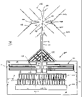
Figure 9 illustrates a switch package which includes a MEMS optical
switch in accordance to a further embodiment of the invention. The example
package 900 includes a housing 910 containing a 2x2 optical switch 920. The
switch 920 may, for example, be similar to the switch illustrated in Figures 1
and 2
above. Four optical fibers 930 extend from the switch 920 and outward from the
housing 910. The fibers 930 may, for example, interconnect the switch 930 with
other network components. While not shown, the fibers 930 typically run in
channels formed in a substrate body. Conductive leads 940 extend from the
combs
of the switch 930, typically to a power supply. It is noted that the package
is
provided by way of example and not of limitation. Many types of switch
packages
fall within the scope of the invention. For example, switch packages may be
provided which include external control circuitry (i.e., outside of the
housing) or
internal control circuitry (e.g., within the housing and, in some cases, on
the same
substrate as the switch). Moreover, while the exemplary package depicts a 2x2
switch, the invention is not so limited. Many different types of switch
packages,
such as 4x4, 8x8, 16x16 matrix switches, for example, may be formed by, for
example, cascading switches. Also, 1xN switches may be implemented with the
optical switches noted above.
As noted above, the present invention is applicable to the fabrication
of a number of different optical switches. Accordingly, the present invention
should
not be considered limited to the particular examples described above, but
rather
should be understood to cover all aspects of the invention as fairly set out
in the
attached claims. Various modifications, equivalent processes, as well as
numerous
structures to which the present invention may be applicable will be readily
apparent
to those of skill in the art to which the present invention is directed upon
review of
the present specification. The claims are intended to cover such modifications
and
devices.
12