Note: Descriptions are shown in the official language in which they were submitted.
CA 02379295 2002-03-27
OPTICAL DEMUL~'IPLEX1NG SYSTILM AN11 Mk:'fklUtt
This application relates tv an optical demulliplexinh systcur aii~l iuctliod
such as may be
amployed in the systom and method described in YJS prvvisi~onnl application
relating to a high performance optical m~tltiple~,ex and demultiplexer being
~xled on the same
day ns the present application by David,Boertjes and Kizn Roberts, to be
assigned to Nortel
Networks, under the Nortel Networks reference of 1358'780.
1.0
~IeI~ of llre Iuve~ri.iuxr
The invczition relates to an vptacal dcmultiplexing system and method, and
pa~rticula~rly to a
system and method for splitting an o;ptieal signal carwying a number of
informaticm rhanne:IS
at different frequencies-
Optical communicatiuus systci,us iiicreasW g1y use wavelength division
rnultiplexiag (WDM)
cc, which a number of distinct optical signals are transmitted at different
wavelengths,
generally down an optical fiber. )or example, optical eomnraunication in the
so-i:aLlPri "('."
band may allow the transmission of 4(.l rhannPic, nr frequencies, at regulaz'
Intervals, each
carrixig lOGb/s of data. ( Me nrt~cal signal can be transmitted at each
frequency down a slztgle
optical fiber. Ocher bands and/or other numbera~ of (:h~lIlIlCl~ lAldy ~:J~
used, for cxanaplc, 56
channels in the "L" band, each cari;yiu.k laCivls.
A key component in WDM systems is a demultiglexer for splitting apazt optscal
signals at a
plurality of wavelengths canto the individual channels at individual
rxravPlengths_ This may be
done using a splitter and a nuzx~.her rnt~ ctitferer~t filters tuned to the
iudi'vidual ftequencie5, by
components that rlemaltiplex the light directly, or a combination of these
appruacliCS.
One appzoach to Jihcrii~; acid deiuultiplcaing Xs to use an arrayed waveguide
grating (h.WG),
also hnowa as a phased-array device. The operation and design of A'WCfs is
described, for
CA 02379295 2002-03-27
example, in "PH,A,S11R Based WDM-Devices: Principles, Design and
Applications", Meint
K. Smit, IEEE Journal of Selected Topics in Qua~otuz~n klectronics, Vol. a,
No. 2., June lg9ti.
Figuz~~.s .l tn 3 illmtra.te an AWC device. Figure 1 shows a top view of the
AWG, FigurC 2 d
side sectiop through a waveguide of the AWG and Figure 3 is a Wailr.~l tcrp
view of pact of
the AWG ilcvice. A pltuality of optical waveguides 3 arc defined orz a
substrate 1 in a known
way. rot cycample, to define the wvaveguides a buffer layer 5 may bs deposited
on the
substrate, a core 7 deposited along part of the buffer layer to define the
wa~reguide 3 and a
cladding layer 9 provided to cover the core and buffer layers. The: refractive
indic-:es of the
1o buffer 5, care 7 and claddiuag ~l la~r~rc a.re selected so that light is
guided alone the waveguide
inn thp rPginn of the core.
ThC arrayed waveguidc device includes an array 11 of wavcguides 3 arranged
side by side on
the substrate acid extending between an input star coupler 13 and as output
star coupler 15.
The input and output star eouglers 13,15 are defined by a wide core regiaa in
which light ran
travel freely in the two-dime~usi~onal place of the substrate. 'I'hia region
is lmown as the free
rxoragatinn region. Input 1'7 and output 19 optical waveguides are proviQrci
lu frxd i~uWut
light into the array I 1 of waveguidcs~ arid to output light lrurn tLc ~,uxay
respectively. Theto
may be a plurallry of input wavG~ui~s 17 or output wavcguides 19.
ao
As an example Figure 3 illustrates the output star coupler of a system ~uvith
a sit~.gle i~nrnr
waveguide and a plurality of output wav~~yiclec. The ends 21 of the array of
waveguides 11
are usually oa a geozn.Ptrir, circle 2:i of radius r whose centre is at the
centre 25 of stn iruaxc
plane L7_ The output waveguides 19 are arranged on Ilia image ulaaae, which
also constitutes
a Circle. Note that the centres of Lhe circlCS am rout coincident, and rxzay
cot have equal radii.
The lcr~gths of the iadividuol waveguides 3 of the array 11 differ (see Figure
1) and the shapes
of the star couplers 13, 15 are ehose~n so that light input to t.bp inrnt
opt9cal waveguide 17
passes through the away 11 of vv~vngmrirs and creates a diffractioxl pattern
on the uutput
waveguide or waveguides, soc:h that light of~ a predetermined cenCtal
wavelength cr~~s a
central interference peak at the eentrE; ZS of the irna.~c NlauC. Light with
~z~equeacics slightly
k~igher or lower than the predct~crvr~.ue,d central frequency is imaged with a
eeatra~l iuntarferenee
peak slightly above or below the eenta~e of the image plane.
CA 02379295 2002-03-27
3
Irr order to achieve this recall the optical path leagth difference between
adjacsat waveguides
of the array is chosen so that it is an integral multiple of the central
wavelength. Accordingly,
light at the central wavelength whicla~ e~ntess the array of waveguides in
phase will Etlso leave
in phase and thus will create tho cetmral diffraction spot at the caatre of
the image plane.
Light with a slightly different frequency will arrive at the output star
coupler with sliXht phabe
differences across the array, which will cause the li,glat to be irnagcd to a
spot on the iumagc
plane a little a~wray ;Froxr~ the central spot.
Accordingly, the plurality of output Lvaveguidss arranged ca the output plane
receive light of
slightly rtifxrrrnt fre~cloPnoiea. Ndually spaced nutnut wavegtndes
eorre,Spand to equally
spaced frequencies, ac least to a first order of approximation.
Figw~e 3 shows tlic cffCCt of one yr more output warcguidas connected to the
output star
coupler 1S. It is alternatively or additionally possible to arrunga a
plurality of input
wavesuides ca the input stsir coupler vrith the same effect.
An Awt~~ hfla a. numher of properties. one important property is that the
distance of the
image spot along the image plane .as a fwnccion of wavelength is substantially
linear In
wavelength, for wtwClcnglLs at~uud flues ~GUual rivavaleugth. Accordingly, it
is possibly to
2o separate a number of signals wins regular channel separations by
pooxtiotting output
wavoguides at substantially regular intervals along the output place.
A second important property is that the A Wt t hoe a repeat. frequency. In
other words, the
interference properties as a funetian of frequency repeat with a period in the
frequency
~a domain. This period is known as ~ha IrCC spCCu'dl ~au~kG (1SR). The fine
spectral raiigc is a
function of the diaca in optical length between adjacont wavoguides; a large
optical
length difference results in a small 1=SIE~ and vice versa.
Although an AWG ran catty out demultiplexi~ng, i.t is not grnPmlly rractical
tc~ demultiplex a
30 large numlxr of rhannpls acing a cmgle AW'Ci_ For example, it can be
impracticable to
demultiplex each df the 40 channels in the C-band ubing a. sinklC A'9VG, fur
futu masuus.
pirsdy, the C-band covers avruc 4 000 G~ sr~ the AWG would need an rsR o~ at
least this
much. This would result in szz~all path length differences botw~en each
wavesuide of the
axxay of the AWG and hence a physically larse AWG device_ Secondly, it would
be
CA 02379295 2002-03-27
4
necessary to provide 40 output waveguides, which would also lead to a large
device. Thirdly,
the . accumulated cross-talJc into one; channel from the other thirty-tine
channels may be
excessive. Finally, in some applicatianc it is desired to process a group of
channels, e.g. far
e3isprrrasiun compensation, so a mulu-stage process might be preferred..
s
However, an nltarnativc systom with separate AWGa in cash frcquancy range
~rwould grcady
increase the parts count of an optical system and would hi~lcewise be
inconvex~ie~ut gad difFcult
to manufacture.
a o Accordingly, there is a need for an improved optical demultiplexer capable
of accurately
dividing an optical signal having a mudemte ur large number of uptical
channels inW
individual clia,uuels.
Fuztbencnox~, in sos~ne cases there is a need to apply some processing on
optical signals in
15 broad fxequez~cy bands as well as to divide the optical signal into narrow
freduency bands or
in~lirrichlstl channesl~.
Fuzther, tk~e mazlu;~ac;turing CUSIy or optical cornpunCnls eau 'tic
wusitlrravla and al wuultl be
beneficial to reduce these coats.
Sumauu~of Invention
In a. tirct aspect of the mventian there is pravided an optical system,
comprising: an optical
sputter for splitting an input optic~ti siarnal betwc~n optical outpms; and a
plurality of
deutuldplexers of like design, each demulliplexr~ hdvin~ a Nluralicy of iruNut
guides Durd a
23 ~lmali,ly of output guides, eacli input ~~uidc liaving a pncdetexxnined
fxequcncy range for which
optical signtals input into the input guide are divided between the plurality
of output ; aides
aeeordiab to frequency; wherein the optical outputs of the optical splatter
are connected to
respective demultiplexexs thro~.igh input guides having a rlurality or'
di.fke~ent rreciPter~rnineri
1'fP.1111Pnfy ranges.
~y providing a plurality of inputs fur lha accuullaNlr~xcrs it Is passable for
cacti dcmuldplexcr
to tlcniultiplea a subset of the fi~qu~cy band of the signal input to the
splatter, without having
to cope with tbie whole band. This; avoids any di,~culties in providing a
demultiplexer
capable of demultiplexiag a whole band. For example, in a systezx~
demultipiexyng 4U
CA 02379295 2002-03-27
S
channels in the C band, it is very difficult to design a single demultiplexer
capable o~ dividing
the 44 channels between 40 outputs evenly at~d with a suitably low insertion
loss.
lVtoreover, by using a plurality of dernultiplexers ~f like design, the
arrangement riecc~mec
s simple to manufacture. ~t is only necessary to connect a number of like
components to the
outputs of the splitter; there is no need to stock a variety of diffczmat
parts or to fittae tune the
dcmultiplcxcrs once in place. All that is required is to connect the correct
input.
The demultiplexers may be arrayed waveguide gratings with a plurality o~ imput
vvaveguxdes_
1o Arrayed wsuagaidc gratings with lszgr.. z~unr~.bers of o»tpnts tPnri t~
haves ~iittere~nt lnssPc
depending on the location of the output wavegulde. These differences can be
minimised by
having a reduced number of output w~3v~sguides and using a nuiut~r crf input
wa.vc~ui~s.
The predetermined frequency ranges of the input guides may span a
prcdatermincd input light
is frequency ranse without overlapping, so that the i~aput lxglat ~zequency
range can be split into
narrow frequency razages, which may <:orrespond to individual ehanaeZs.
The optical splitter may iu~elude filtering fttnetionality, for example at
least one coarse filter,
for dividing light info ptctlclcttuiutd vtua~l fcn~uctrcy' ranges output an
respective optical
20 outputs which in turn arc connected to input guides having corresponding
predetermined
frcquaney ranges. Xn dais way, cross talk between channels can be reduced. Any
light that is
output oaa tlae wrong output of the optical sputter, bec~u~ My im~rt's~aicms m
the coarse filter,
will be passed to a de~zz~.~a,ItirIexPr nphnal mrut that. cine~ not correspond
to its frequency, and
so the demultiplexer will not pass the light.
According to a second aspect of the invention there is provided an optical
ayatom for optical
processing of are optical eignnl divided into a plur'ty o~ predetermined
groups of chatuuels,
comprising: a plurality of optical outputs, each optical output outputting
signals is a
respective ~cequency range that corresponds to fi pxrrrlptArmined grnup of
channels: a plurality
30 of detnultiplexezs ox .like dt~cign, esch demultiplexer having 8 plurality
of iilput guides aDd a
plurality of output guides, each input guide having a predelerminGCl
tzr,~ucucy xai4ge fm wlucla
optical signals input into the input xuiJc a~wl,ivi~led between the plurality
of output guides
according to frequency; whcxein the optical outputs are connected to
respective
dcmultiplcxars, each optical output connected to the respective demultiplexer
through an
CA 02379295 2002-03-27
6
input guide having a predeteed ~x~equ~ency range corresponding to the
frequency of the
respective frequency range of the optical output.
The use of demultiplexers of like desi~ neatly simplifies the manufacture of
the device.
Thc~ is nu need lu alcnk a iiuiutrar u1 diIrCrCnt lypcs cun~spcrntiin~ W
tliffCiuiit frGducnuy
ranges. By like design is meant designs 'that arc largciy identical or
equivalent. The
dcnaultiplcxcrs may be of substaati~llvy identical design.
The demultiplexers may have cyclic properties that repeat in frequency wxtb a
period o~ the
free cpeetral range. l~n particular, the demultipiexers may be arrayed
viraveguide gratings.
A coarse frequency splitlan can Uc~ usaa fur vlivivl.iug au iwuuC optical
signal ilito the
predetermined garoups of channels.
x5 Separate dispersion compensation may be pravided for each of the
predetermined groups of
channels. In this w:~y, the dicpercinn c;nmra~nca.rian c:an he separately
aptimised for each
frequency range.
Xt is ~su NussiLle to provide separate gain control for the different channels
or gxoups of
20 channels.
Switches may be provided nn the inrntc of the demultiplexert for switching the
outputs of Lhe
optira.l Pmr,~ccing cP.ctmn intn the corresponding inputs, In this way the
switches can be
configured in a separate operation to manufacture, which simpliras
umufa~:u.uC.
The demultiplcxcrs may dwrnultiplo~c signals is frequency bands cvzrespondina
to each input
and reject sigrruls in adjacent frequency bands. Tn other words, signals in a
frequency band
adjacent to the frequency band corre:aponding to ate input are not
distritnit~i into any nt the:
outputs of the demultipiexsr.~. ' I'hys cstn reduce emss-talk.
The demultiplexers may be AWGS.
The A'W'Gs may be arranged to demultiplex the sigials of broad frequency range
to which
they arc u~ttached by realising that xhe: AWGs have properties that repeat ran
frequency with a
CA 02379295 2002-03-27
7
period of the free spectral range. ~'hus, for each input a differexlt group of
frequencies of
predetermined width within each free spectral range is demultiplexed and at
least one other
g~mup of tieque~ncies of prtuir,.rex~mine~i rxridrh is mjex:r~.zi_ '.i'ht
inputs of the AWI~~ cxmnfxaprt
to the outputs of the coarse filter cam rhea be selected to be cyclic with
increasing frequency
of the rewpecaive broad frequency rank whcrGin tlic cyclC rcpGals with a
mpc~tl fz~urtuy
substantially equal to the free speotr~al range such that each AWC
demultiplcxcs the signal
corresponding to the broad frequency rnngc of the output of the coarse filter
to which it is
attached.
l0 tsar cimrlicity, the AWt~ may have two configurations and the AoV'tas
comlectied to the
outputs of the coarse filter in ascending froquency order zriay be wn~gured
altcrnatGly in esu:h
of the two wn8gura~lon5_ However, ltris is nut csaGUtial au~l 1~ AWCfi may
have x laugec
number of configurations. por oxarnzple, if the AWG has three configurations
the cyclical
configurations in asccnditzg frcqucacy order may be first, second, third,
fist, second, third,
first ... etc.
~I'hc pmvision of a number of inputs wing effectively a number of
configurations of the
filters of common design brings advantages over the provision of only d single
ccmGgur~sliun.
Cur~idcr fitbl ra wuupa~atfve example of an A'~V'l'~ with a single
coafiguratian as the
dc~ociultiplcxcr. Each broad frequency range might include ~1 channels spaced
100GpIz apart,
~n,d am AWG of ~IOOGHz free spectral range and four outputs might be provided
for each
broad frequeaxcy range output to spilt rk~e bread frndueney range into
individual channels.
This alTaDgcmeDt would have the Clisadvantage that it would ruGtur thin lliC
wa~se~ filter had to
l~ be very precise with sharp C~1#tC uu~-wffe. Iu Gou~.crcial devices, i~ the
first broad frequency
range corresponded to chatuaels 1 to 4 it is likely that some signal in
ehaaael 5 would also be
transznuttcd into the output for chanzaels 1 to ~I since real coarse >Flltera
will transmit sozzre.
signal. a little outside the passband. '.If only a single configuration of
AW(.i ~re:~ nccjd, then
aa,~r signal in channel S whxrlt vcrac transmitted into the AWG on the output
of the coarse filter
rnrcPsPnn~iing to channels I to 4 would be output froze the channel 1 optical
output of the
AWG.
rear example, is cmbodimonts of the pxesent invention there may be two.iaputs
on the like
AWGs, one input for deznultiplexing chaxuc~els 1 to 4, channels 9 to 12 etc,
and the other fox
CA 02379295 2002-03-27
R
channels 5 to 8, channels 13 to 16, etc. rrr this way, if some extraneous
channel 5 signal is
transmitted by the coarse filter into the output corresponding to channels 1
to 4 the t3lter of
common design will not pass that extraneous signal into any of the channel
outputs for
clraumcla 1 to 4. Silllihwly, any ctlaulicl 4 sigzlal flint dppeurs in the
output fur the sound
broad Frequency rangy corresponding to channels 5 to 8 will likewise be
rejected.
According to a third aspect of the invention there is provided as optical
system, having an
optical processor for processing an optical signal divided into a plurality of
predetermined
groups of channels output on respe~ctivc optical outputs, and a plurality of
demultiplexexs of
lu 111Ce deslg~n corunected to tkte optical outputs, each demultiplexer having
a plurallry of input
guides and a plurality of output guides, each iliput ~ui~lc lidviua a
pi~c~lrslrrnliuCd firqucnuy
range for wluch optical signals input iltto the input guide are dividcri
between the plurality of
output guides according to fraqucncy; wherein the optical outputs tire
connected to respoctivo
detnultiplexers, each opties~l output connected to the respective
demultiplexer through an
z5 input guide having a predetermined frequeaacy range c:nrrecponding tc~ thn
trpdtte:ncy of the
respective group of channels of the nptical ouput.
Z'hC UpLil:~tl prUGCSSUI In7ly bc; is cu~rae; GllCr. Tltu~, 1110 illVCitliUll
pl~uvil~cs', iii iit~ul(!AC~~ aapCCl,
art optical system comprising: a coarse optical filter for divid~img mn
optical signal into a
plurality of predetezz~aizted groups a:E channels and outputting the groups of
channels on
respective optical outputs; a plurality of demultiplex~s of like design, each
deantiltiplexer
having a rhirality of input guides and a plurality of output guides, each
input guide having a
predetermined frequency range for tvhich optical signals input Into the input
guide are divided
belwexn ltiC plurtality of output ruiaca ac:culvliug to ficulueiicy; whcreiu
the optical
25 outputs ato cozt~nectod to rospective demultiplcxcrs, each optical output
connected to the
respective d~zlattltxple~cer through as input Snide having a prodetermined
frequency range
correepondiug to the frequency of the mspectiwe ,group of channels of the
optical output.
In another aspect there is provided an optical demuluplexer comprising: a
coarse filter having
3U a plurality o;P outputs for dividing an, input optical slgrlal into a
plurality UT ~IGtiCtCILVlnctl
~~ivxcl ftnWamicy ranges of prcdcbcnuincd width and outputting oath
prcdctcrmincd. broad
frequency range on a respective output; a plurality of arrayed wavcguidc
gxatings conacctcd
to respective outputs of the coarse filter For demult:iplexing optical signals
irl the respective
broad frequency ranges into a plurality of narrour i~i~equeacy ranges;
wliPrPin the arrayed
CA 02379295 2002-03-27
9
waveguide gratings have properties that repeat in frequency with a period of
the free spectral
range; the arrayed wavegtude gratings have ;gust and second input waveguides,
signals input
into the different input waveguidss rejecting and demultiplexing alternating
frequency range
of tHa said prcclelrraiinc~d width, the ~t input waveguide rejecting the
frequency ranges
denu~uplex~l Ly tllC sr.~;uua iupul W~IYG~uItiC and 1116 srx:und input
waveguide rejecting the
froqucncy ranges dcmultiplcxcd by tlne first input waveguide; and the input
wavcguidvs of the
arrayed wuveguide gratings connECtcd to the outputs of the coarse ~~tcr
altcrnat~c with
increasing frequency of the respeetiv~~ broad frequency range to that each
arrayed ~uvaveguide
;rating d~emultiplax~es the signal corresponding to the broad frequency range
of the output of
the coarse filter to which it is attached.
The ua~ruw ficque~~r:y ta;tgcs bray vc cWual iu. sine a,ctd 1110 b~~uatl.
fr~ucucy r~utgc~ ttuty cac:h
be the same intagrtil multiple of the narrow frequency range. The narrow
froqucncy range
may correspond to a single channel. :fn this vcm~y, the demultipletter
according to the inwantiott
rrtay divide an input optical signal including a number of channels into the
individual
rhannPls,.
Sy u'in~ lwu-iupul tuuhiplc uulpul AWGs, a. grr;ally rv;ducxd nutnbcr of
swi~cles can be
provided compared to as arrangement in which switches arc provided on the
outputs of the
11.WG. Furthermore, by providing trwo inputs it is only necessary that the
outputs cover a
range of half of the FSR. This greatly reduces utreveuness in power
transmission through the
AW(T, ~inee near tn the ecigec nt~ the hand an AWCt exhihirc syntttcantly
mcrea.~ed Inns.
Ifitrther, this arrangement is colourless, 3.e. each AWG can fn fact be
identical and cope with
lttc whulG of lira PSR, by wrrGCll,y a~ljusliug I,hc switcla.
Ag ran altcmativo vcay of implementing this approach each AWG can be
oonfigured by
connecting only the desired input of the AWG to the corresponding output. This
eliminates
any insertion loss caused by the switch, by making the selection of frequexccy
rangy at the
time of manufacture.
3U
The aoxrsG fihex tttdy be impl~nlrd unity a ~Wlillrt~ a;xd a pau of filters,
for tacauzple
~iC~~:l~~~~ rll~~.
CA 02379295 2002-03-27
Any i'xlter mtay be used as the coarse demultiplexer. For e~aruple, a
pvhrising filter may be
empl oyett.
By providuig a two stags doauullitrlcxcr up4icdl pitxxs5iug axn bG carried uul
on the ~eoup of
5 channels output by the coarse filters. '1'he optical N~ui,-cssiu~ uwy tic
Jis;pGrsiun wiupcnsa,lion.
The iaventioa also relates to a node for an optical tel~ommunications system
iaoluding a
desnultiplexer Rs set output above.
1u The invention also relates w an optical te~lecor~amunieations system
including: a orancmiscion
nu~lc yruvivlity a Wl?M uylic:~.l si'nal; t~ receiving node for receiving the
WDM optical
signal; and an optical fiber connecting the transmission and receiving nodes;
wli~erciu the
rxeiving node includes an optical demultiplexer as sot out above.
In another aspect, the iavention relates to a method of demultiplexing as
optical signal,
ineludmgv Aivtding the c~ticai cigna,l mto a numhPr of hrnari t~rP.dueney
handc; snprlying pac:h
of the broad frequency bands to an AWG to split each of the broad frequency
bands into a
~luAalily u,f uiu.~uw fiGquturoy vmd5; w[m~,esi~t ~LG A.'~VCt~ n~c u1 cuuuuuu
dGSigu aW have uaac
of at lca9t tvvo conl3gurations, and ehc configuration of the AWG conaeeead to
ouch of the
z0 plurality of outputs of the coarse filter in ascen.diz~g frequency order is
cyclical.
fi a yet further a.~p~t, the invention relates to a method of maltufacturlng
an optical
demuldplexer, including: connecting alt AWG to each output of a coarse filter
for dividiag an
optical signal into a ntuizber of broad frcqucn4y bands, wherein the AWGs have
a number of
diffcrcat configuraeioxts; and configuring the AWG such that the configuration
of the AWG
cotmcotcd to each of the plurality of outputs of the coarse ~tltor iz~
asoending frequency ordmr
is cydiaal.
3u For a better understanding of the invention spacfflc embodimoncs will now
be drscxibGd,
put~ly by way ur ax,auylG, with ~cf~eucc to tl~ av:v:ouyauying drawings in
which:
Figuuv 1 sliows a known A~VG device;
Figure 1 illustrates the cross section through a waveguide used in the AWf3
device of Figure
1;
CA 02379295 2002-03-27
11
Figure 3 is a sehezaabic drawing of the output star coupler of the hWG of
Figure 1;
Figarc 4 is a schematic drawing of a first embodiment of the invention;
Figure 5 is a schematic of an AWCi u.~ed in the amhtxlimemr n:f Figure 4;
Fi~ut~c 6 is a acl~malic drawing of a fivrst coi~ctpataxive example:
3 riguic 7 is a sclieulaxic Jya~viuK of a sCC;uu~l cuznparative example;
Figure 8 illustrates the iaacrtion loase;~ of the devices of Tigure 4 to 7;
Figure 9 illustrates an optical netrvark; riccarding to the inveation; and
Figure 10 is a schematic drawing of a second embodiment of the invention.
1U l~lgtafled Deccriutinn
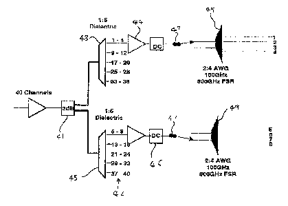
Figure 4 i5 a schematic drawing of a flr5t embodiment of the invention. A 40-
channel ~-hsnrt
iuNul 3iX~ld~ is pruvi~lC~l, in which a~lja<;cnt channels are separated by
100G~z.
The input signal is split by a 3dB sputter 41 into two, and passed to fast and
eooond ooarsc
15 filters 43, 45_ Ia this embodiaaent, the coarse filters are dielectric
alters. The first coarse filter
4'i has skive outputs 4Z, with passbands of channels 1 to 4, channels 9 to Z2,
channels 17 to 20,
channels 25 to 28 and channels 33 u~ 36 respectively. The second coarse filter
4~ likewme
has iive outputs d2, this time with passbands of channels 5 to 8. channels 13
to 1c5, channels
21 to 24, channels 29 to 32 and channels 37 to 4Ø
Each of floe teen outputs 42 is conztected to a lik~ a~yed waveguide grating
(AWG) ~19
thrnogh an ampii~k'ie~r 44, a riigPrrsion cornpPns~tor db and a two-position
opticRl switch 47_
:For clarity, only two of the AWGs are shown. The dispersion c~mpensator 4ti
and/or the
~atupli~ar 44 can be vzzullcd iI nw rcy,uind.
23
'The AWG is shown sohcau<tically iin Figuzo 5. It is a 2:4 AWG, i.e. with two
input
vvaveguidot~ 51, 53 forarAiuag inputs 48 a,nd 4 output waveguides 55, 57, 59,
61 forming outputs
:50_ ~'he input 63 and output 65 star couplers connect the input and output
waveguides to as
array 67 of waveguidee ti9 atrsng~d therebetween_
3U
~U L11C GXdILL~IG, lttC blrac;iur Uclwcxu lLa ityul wdvC~uidCS 51,53 al llic
ittpul. blot wuplCr 63 is
lfuuWilttcs llaat u~f lire uulNut wavcsguid.Gs 55, 5~, 59, G1 aL t~~a uulNW
star c:uuplr,,i 65_ '~'t,~is its
;shown schomc3tically by the dotted lines 52 in Figure 5 which correspond to
the omitted
~vaveguidas, not physically present waveguides_ Siztce the spacing of the
waveguides
CA 02379295 2002-03-27
'~ 2
cnrr~rrc~ndc (sea a ta.rst order of approximatioa) to the frequency spacing,
the frequency
spaCirig of the input waveguidee is assn four times shat of the outputs.
'Iz~. tb~c cxautple, thue spav::uy of lliG iityul wavcguidGS 51, 53 at the
input slat' coupler 63
S eorrcspoads to a 400GIIz sepsratioa ~uxd the spacing of tha ouc~ut
wavGKuidC' 55, 57, 59, 61
as the output star coupler 65 to a 100tsHz separation betweea wavoguidos. Tlto
AWG has an
804GHz FSR. In this vt~a~r, two input. waveguides ~8 at ~IOOGHz sps~cing cover
the >FSR, aid
nne nt'the, iagut wavegitides 51 caa be~. uSed for char~r~els 1 to 4, 9 to 12,
17 to 20, 25 to 28 and
33 to _ifi, and one t'nr rhannelc S tn H, 1.3 to lfi, 21 to 2.4, 29 to 32 aid
37 to 44_ Zt will be
to appz~eciated that a larger cumber of input wayeguldes zn~ay be used, if
reduired.
Althouglt only 4 wavcguidcs 69 in the array arc shown in riguuxe 5 the skilled
person will
appreciate that there will in practice normally be more, for example y5
wavoguidcs. Further,
the frequency separation o~ the output waveguides can be varied depending oa
the channel
i i xnacing n-mired.
'The dtsit;u ~,ul ~tuauurac;lw~ uI A'VV'Os is kuuwn ~tnci will nul be descs-
ibed further. The lateral
;3pacing between the wavcouidcs at the auray may be salc~aa<1 ~ua l~tc ~imtl
rcsulls. Gtuud
results have been calculated far devices with a small separation between
adjacent waveguides
20 in tho array, of order 6~u at the star eoupl~rs.
as
'Itefemng hACk to t~iyre: 4, at'ter man~~tac:W re: each of thp cwitc:hPS 47
c:nnnrrte~d to the airst
coarse filter 43 are srwitched to a fi~.-st position and each of the switches
4'7 connected to the
,~ecortd coarse ~,ltor 45 arc switched to a second position.
3~aoh of the AWGs is identical as aufacturcd. In other words, tltc A'~V'Cls
arc of common
design. Th~ AWGs sere configured by n~~ans of the switobes 47 oonnectsd to the
AWGs.
lNith the awitah in then tirct rnsitinn the AWITc rismultirlex nPtir:al
aignale at firpcjuerncy
3o corresponding to channels 1 to 4 and transmit the light into the four
output waveguides 55, 57,
iig, 61 respectively. Since the PSR as ~800C3~Hz, corresponding to 8 channels,
the effect of the
AWC3 rapaats array S cliaumals. Optivat signals In cluwnels 9-12 are likewise
divided between
t;he four outputs to separate the channels. nocordirigly, the light in
obeun~nels corresponding to
CA 02379295 2002-03-27
T3
thn tirst coarse filter 43 is sepd into the corresponding 20 outputs of the 5
AWCs3
connected to the flrct coarcc f~ltPr.
rf any light iti au i~icurt~cl, channel (e.g. cbatuael 5) should pass through
the 'First cnarSe filter
43 it will bo rejected by the AWCi siucc tw uutpul wrrcsputuls lu l6dt channel
with the switch
in the fast position. Tbus the atrunt,~ertacat of the proscnt iz~vcntion
reduces cross-talk.
.~.a~wise, with the switch irl the second position the AWGs derr~,uldplex
light of frequency
c~.orre~a~nding rn ahann.Pls S to $ and transmit the light unto ~our output
waveguides 55, 57, 59
X51 respectively. Since the FSR is 800GHz. corresponding to 8 channels, the
ettect of thp
,4'VSrG repeats every 8 clia~uuls acact li~,lit fiviu 4LG scc;und output of
the socond coarse filter 45
in channels 13 to 16 is lilnwisc ,split into four. AccordW gly, the light iu
cl~duu~cls
c;omesgaadiag to the second coarse :alter 4~ is soparated into the
corresponding ZO outputs of
the 5 AWGs connected to the second coarse filter ~I S.
1.5
Tri ihi8 w8y lriput light is &plit into 4C) sE:parate channelc tnr hirther
pmce.~cing.
7.."hc switches may be automatically c:uu~uarel aflcr cua,uur~u.:lwG of Iktc
cmnpleled devftce, by
software usod to eonfiguxe the dcmmltiplcxcr. In this way, the system can
readily be
r~nanufactured by unskilled personnel - it is simply necessary to connect one
like AWG to each
A~utput of a coarse filter. Thus, errors are avoided which ought result from
bad component
selecrion for arra~oigements where unskilled maaufaacuring personnel have to
select Ixtween
very similar components.
~!~ comparadvc example is illustratod in 1'iguro 6. ~ this approach, 1:8 AWGs
are uscrl
instead of the 2:~1 AWGs of the first e~nabodamor~t. ~ustead o~ a single
switch provided on tho
W puts a sepaurate switches 63 are provided on the outputs of each AWG to
cannect the outputs
corresponding to channels 1 to 4 n!- ~IVI/fT.c cnnnP.crPri to the tirst coarse
tiltecr 43 and the
outputs cort'esponding to channels 5 to 8 of AWGs connected to the second
coarse filter 45.
A. ~uzthcr co~miparativc example is illustlatcd iii Figut~c ?. Iu this
appu:oach, the swiahts aro
clipainatcd and two separate versions of AWG era used. A first version 71 is
used for AWGs
connected to the first coarse filter 43 sad a second version ?3 is used for
AWGs connected to
the second coarse titer 45_
CA 02379295 2002-03-27
14
In this arrangement, the rtiffe~mx~t versions of the AWC3s are utanufaatured
to substantially the
same design, with minor variation to provide the two separate
ectnfiguratictnF, nne whir..h
dcmultiploxcs clLauiwcls 1 to 4, 9 lu 12, 17 to Z0, 23 to 28 and 33 to 36 and
re,~ects Channels
to 8, 13 to 1 G, 21 to 24, 29 to 32 aunt 37 to 40, anti one the other way
around. This
axrangement removes the nocd to cantigurc the AWCs, at the cost of ono cxaa
component fur
'the parts bin.
A enmnaricnn nt theses appz~a~ches is shown in Figure 8, which shows the
insertion loss for
to Three embodiments. Figure 8a shows the results fnr the emhnriimrnt, Htgttre
xh for the first
v,Ot11j~31aLivG CX.~L~1C Ur ~l~ui'C 6 anQ Figure 8c for the second comparative
example of Figure
'7. The second comparative cxatnplc (.Figure 8a) sliows a luw ~utQ xGlalivaly
unifurm insertion
loss of only 2 dB. However, thi; embodiment uses two diffarcn,t AWGs. The
first
c:omparadve exatx~ple provides a less uniform insertion loss (,Figure 8b). The
larger numbor of
t 5 cmtpnt guides substantially fills the F'SR aid results in a less uniform
distribution of light
2~cross the output waveguides. 'l'ht:~ re:cWts in tnuvPr intPnsiries of light
being rsceived at the
outermost waveguides of the eight, leading to increased insertion losses for
these outer guides.
7:'he systom of the first embodixncnt ()~igtuc 8aj gives a good result, in
combination writh the
use of only a single type o~ AWG for nzanufaaturing convenience. A uniform
insertion la~.,s is
seen, although the loss is about 0.25dB higher than in the second comparative
example. 'f'his
increased insertion loss is due Co the off centre input wavegutdee mtc~ the
input star ennpler, a
less efficient position than the central input waveguide used in the
cotxtpararave examples.
zs 'Thus, by pmwiding a plurality of iztput guides the A'VVC~ only has to
detnultiplcx signals from
a pant of the FSIZ with each iutput guide. Thi3 increases the uniformity of
the output to a, lavcl
e~~mparable to that of the arrargenaent of Figure 7 without the corresponding
disadvt;ntabe of
nPx~ling tn stoc:Jr mnltip.le tarts.
30 lZ.eferring to Figure 9, as optical demultiplexer according to the
invention may be
ir.icurpolated into a nods of au optical uatwurk 91.
The optical network includes a transmassitor~ node 43 providing a WDM optical
signal, and a
receiving mode HS >:or receiving the WuM optical signal.. Jhigure N
illustrates two transnaisslOn
CA 02379295 2002-03-27
1.5
nodes y; and twn rp.~.Hiving nodes 95, though it is of course possible cc have
many axoxe. An
optical fiber link 97 Connects the transmissicm anti rec:Piviz~.g nodes.
5witahes !~y aannect
u~ausurisuun nudes 93 to receiving nodes 95.
s 'The rocciving node 95 includes an optical dcnnultiplcacr 9G for
dmuultiWlcxi~ux the WDM
signal as deacx~tbed above.
~4lthnugh the nntles are. lahelled transzxuission nodes 93 and reoelvixig
nodes 95, the spilled
person will appreciate that nodes may he ahlp tn timcti.c~n as both
transmission 93 and
to m~civing 95 nodes.
l'1 further ombodimont of an optical systa~on according to the invontion is
illustrated in Fietuc
1Ø A splitter 101 splits n cl~axmels between a plurality of outputs 42. The
sputter may
also incorporate some filtering so that each output carries a corresponding
group of channels
F,aeh group of channels then passes through a respective optical procector
4ei. 'f'he optical
l;~cocessors iu$y carry out any ~cyui~rvl. fua~clxVii, far cx~nple disprrsivn
wmpensation andlor
gain control.
T'he outputs of the optical processors 46 are then fed through switches 47 to
respective
dernultinle~xerc or fW es,alters 4y. ,i~ac:h o~ tk~e~se demultiplexexs 49 has
a plurality of inputs 48,
and the switches select the inputs 41i. Depending on which lzrput 48 of the
demultiplexer is
sclactr~l lry Ltic swilv;li 47, a rliffrrcttl licduency~ band is demuldplexed
and split between the
outputs 50. The switches are controlled so that the domultiplcxers dcmultiplex
the frcqucaicy
of the corresponding group of cba~cls passed through the optical processor.
Jzi this example, the demultiplexars are not necessarily cyclic and do nvt
necessarily repeat in
frequency. Accordingly, they may b~e implemented in a wider variety of
technnlngiec,
including arrayed wave~uide gratings, dielectric filters, Fabry Perot ~ltera
and i~ee space
~luf.~r-a,c:Lion ~ra,ling tlevic:e~t, for rxarupla.
By not requiring the t3ac Filters 49 to operate aver rho wrhalc frcgucncy
range of operation far
efich input the transmission loss and other properties can be made more
uniform.
CA 02379295 2002-03-27
r.r .
The prevision. of switches 47 eases manufactuz~e of the device since each of
the fine filters ~1.9
can simply be attached to eorreqp~nncling switehrs wit~hrn~t hRVUZg to specify
or accurately
dclcrlnine the required frequency range at the acme of manufacture.
s The splitter 101 need not have a filtering function, l.c. it eau 1~c d
simple sputter.
:N'everthaless, the sputter may include some ooarac filtering. preferably, the
fine filr~crs rajcct
adjacent frequencies to those demultiplexed. Tn oombiam~ti~on with the
selection on tho~inputs
to the fine tnltn~rc, I:T(1RC ffil~C can br rr.~luc.~ since any stray signal
from adjacent chs~naels is
t~ejected. The rejection need not he total; any rpdnctir~n. in the
transmission of adjace~M filters
lo can reduce cross-talk.
'.Che cmbodixncnts described above are purel~r exemplary and the skilled
person will be aLIC W
s~rrive at many coodificatioas to the embodiments without departing from the
scope of tho
claims.
xt will be apparent to the skilled person that although the description intact
to trnq»emcy hanris
Clra vdud5 need ncl be Cxprcssed in I~nas of &eduency, but may also be
oxpressCd in terms of
vvavelength, ckraaaucl yr any athcr label to distinguish frcgucucy bands.
'~~u~rthermore, although the invention hs~s bees described with reference to a
system having X10
channels in the G-band the skilled person will readily realise that a similar
system could also
b~e used to dez~oultiplex a different nmont~er of channels, or a different
frequency band.
v1 a modification of the invention, onr or more of the filters arc replaced by
an albcrnativc
2s fiiltor typo. For exaz~aplc, an interleaving or polarisation filter may be
used as the coarse filter.
~'hese use polarisation manipulation techniques to produce an :interleaving
filter that
ektectively separates groups of channels at the output into two orthogonal
polarisations. In
other words a wavelength dmiSyon rnult~plexed (W l)M) R1~,'fISI w separated in
the filter intn
n~o optical signals at its output, that a~.~e polarised at right ailgXes to
each other. A polarising
30 b~edrn Spliller i>aay they be used tti Sep~ate the twU UrthUgcinal
pOlar3.Sed 5igna15.
Such a filbcr itself consists of a stack of bircfringcnt wavcplabcs that arc
carefully set at the
appropriate angle to each other. The input optical signal passes through each
waveplate in
horn, and the components of the signal zpsolveri sleep tk~: prin~xpal axes of
Path waveplate
CA 02379295 2002-03-27
17
nxrc~riP,~a~x differing delays. In tb~is way the temporal pulse response aad
the frequency
l!~sponse of the filter aan he hnitt nn. Thr filtPac zesponuse repents at a
i~requency iuatervs~l that
ilapcnds on the optical thickness of rhn waveplates.
'.Chc coarse filter is aot absolutely required and may be simply replaced >ay
a ~7~litter, living
the filteriag to be cs~ied out by tha demultiplcxara.
In the; ~le:errihe~l rmha~iizn~;nts, the derrmltiplexerc of like design are
configmred using switches
or doting manufacture. In modification of thF mventinn, other arrmaolus nnay
he used, for
to example by connecting optical iYbers to alternative inputs or outpurs,
depending on the
c.onfi~uratian requires.