Note: Descriptions are shown in the official language in which they were submitted.
1
'Description
Optical coupling device
The invention relates to an optical coupling device for
injecting light between two optical waveguide end
faces, the geometric position of one optical waveguide
end face, for example of an optical fibre, being
capable of being varied with respect to the other
optical waveguide end face, for example of a strip
conductor of an optical component, with the aid of a
variable-length element, which carries one of the two
optical waveguides via a holding device and is
connected to the structure containing the other optical
waveguide, or is fixed to said structure, by means of
at least one holding block.
An optical coupling device is disclosed, for example,
by WO 98/13718. Coupling devices of this type are used
in optical filters based on the phased-array principle
having an input coupling face which light enters at a
specific geometric position, the geometric position
influencing the output wavelength of the optical
filter. Optical filters based on the phased-array
principle are used in particular as multiplexers or
demultiplexers in optical wavelengths multiplex
operation (WDM), since they exhibit low insertion
attenuation and high crosstalk suppression.
German patent application DE 44 22 651.9 describes how
the centre wavelength of a phased-array filter can be
defined by the position of an input coupling optical
waveguide which leads the light into the optical
waveguide. In this way, the centre wavelength of the
optical filter can be adjusted exactly by means of the
geometric positioning of the input coupling optical
waveguide or the input coupling fibre.
CA 02379404 2002-O1-16
- 2 -
Optical coupling devices are also used in narrow-band
wavelength multiplexers (DWDM) for optical waveguide
transmission technology. These components make it
possible, on the transmitter side, to combine the
signals from lasers of various wavelengths with low
losses onto a single glass fibre or, respectively, on
the receiver side, to divide said signals to a
corresponding number of receivers in a wavelength-
selective manner.
The particular advantage of narrow-band wavelength
multiplexers as compared with conventional wavelength
multiplexers lies in their narrow-band nature. As a
result, such a small channel spacing is possible that,
at the minimum attenuation of the glass fibre, that is
to say in the wavelength range around 1550 nm, a large
number of transmission channels, for example 32
transmission channels, can be accommodated. A DWDM
comprises a chip, to which waveguide structures with
the necessary geometry are applied. On the receiver
side, the input of the chip is the fibre with the
multiplexer signal, which is also referred to as the
input coupling fibre. On the output coupling side, a
corresponding number of fibres are fitted, which lead
the individual signals on to the receiver.
In optical waveguide transmission technology with DWDM,
the problem is that the characteristics of the chip
change sharply with the operating temperature. A
temperature change leads to a change in the refractive
index relationships and also the geometric
relationships of the chips. As a result, wavelength
shifts occur, that is to say the branch of the channel
between DWDM and the lasers and, respectively, between
the transmitter side and the receiver side is shifted.
For this reason, the shift in the centre wavelengths
must be avoided.
CA 02379404 2002-O1-16
CA 02379404 2002-O1-16
- 3 -
In order to avoid the temperature effects described,
passive temperature compensation has already been
proposed. The temperature dependence of the centre
wavelength can be compensated for by the fact that the
input coupling fibre is shifted vertically with respect
to the DWDM chip as a function of the temperature. This
shift is carried out by means of a variable-length
component which, as compared with the carrier material
of the chip, has a higher thermal coefficient of
expansion, for example by means of a variable-length
element made of aluminium. Then, as was described at
the beginning, the optical fibre is fixed to the
variable-length element, so that the end faces of the
optical fibre and of the optical conductor chip are
shifted parallel to one another, which compensates for
the influence of the temperature on the centre
wavelength.
In the practical implementation of this coupling
device, the connecting points between the holding block
and the chip, on the one hand, and the holding block
and the variable-length element, on the other hand, are
designed using adhesive bonding technology. In this
case, the bonding point between the holding block and
the chip is cured after the input coupling fibre has
been positioned optically relative to the chip.
In the case of this technology, the problem arises that
the bonded connections are subject to temperature-
dependent changes. As a result of different bond gap
widths, inhomogeneities and gassing-out of the
adhesive, mechanical stresses arise in the gap. This is
particularly critical in the case of bonded connections
between materials with different coefficients of
thermal expansion, such as aluminium and glass or glass
ceramic. The consequence of the thermally inducted
stresses is that a temperature change not only affects
the desired movement of the end faces of the optical
CA 02379404 2002-O1-16
- 4 -
conductor elements in relation to each other, but also
movements perpendicular thereto, that is to say
perpendicular to the plane of the chip or away from the
chip. These movements are undesired, since they lead to
an increase in the attenuation at the input coupling
point. The undesired movements may be prevented, at
least partially, by means of fixing the free end of the
variable-length element, but the fixing has to be
configured in such a way that the desired temperature
dependent movement is permitted.
It has already been proposed to provide a displaceable
guide on the other holding block. However, this type of
fixing requires very close machining tolerances of the
components and a great deal of precision mechanical
effort. Nevertheless, problems arise as a result of
friction and play in the guide.
By contrast, the invention is based on the object of
providing an optical coupling device in which movements
of the end face of the optical fibre perpendicular to
this face are suppressed and, at the same time, the
desired movement of the end faces parallel to each
other is permitted. In particular, an optimal coupling
device is to be provided which is compatible with the
established manufacturing and adhesive bonding methods
and permits adjustment of the input coupling point
before adhesive bonding.
In order to achieve the object, the optical coupling
device mentioned at the beginning is characterized in
that the variable-length element is connected to a
variable-length compensating element, whose length
changes with the temperature by the same amount but in
the opposite sense as that of the variable-length
element, and in that the variable-length compensating
element is fixed to a second holding block.
- 5 -
The variable-length element, which can consist of
aluminium, for example, in this embodiment of the
invention is lengthened by a compensating element made
of a material with a negative coefficient of expansion,
so that the result overall is the same thermal
expansion as in the carrier material, for example
quartz glass. As a result, although the input coupling
fibre is shifted in the desired manner, that is to say
the end face of the input coupling fibre moves parallel
to the input coupling face of the chip, no relative
movement takes place between the fixing points of the
two holding blocks and the carrier material, that is to
say the chip, since the total length of the variable-
length element and variable-length compensating element
is always of the same size. Therefore, the stresses and
shifts described above are minimized.
A further advantageous refinement of the device
according to the invention is characterized in that the
length of the variable-length compensating element is
selected, taking its coefficient of expansion into
account, such that the length of the variable-length
compensating element changes by the same amount but in
the opposite sense as that of the variable-length
element. In other words, only the combination of the
influences of the length of the compensating element
and its coefficient of expansion matters, so that
accurate matching of the coefficient of expansion is
not necessary.
In order to achieve the object mentioned above, the
optical coupling mentioned at the beginning is
characters zed in that the holding block has a U-shaped
part made of a material with the same coefficient of
thermal expansion as the chip, in that a T-shaped part
made of a material with the same coefficient of thermal
expansion as the chip is provided, in that the
variable-length element with the positive coefficient
CA 02379404 2002-O1-16
- 6 -
~of thermal expansion is connected to the T-shaped part
at its foot and to the U-shaped part at its base, and
in that two variable-length elements with a positive
coefficient of thermal expansion are fixed to the legs
of the U-shaped part, which consist of the same
material as the variable-length element and have the
same length as the latter, and which, on one side, are
fixed to the legs of the U-shaped part and, on the
other side, to the underside of the crossbar of the T-
shaped part. This coupling device is fixed or
adhesively bonded to the chip with the aid of the U-
shaped part. By means of the identical thermal
expansions of the three columns formed by the variable-
length elements and the U-shaped and the T-shaped part,
permanent adhesive bonding of the individual parts is
made possible, without the connection points being
stressed as a result of temperature expansions.
Therefore, the input coupling fibre can advantageously
carry out the desired temperature-dependent movements.
As a result of the additional parts, the desired fixing
of the upper end of the variable-length element is
achieved, so that temperature-dependent and time-
dependent changes in the adhesive bonding point between
the U-shaped part and the variable-length elements can
have only a minimal effect. Only the U-shaped part is
connected or adhesively bonded to the chip, and all the
other parts can move freely and, therefore, are able to
shift in the event of fluctuating temperatures and
corresponding expansion of the variable-length elements
with a positive coefficient of thermal expansion.
A further advantageous refinement of the device
according to the invention is characterized in that the
variable-length elements consist of aluminium which,
because of its material characteristics, is preferred
for this purpose.
Finally, a further advantageous refinement of the
CA 02379404 2002-O1-16
-
device according to the invention is characterized in
that the material of the variable-length compensating
elements is a glass ceramic with a negative coefficient
of thermal expansion, preferably the material of the
chip. This achieves a minimum influence of temperature
changes between chip and holding block.
Exemplary embodiments of the invention will be
described by using the appended drawings, in which:
Fig. 1 shows a side view of a coupling device
according to a first exemplary embodiment of
the invention;
Fig. 2 shows a plan view of a second exemplary
embodiment of the coupling device according to
the invention with the viewing direction in
accordance with the arrow B in Figure 3; and
Fig. 3 shows a side view of the second exemplary
embodiment of the coupling device according to
the invention.
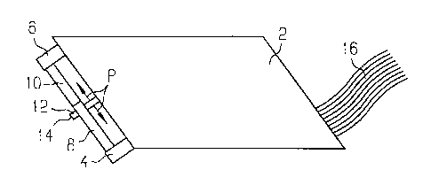
Figure 1 shows an optical waveguide chip 2 on which,
via two holding blocks 4, 6 (for example glass or glass
ceramic), a variable-length element 8 made of
aluminium, a variable-length compensating element 10
made of a material with a negative coefficient of
thermal expansion and a ferrule 12 are held, by means
of which an optical fibre 14 is held in an input
coupling position on the optical waveguide chip 2. The
ferrule 12 moves in the direction of the double arrow
P.
In this embodiment, in other words, the variable-length
element 8 is lengthened by means of a variable-length
compensating element 10, so that overall, the result is
the same thermal expansion as in the case of the
carrier material of the optical waveguide chip, namely
in the case of quartz glass. This means that, in the
CA 02379404 2002-O1-16
- g _
event of temperature changes, the input coupling fibre
is shifted in the desired way in order to compensate
for the centre wavelength, but that no relative
movement takes place between the fixing points of the
holding blocks 4, 6 and the optical waveguide chip 2.
Possible glass ceramic materials which have a negative
coefficient of thermal expansion can be obtained under
the names ROBAX~ or CERODUR~. Since the magnitudes of
the coefficients of expansion of these materials, as
compared with the coefficient of thermal expansion of
the variable-length element 8 made of aluminium, are
different, the length of the compensating element 10 is
matched in such a way that, overall, the result is
thermal expansion as in the case of the carrier
material, quartz glass.
On the side of the optical waveguide chip 2 located
opposite the input coupling side, the output coupling
fibres 16 are illustrated.
Figures 2 and 3 show a plan view and a side view,
respectively, of a second exemplary embodiment of the
coupling device according to the invention, Figure 2
having to be viewed in the viewing direction of the
arrow B of Figure 3. In this exemplary embodiment, a U-
shaped part 22 is provided as a holding block belonging
to the coupling device on an optical waveguide chip 20.
Fixed to the base 24 of the U-shaped part is the
variable-length element 26, which carries the ferrule
28 in which the fibre 30 is fixed. The other end of the
variable-length element 26 is fixed to the foot 30 of a
T-shaped part 32. Two further variable-length elements
34, 36 are fixed to the underside 38 of the crossbar 40
of the T-shaped element 32 and, on the other side, to
the ends of legs 40, 42 of the U-shaped part 22. In
this exemplary embodiment, the variable-length parts
26, 34, 36 are made of aluminium, which has a positive
CA 02379404 2002-O1-16
_ g _
coefficient of thermal expansion, and the T-shaped part
32 and the U-shaped part 33 are made of glass ceramic,
preferably of the same material as the optical
waveguide chip 20, the said material having the same
coefficient of thermal expansion as the optical
waveguide chip.
This construction results in three "columns", which in
each case consist half of aluminium and half of glass
material. As a result, all three "columns" in each case
exhibit the same overall temperature expansion.
Permanent adhesive bonding of the individual parts is
therefore possible, without the connecting points being
stressed as a result of temperature expansion. By means
of the additional parts, the desired fixing of the
upper end of the variable-length element 26 is
achieved, so that temperature-dependent and time-
dependent changes in the bonding point between the U-
shaped part 22 and the variable-length element 26 no
longer have any effect. Only the U-shaped parts 22 is
connected to the optical waveguide chip 20 or
adhesively bonded thereto. All the other parts of the
coupling device can move freely and can therefore shift
in the event of expansion of the variable-length
elements corresponding to fluctuating temperatures.
Output coupling fibres 46 are again shown on the output
coupling side of the optical waveguide chip 20.
CA 02379404 2002-O1-16