Note: Descriptions are shown in the official language in which they were submitted.
CA 02379483 2002-01-16
WO 01/08332 PCT/GBOO/02780
1
OPTICAL REGENERATOR FOR HIGH BIT-RATE OTDM SIGNALS
The present invention relates to an optical regenerator suitable for use with
optical time division multiplexed (OTDM) signals carried on an optical
network. The
signals may be, for example, optical packets or a circuit switched data
stream.
In order to use fully the bandwidth available on optical communications
networks, it is desirable to transmit time division multiplexed signals at a
very high bit
rate of tens or hundreds of Gbits per second. However, the very short duration
pulses making up such signals soon suffer degradation in shape, timing and
signal-to-
noise ratio resulting, for example, from noise in optical amplifiers,
dispersion in the
optical transmission medium and/or from the effects of processing at nodes
traversed
by the packet. Therefore, if the extent of the optical network is not to be
undesirably
limited, it is necessary to use an optical regenerator to restore the timing
and shape
of the pulse train making up the optical signals. Ideally, the regenerator
will function
as a"3R" regenerator, that is it will re-amplify, re-time and re-shape the
pulses.
Examples of suitable optical regenerators are described in Lucek J and Smith
K,
Optics Letters, 18, 1226-28 (1993), and in Phillips I D, Ellis A D, Thiele H
J, Manning
R J and Kelly A E, Electronics Letters, 34, 2340-2342 (1998). The use of such
techniques makes it possible to maintain the integrity of the optical data
signals as
they pass through a very large number of nodes. For example, Thiele H J, Ellis
A D
and Phillips I D, Electronics Letters, 35, 230-231 (1999) describe cascaded 40
Gbit/s
3R data regeneration in a recirculating loop. With a regenerator spacing of
100 km,
the error-free transmission distance in the loop is extended by an order of
magnitude,
from 200 km to greater than 2000 km. Regenerators made from semiconductor non-
linear optical devices, rather than fibre non-linear optical devices, are
preferred
because they are compact, stable, easily integrated, and operate at relatively
low
pulse energy.
Typically, an optical regenerator comprises an optical gate having a first
optical input that receives an optical clock signal at the data line rate, and
a second
optical input, the control input that receives the data signal that is to be
regenerated.
Typically the gate, which includes a non-linear optical element, changes to a
transmissive state when a binary digit '1' occurs in the optical control
signal that is
applied, and reverts to the original non-transmissive state after a certain
fixed time
: 22-05=2ti0~' - 00946158
CA 02379483 2002-01-16
2
6known as the gate window. The state of ithe gate.is,unchqnped= if a binary
digit '0'
occurs in the optical control signai, The state of the ntirt-liilear elc:meia-
thon
determines whether a given =puise in the optical clock train at lttc: inprrt
to the ctate is
passed on to the output from the gate. In this way, the bit pallr.rn in tlu:
input data
stream is imposed on the-opticai clock train and output to forrtii a rr
gerrer;ateci opticai
data stream. However, while experiments reported in Kelly A C et al, F-
ler:tranics
Letters, (in press, July 1999) have shown that semiconductor=ttaserl
aii=optic:al
%Y=~r~fi,ry r.regenerators can function at bit rates as.high as,80Gbitts it
has bec:rt fout7d that they
are unable to perform satisfactorily at stiii higher bit rates, -sirtaa
titPtti ir r general t ht,
bit period is very much iess than the recovery time of thc bptical gate, so
lhat the
regenerated signals contain patterning effects which lead to bit errors.
According to a first aspect of the present ittvention, tttiere is provided
tirr
optical regetterator including: (a) a data division stage arrartgNd to receive
an
incorning optical -data stream having a bit rate and to divide the incoming
optical ciata
stream into a piuraiity 'of further optical data streams~ cach having.a lower
t~it ratH
than the bit rate of the Incoming data stream; and, (b) d recteneratioii
slc+ctF, inr,ludirig
a plurality of optica) gate means each arranged to receive a respectivc: one
ot thc
further data streants at iti control input and to receive at anotttc:r input
an optir:al
clock stream at the frequency of the bit rate of the further data streanis or
a rrruitipie
thereof, wherein the outputs of the gate means are cor-rrur;tFCl in comrnuri
to mn
optical output (5) of the regenerator and arranged to provide o t=-it
irttr;rlFaved
r= egenerated optical data stream et the aeid output: ~ " ;. '
The present invention provides an all-optical generator that is able to
turtctivn
at far higher bit rates than existing designs. For example, us41f) crrrrer-t
tcctutuioctir;s,
an all-optical regenerator functioning at 160Gbitls can be constructed. ThE:
preserrt
inventors have realised that although the functioning of att optical rc:gcr-
erator is
limited by the recovery time of the optical gate, the impact ot tiiitt
recovc:ry tirne iy
different for a regular clock signal, as opposed to a signal cor7iprisinci ki
rartticrm data
sequence.' =.Accordingiy;= a gate that may: be=abie ;to function uftcctive;ly
as a ~ =~
. ,. , .. . +,
regenerator for data signais only up to 80Gbitls can nortettiNless function us
zi
demuitipiexer for-data signals at twice that bit rate. Tt=re regPncr=ator uf
t!-E; presrrnt
invention takes advantage of this difference to provide a systcrr- c:aprdblR
ot operatitiy
at far highcr bit rates. This is achieved by first dividittct ctuwiy the
higtter t,it r.ate data
;;r., .r:=~'~:~-:: a;. ~ = , . .
= = = = :;~~"= = ; . . ~ .. = . :~=. . . = ='
EmpfanssZeit 22-Mai= 11:25 AMENDEDSHEET
' 2G-~5-200
CA 02379483 2002-01-16
t. . } i
3
stream into a number of parallel data streams at a lower bit rate and t--c;r)
applying
these different divided data streams at the lower bit rate as cotitrol signals
to ct
number of gates, each of which is receiving a clock sigitai at the frequar7cy
of the
Y4:. ";5;nlower bit rate or a multiple thereof at its,input. Then,.when
the,:out'puts of thc
- . . , ...= , .
different gates are interleaved, the result is a regenerated data strcart) at
the higher
bit rate. '
Preferably the data division stage comprises a plurality of gate rnr;ans each
arranged to receive the data stream at a respective driving input cind a clock
strei:mi -
at the frequency af the lower bit rate at a respective control input arid
delay means
arranged to impose a different respective= deiay.on the' ciock siftnai at ttic
frequency
of the lower bit rate relative to the higher bit rate data sigriat for each of
the
respective gate means.
The alt-opticai regenerator may be arranged to function in a bit
syrrc:hrr,nous
network, in which case it may receive clock signals frorti local clock sources
1'hat are
synchroriised to a bit-level clock. In such a system, eaci- of the gate
rttcan;c rnay
comprise a single optical gate, for example using a TOAD (teraHertz optical
::1'~~f,p;=~1iu~~.i : . i ~ . e . :lirf' . . .
asymmetrical demultipiexer) structure.
Alternatively, the optical regenerator may be used in a network whicii
. = .
functions asynchronously at the bit-level. In this case, the optic:.jl
regenerator rnay
incorporate the regenerator structures described and claimed in ttic prc5e:nr
applicant's co-pending application PCT/GB99/01159. In tttis case, each of the
gate
means in the regeneration stage may comprise an array of opticaf gates, and
delay
means arranged to impose a different respective deiay~ in- the clock streafff
relative ro
the data stream at each of the array of optical gates, arid an optical
switc:l+
25. connected to the outputs of all of the array of optical gates, arid
;.irrangnci selectivcly
to output the optical data stream from one of the gates of the array.
AItnr',tiativciy,
as described in our co-pending application, a single gate means may tue iised
in
conjunction with means to shift the phase of the incoming packet to r-ratch
that of a
local free-running opticai- ciock source.
According to a second aspect of the present invention, thcrc is provided a.
A method of regenerating an optical data signal including:
~!z,:::EmpfanBsze.it 22.Mai . :11 :25 AMENDED SHEET
r ;:
0094P158
CA 02379483 2002-01-16
4
P ..
I1lrAtlly ol
. Ia) dividing ;ari incoming optical data signal; at,-a.bit rate into a 43
further data streams each having a lower bit rate than ttie bit rate of the
received
optical signal;
.(b) gating under the control of the plurality of further data streams a clock
signal at the frequency of the bit rate of the further signals or a niuttiplc
ttteryi>f; and
interleaving the optical signaia produced by step (b) thereby creating a re-
t's~-:a g1~.:p1,_generated odticai:signal,,at the bit.rate of the
receivedropticai data signal.
Systems embodying the present invention will now be described in further
detail by way of example only, with reference to the acconipatiyinci drawings
in
which:
Figure 1 is a schematic of an optical regenerator eryibodyitig the invention;
Figure 2 is a diagram showing an optical gate suitable for use in ths
regenerator in Figure 1;
. . ;-= ?i:4~~;;:~ . . ; = ;',- ~- :i . ,;,:.=~ ... s~=, :. .. . .
' Figure 3 is a diagram showing a gate array foruso in the: regeneratirug
stage of
an asynchronous optical regenerator embodying the invention.
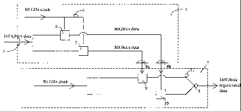
An optical regenerator comprises an optical data divisiot) stvgc 1ati(l an
optical regeneration stage 2. An optical time division rnuitipiexed tOTDMi
data
streartt at a high bit rate, in this example 1 fiOGbitls, is reccivcct at an
c,ptical iriput 3
of the data division stage 1. Divided data streams at a lower bit ratF;, in
this exarrtplc
14. : ' - i, ; '. . .. .. . . .
~' 80Gbit/s are passed from optical outputs 4a; 4b of the deta division
stagc;1 irrto the
optical regeneration 'stage 2. The data streams are used to gate ari
oF)tif:Fil clOck
signal at the frequency of the lower bit rate or a multiple thereof, iii this
exaniple 80
GHz, so as to produce at the optical output 5 of ttie regeneration stac;E: 7.
a
regenerated high bit-rate optical data stream.
In a regenerator for use with a synchronous data streatrn, tlic: data
divisiori and
w. regeneration stages requtre in total 2n opticai'gates vvftere n is the
ratio between the
., i
bit rate of the optical data stream and the lower bit rate of the divided data
strearns
input to the regerieration stage 2. In the present example, n --= 2 and there
are twu
optical gates in the division stage 1 and a further two optical gates in the
regeneration stage 2. As shown in Figure 1, each of the two'gates in t1tr:
division
stage 1 is connected In common to the optical input 3 and is drivorn by nce 1
fOGbit/s
optical puise stream. :An optical clock signal at the Iq,wer bit ratr: -of
ROC;I-iz is appiied
,. . . . . . . .
Empfanasieit 22.Mai . 11 ;25 AMENDED SHEET
: 22-Q5-20~11 pn~4F?58
CA 02379483 2002-01-16
. =
4G,
to each of the optical gates 6, 7. An optical delay 8 is included bet.weeri
the optical
feeds to the gates 6, 7." The magnitudeof the nptical~'delAy is said to be
equal to the
s~.r~, l..ti~y,j j ri~i . ~ ~ f.' ~ T. a ].,. . ~. : " =
= I'!; , , "t'.;~ = , , .. 1 . . ~ . , , ~]',!, ' ~. , , , _ ,
. . . , . . .
,7g:
. . . . ~7r I T
~ . . . = ~ . . ~ . = = = ~ =
= !..' ~:!~~~ ! ' ! '
a:7~ 'i~i~f=~1~;~~'.i~~,~-'~; :.I C . = . . ~ = . , . ... ,=': .'F~i.~=!1 = =
't' . . . , . . ~ . . . . , ~. . . , .. . . .
::'~'y~%5~'~tiV 'c~f,.14fj!f . . . . ' . . . . .. =~ , , t .
,=. . , . . . . . . .
Emvfan8szeit 22.Mai. 11:25 AMENDED SHEET
CA 02379483 2002-01-16
WO 01/08332 PCT/GBOO/02780
separation between successive bits in the optical data stream at the input 3.
As a
result, the two optical gates 6, 7 each pass every other bit of the input data
stream
with, for example, gate 6 passing the optical pulses in bit positions 0, 2, 4
... and the
other gate 7 passing the optical pulses in bit positions 1, 3, 5... The
resulting divided
5 data streams at the lower bit rate are passed to the optical outputs 4a, 4b
of the
data division stage 1. In the regeneration stage 2, a further pair of optical
gates 9,
are driven by the 80GHz optical clock signal. A respective one of the divided
data
signals is applied as a control signal to each of the gates 9, 10. An optical
delay 11
is included in the output from one of the gates 9, 10 and is arranged to
impose a
10 relative delay between the outputs of the gates 9, 10 that is complementary
to the
delay imposed in the data division stage 1. The outputs of the gates 9, 10 are
then
combined by an optical coupler 12. In this way, the two lower bit rate data
streams
are modulated onto the higher bit rate clock and interleaved to produce an
output
signal at 160Gbit/s that is regenerated in shape, amplitude and timing, that
is it has
undergone 3R regeneration.
Figure 2 shows one possible construction for an optical gate for use in the
circuit of Figure 1. In this case, the gate uses a TOAD configuration. A fibre
loop
mirror 21 includes a non-linear element 22 which may be, for example, an
optical
semiconductor amplifier. The non-linear element 22 is offset with respect to
the
centre of the loop mirror. The duration of the switching window is determined
by the
extent of the offset. A gating control signal is applied to the loop via an
optical
coupler 23.
Fibre loop mirrors in which the fibre itself acts as the non-linear element
are
described, for example, in Whittaker et al, Optical Letters, vol. 16, page
1840
(1991). The use of non-linearities in semiconductor optical amplifiers as an
ultrafast
gating device is described, for example, by Kang et al in the International
Journal of
High Speed Electronics and Systems, vol. 7, page 125 (1996). As an alternative
to
the use of a semiconductor optical amplifier in a loop configuration as shown
in
Figure 2, an optical gate may use a pair of amplifiers in a Mach-Zehnder
interferometer configuration. Another ultrafast optical gate is the ultrafast
non-linear
interferometer switch described by Hall and Rauschenbach (Paper BD5,
Proceedings
of Conference on Optical Fibre Communications (OFC '98) Optical Society of
America, February 1998). It is characteristic of all these devices, that they
suffer
CA 02379483 2002-01-16
WO 01/08332 PCT/GB00/02780
6
significant speed limitations as a result of the recovery time of the non-
linear element
when the gate is driven by an irregular data signal. However, they can
function at
considerably higher data rates when driven by a regular clock signal.
To generate the clock signals at and the frequency of the lower bit rate, a
clock recovery circuit may be used to derive a clock signal in synchronism
with the
incoming data bits and this clock signal may be used to synchronise a local
pulse
source running at 80GHz. For example, the clock recovery circuit may comprise
a
passive pulse replication network that replicates a marker pulse to produce a
regular
pulse pattern.
In an alternative embodiment, the optical regenerator is arranged to handle
incoming optical packets that are asynchronous at the bit-level. In this case,
each of
the single optical gates 9, 10 in the regenerative stage of Figure 1 is
replaced by an
array of gates. One such array is shown in Figure 3. The array comprises four
optical gates 31, 32, 33, 34. Each of the gates is driven by the 160Gbit/s
data
stream. Different relative delays of a fraction of a bit period are included
in the input
paths for the driving signals. This delay has a value of 0 for the input to
the first
optical gate 31 n/4 for the second optical gate 32, Tc/2 for the third optical
gate 33,
and 37r/4 for the final optical gate 34. The outputs from the four optical
gates are
passed to a 4:1 optical switch which selects the data stream from one of the
gates
to be passed to the respective optical output 4a, 4b. The appropriately
synchronised
output may be selected, for example, by tapping off a fraction of the output
from the
switch C and measuring, for example using a photo detector, the optical energy
in
the data signal each of the different gates is selected. When the phase error
between the clock signal and driving data signal is minimised, then the
corresponding
gate output will give a peak in the energy function. Electronic control logic
may be
used to generate an electronic control signal for the 4:1 switch. The lower
switching
rates of electronic control logic is not a limiting factor, since the
selection of an
optical output from the gate array only needs to be repeated at the packet
rate. In
such systems handling bit asynchronous optical packets, the optical clock
signals
may be derived from free-running optical pulse sources. A suitable source
comprises
an electronic microwave oscillator driving an electrically synchronised laser,
such as a
gain-switched laser or an actively mode-locked laser. Alternative, a
continuously
free-running optical pulse source such as a passively mode-locked laser may be
used.
CA 02379483 2002-01-16
WO 01/08332 PCT/GBOO/02780
7
In general, an asynchronous optical regenerator will require 5 n gates, where
n is the
ratio between the higher bit rate and the lower bit rate.
Figure 4 shows, by way of example, an optical network in which a node
includes a bit-asynchronous regenerator embodying the invention. Packets
arrive at
the node referenced B from a number of sources, each of which have
independent,
uncorrelated clocks. . By suitable adjustment of the transmitted power at the
source,
the power levels in any optical amplifiers used in the link, and also the
power levels
at any synchronous regenerators used in the link, the bits in the packets
arriving at
the input of a routing node may conveniently have an intensity at an
appropriately-
defined standard 'digital' level (e.g. of the correct intensity to perform
complete
switching in the optical gate or gates used in the bit-asynchronous packet
regenerator AR in the switching node). The inputs to the switching nodes will,
in
general, be bit-asynchronous. Each input to a routing node may pass through a
bit-
asynchronous packet regenerator AR, constructed as described above. As is
shown
schematically in Figure 4 a node, such as that referenced node B, may combine
an
add/drop function for local traffic as well as regenerating packets for onward
transmission.