Note: Descriptions are shown in the official language in which they were submitted.
CA 02379869 2007-04-03
VARIABLE OSCILLATOR
[0001] This invention relates to variable oscillators, in
particular oscillators whose frequericy of oscillation is
variable iin response to a frequency setting signal and which
can be trimmed by means of a separate trimming signal.
[0002] "'Figure 1 shows one form of variable oscillator. The
circuit ot figure 1 ineludes a resonant portion 1, which
produces an oscillating signal at 2, and an amplifying stage
3, which enhances the signal at 2 by sustaining the resonance
of the resonant portion and amplifying it to yield on
oscillator output signal at 4. The resonant portion comprises
a capacitance 5 and an inductance 6 connected in series.. =The
capacitance is a variable capacitance ("varicap") diode 7
whose capacitance varies in dependence on the voltage applied
at a control input 8. Thus the frequency of the oscillator
can be varied by means of that voltage, and the oscillator is
a voltage-controlled oscillator.
[0003] In many applications of oscillators such as the one
shown in figure 1 there is a need to arrange the oscillator
accurately so that a pre-defined range of frequencies can.then
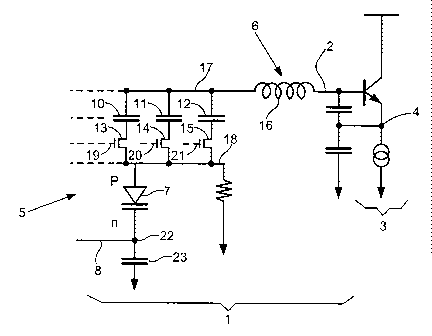
be.tuned over exactly using the varicap diode 7. For example,
in many communications applications the oscillator may be
1
CA 02379869 2007-04-03
required to operate at one of a number of pre-defined.
frequencies that correspond to the frequencies of av.ailabl.e
communication channels. In order for the communicat-ions
terminal that uses the oscillator to establish communication
with another terminal the frequencies used by the two
terminals must match each other precisely. In pro,duction
there is often significant variation between the values.of the
circuit components between individual oscillators. This is
especially significant.when.the oscillator is built on-chip.
(Typical variation in the values of on-chip components are:
30% for resistors, 10% for capacitors and 7% for.inductors;
the values also being strongly dependant on temperature).
Therefore, it is common for the oscillator to be trimmed after
production so that the pre-.determined channel frequencies can
then each be selected by applyin.g a corresponding channel-
setting voltage at the control input 8.
[0004] One way to perform the trimming operation is by using
the varicap diode 7 itself. A trimming offset voltage can be
applied to the control input 8 to ensure that when the
channel-setting voltages are also applied to the control input
8 the pre-determined channel frequencies are generated
.accurately. However, this approach requires the varicap
diodes to have sufficient throw (range) to be capable of
adjusting the resonant frequency not just over the.frequency
envelope of the available channels but also over an additional-
range to cope with the need for trimming the circuit. The
required total throw is typically around 30%. The effect of
this is that, compered to one of smaller throw, the varicap
diode is more sensitive to the voltage at the control input B.
2
CA 02379869 2007-04-03
As a result, in norznal, operation it is more difficult to
control the varicap diode accurately. Furthermore, the. wide
pull range implies tha.t.much of.the oscillati.on energy of the
circuit passes via the varicap dio.de 7, which typically have
much higher losses (i,e. lower Q) than fixed value capacitors.
High loss causes poor phase noise, which substantially
degrades the performance of radio, receivers, which are a
common application of variable oscillators. Another problem
is that if the.varicap:diode has a. large throw then the
variation, in voltage at the.control input 9 as a result of the
oscillation.can itself alt-er the. capacitance of the varicap
and therefore modulate the frequency of the circuit. In
addition, where the oscillator is_used with a phase-locked
loop (PLL) the wide range of.effective capacitance of the
varicap 7 means that the loop gain of the PLL is subject to
variation. This results in poor settling, which is not .
compatible with the rapid jumps-needed for frequency hopping
systems. Although this can be addressed by introducing an
adjustment for the loop time constant, this is an expensive
operation during manufacture.
[0005] Another approach is to use the circuit of figure 2.
In figure 2 like components are numbered as for figure 1. In
the circuit of figure 2 an additional mechanical trimmer 9 is
provided in the capacitative portion 5 of the oscillator.
This allows a varicap diode of smaller throw to be used.
However, the mechanical trimmer is bulky, relatively expensive
and requires an inconvenient step of mechanical adjustment
durin_g production. A-s an.alternative to a mechanical trimmer
the capacitan.ce 9 could be provided by a on-chip (monolithic)
3
CA 02379869 2007-04-03
capacitor that can be adjusted during production by laser
trimming. However, this approach is inconvenient because it
can only be done before the monolithic component is packaged,
and expensive because the laser trimming step has a low yield
and is incompatible with conventional integrated circuit (IC)
processes.
[0006] In another known arrangement the continuously
variable capacitance unit (e.g. represented by varicap 7 in
figure 1) are arranged in parallel with a finitely variable
capacitance arrangement which is capable of capacitance steps
just a little smaller than the sweep range of the 'finitely
variable capacitance. With this arrangement a first coarse
tuning operation can be carried out after manufacture using
the finitely variable capacitance arrangement to bring desired
capacitances within the sweep range of the continuously
variable capacitance. The setting of the finitely. variable
arrangement is then fixed. Then during use the continuously
variable capacitance can be adjusted to give precisel_y the
desired capacitance. However, the coarseness of the first
tuning operation means that the continuously variable
capacitance frequently. has to operate substantially outside
its optimum range.
[0007] There is a need for a variable frequency oscillator
that can be trimmed more easily and economically, without
significant deterioration in performance.
[000e3 According to one aspect of the present invention
there is provided a variable frequency oscillator comprising:
4
CA 02379869 2007-04-03
an oscillatory circuit for generating a periodic output
dependant on the capacitance between a first node and a second
node of the circuit, and having a capacitative element
connected between the first node and the second node; the
capacitative element comprising: a variable capacitance unit,
the capacitance of which is variable for varying the frequency
of the output; and a plurality of trimming capacitances each
being selectively connectable between the first node and the
second ndde in parallel with the variable capacitance unit to
trim the frequency of the output. In this aspect of the
invention a switch (preferably.an electrically sensitive
switch such as a transistor) is suitably connected in series
with each trimming capacitance between the first node and the
second node for selectively connecting the respective trimming
capacitance*between the first node and the second node in
response to a respective.switching signal.
[0009] According to a second aspect of the present invention
there is provided a variable frequency oscillator comprising:
an oscillatory circuit for generating a periodic output
dependant on the capacitance between a first node and a second
node of the circuit, and having a capacitative element
connected between the first node and the second node; the
capacitative element comprising: a variable capacitance unit,
the capacitance of which is variable for continuously varying
the frequency of the output over a frequency range; and a
plurality of trimming capacitances each being selectively
connectable in series with the capacitative element to trim
the frequency of the output in steps of less than half the
width of the said frequency range.
CA 02379869 2007-04-03
[0010] The trimming capacitances are preferable finite
capacitances.
[0011] The plurality of trimming capacitances preferably
provide a finitely variable capacitance unit. The trimmin.g
capacitances are suitably selectively connectable in parallel
with each other.
[0012] The oscillator may comprise control apparatus for
causing a set of the trimming capacitances to be conne.cted
between the first node and the second node. The oscillato.r
may also comprise a memory coupled to the control apparatus.
for storing information defining one or more sets of the :
trimming capacitances. The control apparatus and/or the
memory may also perform other functions in any device of which
the oscillator forms part. Each of the said one or more sets
may correspond to a respective operating frequency.of the
oscillator. The control apparatus may be capable of
retrieving the information defining one of the sets in
response to information defining an operating frequency being
supplied to the control apparatus. The control apparatus may:
be capable of retrieving from the memory information defining.
one of the sets and then causing that set of the trimming
capacitances to be connected between the first node and the
second node.
[0013] At least one of the trimming capacitances may have a
different capacitance value from another of tile trimming
capacitances. Preferably all of their values are different.
[0014] The trimming capacitances are preferably capable of
trimming the frequency of the output in steps of less than
half, and most preferably less than a tenth of the width of
6
CA 02379869 2007-04-03
the frequency range over_wh'ich the continuously-variable
capacitative element is by itself capable of providing
adjustment. The trimming capacitances preferably provide f.or
more than 10and most preferably:more than 40 or 50 finite
adjustmerit steps.
[0015] The capacitance of the variable capacitance unit may
be variable by:means of-the.voltage applied to an input of the
variable_capacitance.. There,may.be.feedback apparatus such as
a phase-locked loop connected between the output and the
variable capacitance.input_fdx..stabil.ising the oscillator.
The variable capacitance unit:is.preferably continuously
variable.
[0016] The oscillator,..or the oscillatory circuit, is
preferably formed.on a single _integrated circuit. .
[0017,] The present invention also provides a method for
operating a variable frequency.oscillator as described above,
the method comprising: retri_.eving from the memory information
def-ining a set of.the tri.mming.capacitances; connecting that
set of the trimming capacit.ances between the first node and
the second node; compariag the voltage at the variable
capacitance input with a first-p.'i~eset voltage range; and if
that voltage is outside.the f:irst preset voltage range
determining, based on the voltage at the variable capacitance
input, an adjusted set of the trimming capacitances and
storing in the memory information. defining that adjusted set
of the trimming capacitances. The said step of determining
may:be performed only if the voltage at the variable
capacitance input is inside-a second preset voltage range.. In
thestep of storing, the information defining the adjusted set
7
CA 02379869 2008-01-16
of the trimming capacitances may be stored so as to replace in the memory the
said information defining a set of the trimming capacitances.
[0018] The present invention will now be described by way of example,
with reference to the accompanying drawings in which:
Figures 1 and 2 show two forms of variable oscillator known from
the prior art.
[0019] Figures 3 and 5 show the circuit of a variable frequency oscillator
according to the invention; and
[0020] Figure 4 shows a control arrangement for the circuit of figure 3
and 5.
[0021] In Figures 3, 4 and 5 like components are numbered as for Figure
1.
[0022] Figure 3 shows a variable oscillator circuit for a radio terminal,
which can be implemented on a single integrated circuit. The variable
oscillator
circuit shown in figure 3 comprises a resonant section 1 and an amplification
stage 3. The resonant section includes a capacitative section indicated
generally
at 5 and 6 and an inductive section 7. In the circuit of figure 3 the
capacitative
sections include an array of switchable trimming capacitances 10, 11, 12 etc.
which can be selectively switched into the resonant, circuit by respective
transistors 13, 14, 15 etc. to allow the circuit to be trimmed digitally.
[0023] In more detail, the resonant section of figure 3 includes
an inductance 16 connected between node 17 and the
-8-
CA 02379869 2007-04-03
output node'2 of the resonant sect-ion. The capacitors 10-12
are connected in parallel between node 17 and node 18. In
series with each capacitor 10-12 is a respective switching
transistor 13-15. Each switching transistor is connected so
that when a suitable voltage is applied to its gate from the
corresponding switching input line 19-21 current can flow
between its source and drain so that the capacitor with which
it is connected in series is coupled between node 17 and node
18. A varicap diode 7 is connected between node 18 and node
22. Node 22 receives a voltage input from 8 to select the
operating frequency of the oscillator in use. Node 22 is
decoupled from ground at radio frequency by decoupling
capacitor 23.
[0024] After the circuit has been manufactured on-chip it
can be trimmed by switching one or more of the capacitors 10-
12 etc. fully into or out of the circuit between nodes 17 and
18 and thereby altering the effective capacitance of the whole
resonant section 1 of the oscillator.
[0025] The trimming of the circuit could be performed each
time the terminal is turned on, for example by comparing the
output of the circuit with a standard received frequency.
Alternatively, the trimming operation could be performed at
the manufacture*stage. Since each trimming capacitance is
switched fully into or out of the circuit the trimming is a
digital operation. The setting of the switching transistors
13-15 etc. can be represented as a binary number with one
digit corresponding to the switching input to each switching
transistor. The setting of the trimming capacitors can
therefore be stored digitally by memory of the radio terminal
9
CA 02379869 2007-04-03
during manufacture or use and reproduced exactly when required
by recalling the appropriate'setting from memory. More than
one setting could be stored (either at manufacture or during
use) for different applications, such as different operating
frequencies or temperatures.
[0026] Figure 4 shows one preferred arrangement for
controlling the oscillator 1, 3. The output of the oscillator
passes to a PLL 24 comprising a divider 25, a phase detector
26 and a loop filter 30. The difference in phase of the
divided signal and reference signal is fed back to the control
input 8 of the oscillator. The switching control inputs 19-
21 etc. of the oscillator are driven from an oscillator
control unit 27. 'The control unit is under the supervision of
a main processor 28 of the radio terminal. The control unit
27 monitors the voltage at control input 8. The control unit
27 adjusts the switching of the trimming capacitors with the
aim that the voltage at 8 is as close as possible to a preset
value. By performing this operation at each operating
frequency of the terminal, the control unit 27 keeps the loop
gain of the circuit relatively constant.
[0027] The control unit 27 could retrieve preferred settings
for the switching inputs 19-21 etc. at each operating
frequency from memory 29. To switch frequencies the control
unit could then apply the stored settings to the inputs 19-21
and leave the analogue PLL to settle any residual frequency
error. In this arrangement there could be no need for the
control unit to influence the voltage on input 8 directly, so
the oscillator control could be fully digital. The combined
setting of the inputs 19-21-etc. could be viewed as ,a multi-
CA 02379869 2007-04-03
bit binary trimming set signal from control unit 27.
[0.028] The table o.f trim code settings for the switching
inputs 19-21 could be stored in memory (e.g. as a table of
multi-bit binary numbers).by the control unit 27, during
start-up or as a background task, or during manufacture of the
terminal. One algorithm.for assembling the table during use
is as follows;
1. Apply to the switching inputs the digital code stored in.
the look-up table for an operating frequency.
2. Wait for the PLL to stabilise.
3. Digitise the voltage at the varicap input 8 by means of an
A-D converter in the control unit 27.
4. Compare-the digitised voltage with a first preset voltage
window. If the voltage is inside the first preset window then
keep the present digital code setting.
S. If the voltage at the varicap input is outside the first
preset window then compare the digitised voltage with a
second, wider preset window. If the voltage is inside the
second preset window then maintain the present digital code
settings for the current radio activity (e.g. for transmitting
or receiving a packet or burst of data) but adjust the code
stored for the present frequency so as to increment or
decrement (as appropriate) the trimming capacitance that is
switched in for the present operating frequency. The adjusted
11
CA 02379869 2007-04-03
code will then be employed the next time the present frequency
is chosen.
6. If the voltage at the varicap input is outside the second
window (in which case the unit is off-tune) abort the current
radio activity and enter a re-calibration mode.
[0029] This method could also be used during a built-in
self-test (BIST) operation in the terminal. The above method
could be cycled through for each operating frequency.. A self-
test feature of this type can yield significant cost savings
during production and is desirable for ensuring proper
operation during use.
[0030] Whilst the transceiver is enabled it preferably
continuously monitors and adjusts the digital code applied to
the transistor switches to keep the analogue variable
capacitance at or near its optimum capacitance value.
[00311 The array of capacitors may include any number of
capacitors from two upwards. The values of the trimming
capacitors could be the same or different. If the values of
the trimming capacitors am different then the same number of
trimming capacitors can be used ta allow trimming over a wider
range, saving an IC real estate. The trimming capacitors
could suitably provide 128 equal steps of total capacitance.
This could, for instance, be achieved by 128 capacitors of the
same value, or 7 capacitors of values scaled factors of two
apart.
[0032] In the re-calibration mode the control unit 27 could
12
CA 02379869 2007-04-03
repeatedly monitor the voltage at the varicap input an.d
increase or decrease the effective total trimming capacitance
by switching one or more trimming capacitors in or out as
appropriate until the varicap input voltage is within the
first or second window. If the steps in values of the
trimming capacitors are the same then a very simple trimming
algorithm can be used in the control unit 27 to adjust the
effective total trimming capacitance monotonically simply by
switching in more or fewer capacitors. If the value.s of the
capacitors are different then the trimming algorithm should
take this into account.
[0033] Step 5 of the algorithm set out above is especially
beneficial because it allows for gradual changes to counteract
drifts (due, for instance, to temperature fluctuations)
without the need for full re-calibration.
[0034] The trimming capacitors 10-12 are in parallel with
each other and in series.with the varicap diodes, as shown in
FIG. 3. The trimming capacitors could alternatively be in
series with each other and with the varicap diodes,'as shown
in figure S.
{ [0035] The finitely adjustable portion of the capacitative
section preferably allows around 50 or more finite capacitance
steps, with a step size substantially smaller than the range
of the varicap. This allow the varicap to be not just pulled
into range at a selected finite step, but to be arranged so
that a desired narrow part of its continuously variable range
will yield the desired capacitance. This provides better
controlof loop time constant and loop response compared to a
system in which at only one step setting can the varicap give
13
CA 02379869 2007-04-03
the desired overall capacitance. [0036] The range-of the continuously variable
capacitance.
(in this example the.varicap) preferably provides for
frequency adjustment over a very much smaller range:th-an-the.
total range of variation available from the capacitative
section including also the finitely variable capacitance
circuitry. This provides much better phase noise performance
than a system in which the continuously variable capacitance
accounts for a major proportion of the total adjustment ran-g.e.
The radio terminal-could be a radio trarlsmitter and/or
receiver. The terminal could operate according to any suitable scheme,
including TDMA (time division multiple
access) and FHSS (frequency hopped spread spectrum). The
oscillator could be used in other applications such as tone
generation. [0037} Numerous changes could be made to the circuits shown
in figures 3 and 4. For example, the output stage of the
oscillator could be varied as required. The varicap 7 co.uld
be replaced or supplemented by one or more other forms o.f
voltage, current or manually controlled capacitance, or only-
one variable capacitance section used, rather than the
symmetric example shown in figure 3.
[0038] The applicant draws attention to the fact that the
present invention may include any feature or combination.of
features disclosed herein either-implicitly or explicitly or.
any generalisation thereof, without limitation to the scope of
any of the present claims. In view of the foregoing
description it will be evident to a person skilled in the,art that various
modifications may be made within the s.cope of the
invention.
14